Article
Formation and characterization of various ZnO/SiO
2
-stacked layers for flexible micro-energy harvesting
devices
Chongsei Yoon1, Buil Jeon1 and Giwan Yoon1*
1School of Electrical Engineering, Korea Advanced Institute of Science and Technology, 291 Daehak-ro, Yuseong-gu, Daejeon 34141, Korea; [email protected] (C. Y.); [email protected] (B. J.); [email protected] (G. Y.)
*Correspondence: [email protected]; Tel.:+82-42-350-7411
Abstract: In this paper, we present a study of various ZnO/SiO2-stacked thin film structures for
flexible micro-energy harvesting devices. Two groups of micro-energy harvesting devices, SiO2/ZnO/SiO2 micro-energy generators (SZS-MGs) and ZnO/SiO2/ZnO micro-energy generators
(ZSZ-MGs), were fabricated by stacking both SiO2 and ZnO thin films, and the resulting devices
were characterized. With a particular interest in the fabrication of flexible devices, all the ZnO and SiO2 thin films were deposited on ITO-coated PEN substrates using an RF magnetron sputtering
technique. The effects of the thickness and/or position of the SiO2 films on the device performance
were investigated by observing the variations of output voltage in comparison with that of a control sample. As a result, compared to the ZnO single-layer device, all the ZSZ-MGs showed much better output voltages, while all the SZS-MG showed only slightly better output voltages. Among the ZSZ-MGs, the highest output voltages were obtained from the ZSZ-MGs where the SiO2 thin films were
deposited using a deposition power of 150 W. Overall, the device performance seems to depend significantly on the position as well as the thickness of the SiO2 thin films in the ZnO/ SiO2-stacked
multilayer structures, in addition to the processing conditions.
Keywords: Silicon dioxide, Piezoelectric device, Zinc oxide, RF sputtering deposition
1. Introduction
With the recent rapid development of more advanced wireless sensors for the Internet of Things (IoT) and wearable electronic devices, the demand for devices which can harvest various forms of ambient energy, such as mechanical vibration [1], acoustic waves [2], human biomechanical movement [3], water waves [4], environmental wind [5], solar radiance [6], and even waste heat [7] has become increasingly urgent. Among the various energy harvesting technologies recently developed, piezoelectric energy harvesting technology is expected to play an important role as a potential energy source to power numerous sensors and devices in the near future. Piezoelectric technology converts mechanical energy into electrical energy by exploiting the piezoelectric effect in certain materials. Zinc oxide (ZnO) is a piezoelectric material frequently used for the fabrication of energy harvesting devices due to its large piezoelectric constant and superior film quality [8]. It is also environmentally friendly and biocompatible because it contains no toxic elements such as lead. Many research teams worldwide have tried to develop ZnO-based energy harvesting devices while making an effort to maximize their piezoelectric performance. Prof. Z. L. Wang and his team from Georgia Institute of Technology proposed a method of fabricating vertically integrated structures to serve as nanogenerators using piezoelectric ZnO nanowires, polymethyl methacrylate (PMMA), and Au electrodes [9]. The vertically integrated structures can be fabricated using conventional complementary metal-oxide-semiconductor (CMOS) process technology. They are also higher in durability than other device structures such as laterally integrated or radially integrated nanogenerators [10, 11]. Their fabrication seems to be cost-effective because all that is required to fabricate these micro-energy generators is simply the stacking of thin film layers. Similarly,
efficiency piezoelectric ZnO-based nanogenerators have also been developed for energy harvesting applications by forming ZnO/AlN-stacked layers [12] and adopting free-carrier-modulated ZnO:N piezoelectric thin films [13]. Moreover, there have been attempts to improve the piezoelectric materials or the device performance by adopting new electrodes or forming a p-n junction to block the screening effect based on energy band considerations [13-15,17]. Some research teams have used insulators or other semiconductor materials to form a good potential barrier to increase output voltages [16]. Other research using AlN or various oxides (MoOx, Cu2O, andNiO) has been reported
[12,14,17,18]. Despite such intensive research, only few studies were published using SiO2 as an
insulator [19]. SiO2, an excellent insulating material, is electrically reliable, biocompatible, non-toxic,
cheap, and easy to fabricate. Therefore, it seems highly desirable to adopt SiO2 as an insulating
interlayer inZnO-based piezoelectric devices.
In this paper, we present a study of various ZnO/SiO2-stacked thin film structures for flexible
micro-energy harvesting devices. Two different groups of micro-energy harvesting devices, i.e., SiO2/ZnO/SiO2 micro-energy generators (SZS-MGs) and ZnO/SiO2/ZnO micro-energy generators
(ZSZ-MGs), were fabricated by stacking both SiO2 and ZnO thin films on top of each other, and
subsequently characterized. With a particular interest in the fabrication of flexible devices, all the ZnO and SiO2 thin films were deposited on flexible ITO-coated polyethylene naphthalate (PEN)
substrates using a radio frequency (RF) magnetron sputtering technique. The effects of the thickness and position of the deposited SiO2 films on the device performance were investigated by observing
the variations in the output voltages in comparison with the ZnO single-layer device used as a control sample. As a result, compared to the ZnO single-layer device, all the ZSZ-MGs showed much better output voltages, while all the SZS-MGs showed slightly better output voltages. Among the ZSZ-MGs, the highest output voltages were obtained from the ZSZ-MG with the SiO2 thin films deposited at a
deposition power of 150 W. It was also found that the output voltages were strongly dependent on the position and thickness of the SiO2 thin films in the ZnO/SiO2-stacked multilayer devices, in
addition to the processing conditions. 2. Materials and Methods
All the ZnO and SiO2 thin films were deposited using an RF magnetron sputtering technique.
The standard deposition conditions included a base pressure of 2.7×10⁻⁶ Torr, working pressure of
1.0×10⁻² Torr, and RF sputtering power of 200 W. Flexible ITO-coated polyethylene naphthalate
(PEN) was used as a substrate for the purpose of making wearable devices. All samples were prepared to have the same size of 3 cm×6 cm.
Various interlayer SiO2 and ZnO thin films with different thicknesses were deposited at different
positions in order to determine which ZnO/SiO2-stacked multilayer configurations would generate
better output voltages. At all stages of the experiments, the ZnO deposition time was fixed to be one hour. Immediately after depositing all the ZnO and SiO2 film layers, the as-deposited device samples
Figure 1. Output voltage measurement system used in this work: (a) schematic diagram and (b) real sample bending/unbending stage.
First of all, to identify which SiO2 layer positions would generate better output voltages, we
investigated two large device groups, i.e., SZS-MGs and ZSZ-MGs, illustrated in Figures 2 and 4, respectively. Moreover, the effects of the working pressure and deposition power on the SiO2 films
were investigated in more detail to understand their influence on the output voltage. Both sputtering targets (ZnO: 4” diameter × 0.25” thick and SiO2: 4” diameter × 0.125” thick) used for film deposition were manufactured by iTASCO. The output voltages were measured using a Keysight 34401A Digital multimeter. The micro-energy generator piezoelectric devices were bent with the middle part raised, also known as forward bending. The output voltages were measured while bending/unbending each device for 300 cycles.
3. Results and Discussion
A basic piezoelectric device consisting solely of a single layer of ZnO was fabricated for use as a control (reference) sample, as shown in Figure 3. For comparison, we designed and fabricated various kinds of new piezoelectric micro-energy generator devices by stacking both ZnO and SiO2 films in an
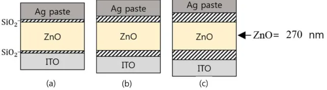
effort to further enhance the output voltage. As shown in Figure 2, the SZS-MGs are composed of a ZnO layer sandwiched between two SiO2 layers. In contrast, the ZSZ-MGs are composed of a silicon
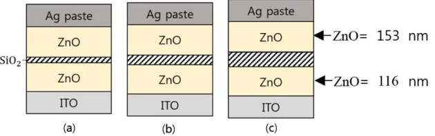
dioxide (SiO2) layer sandwiched between two ZnO layers, as shown in Figure 4. The ZnO layers were
deposited by sputtering for 1 h with an RF power of 200 W, resulting in an average thickness of 270 nm. The SiO2 layers were deposited by sputtering with an RF power of 200 W for 5, 15, and 30 min,
respectively. The output voltages were measured and compared to find out which device configurations could generate higher output voltages.
Figure 2. Schematic diagrams of three SZS-MGs with different SiO2 thin films(a) Upper SiO2 thickness = 78 nm, lower SiO2 thickness = 40 nm, (b) Upper SiO2 thickness = 90 nm, lower SiO2 thickness = 63 nm, (c) Upper SiO2 thickness = 146 nm, lower SiO2 thickness = 110 nm.
Figure 3. (a) Schematic diagram of control MG with a single ZnO layer used as a reference sample and (b) its output voltage variation (VP-P = ~ 0.7 mV) (ZnO film thickness = 273 nm).
Figure 4. Schematic diagrams of three ZSZ-MGs with different SiO2 thin films. (a) SiO2 thickness = 17 nm, (b) SiO2 thickness = 52 nm, (c) SiO2 thickness = 141 nm.
While the control MG device made up of a single layer of ZnO alone showed a relatively low output voltage of 0.7 mV, as shown in Figure 3, better output voltages were obtained from the ZnO/SiO2-stacked film devices, i.e., the SZS-MGs and ZSZ-MGs illustrated in Figures 2 and 4. This is
considered to be mainly due to the inserted SiO2 insulating layers. The measured output voltages of
the three SZS-MGs illustrated in Figure 2 are plotted in Figure 5. In the case of the devices with SiO2
films deposited for times in the range from 5 min to 30 min, they produced slightly better output voltages ranging from about 0.9 to 1.7 mV. This seems to suggest that the thicker SiO2 layers lead to
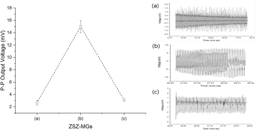
better output voltages, but the magnitude of the output voltage is still small. The measured output voltages of the three ZSZ-MGs shown in Figure 4 are plotted in Figure 6. The ZSZ-MGs showed output voltages about 9 times larger than those of the SZS-MGs. The ZSZ-MG device with a SiO2 film
interlayered between both the top and bottom ZnO layers was observed to generate about 15 mV of peak to peak (P-P) output voltage where the SiO2 film was deposited for 15 min. The deposition
conditions of ZnO and SiO2 thin films used for the SZS-MGs and ZSZ-MGs, mentioned respectively
Figure 5. (Left) Peak to peak (P-P) output voltages of three SZS-MGs as a function of the SiO2 deposition time. (Average deposition rate of SiO2 = 7.05 nm/min, ZnO = 4.55 nm/min at 200 W deposition power). (Right) Output voltage variations of the SZS-MGs with SiO2 thin films deposited for (a) 5 min, (b) 15 min, and (c) 30 min, respectively.
Figure 6. (Left) Peak to peak (P-P) output voltages of three ZSZ-MGs as a function of the SiO2 deposition time (Average deposition rate of SiO2 = 3.85 nm/min, ZnO = 4.48 nm/min at 200 W deposition power). (Right) Output voltage variations of three ZSZ-MGs with SiO2 thin films deposited for (a) 5 min, (b) 15 min, and (c) 30 min, respectively.
Table 1. Deposition conditions of ZnO and SiO2 thin films for both SZS-MGs and ZSZ-MGs shown in
Figures 5 and 6.
Film ZnO SiO2
Power (W) 200 200 Pressure (Torr) 1.0×10⁻² 1.0×10⁻²
Gas flow (sccm) N O (12) + Ar (18) Ar (20)
Substrate temperature (℃) 29 29 Target-substrate distance (cm) 12 12
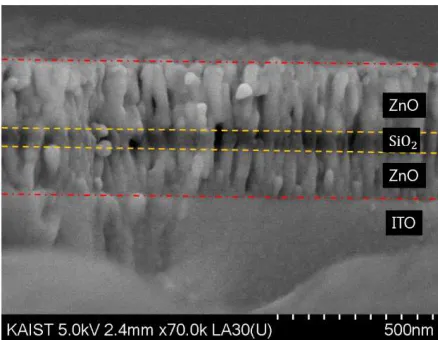
Figure 7. Cross-sectional SEM image of a typical ZSZ-MG sample fabricated in this work.
Table 2. Average thickness of each film layer in ZSZ-MGs in Figure 6. Time of SiO2 thin film deposition
(min) 5 15 30
Thickness of SiO2 thin film (nm) 17 52 141
Thickness of top ZnO thin film (nm) 153
Thickness of bottom ZnO thin film
(nm) 116
Therefore, the ZSZ-MGs showed better output voltages than the SZS-MGs after 300 bending/unbending cycles. Additionally, among the ZSZ-MGs, the SiO2 films deposited at 200 W for
15 min were of a desirable thickness, leading to the generation of the highest output voltages. This is believed to be due to the blockage of electrons. The two thicker SiO2 layers surrounding the ZnO
layer, as shown in Figure 2, can make it harder for electrons to flow into and out of the ZnO layer. This would suppress the screening effect while forming potential barriers, leading eventually to the elevation of the output voltage. On the other hand, when the SiO2 film is placed as an interlayer
between the top and bottom ZnO layers, as shown in Figure 4, there will be a critical or optimum thickness of the SiO2 film layer which acts as a barrier that helps to elevate the output voltage while
suppressing the screening effect. Moreover, a thinner SiO2 layer may allow relatively more electrons
to tunnel through the oxide film. If the SiO2 layer is thicker than the critical or optimum thickness, it
may more effectively block the tunneling of the electrons generated by the piezoelectric effect, thus reducing the net output voltage.
Table 2 shows the thicknesses of individual film layers. The SiO2 film thickness was about 52 nm
when the top ZnO film was 153 nm thick and the bottom one was 116 nm thick. Figure 7shows a cross-sectional view of the SiO2 layer sandwiched between the top and bottom ZnO layers. Since the
stacked ZnO and SiO2 layers are all oxide materials, they can be distinguished only by the contrast.
Both films show very similar growth orientation and morphology; the top layer is therefore affected by the bottom layer since they were epitaxially grown.
Comparing the output voltages of the SZS and ZSZ devices shown in Figures 5 and 6, the ZSZ devices were found to exhibit better performance than the SZS devices. From this observation, we were inspired to further investigate the ZSZ devices in the hope of enhancing the device performance even further. First, we investigated the effects of working pressure on the output voltages of the ZSZ devices. We fabricated five ZSZ-MG samples with SiO2 films deposited under various working
to peak (P-P) output voltages of these ZSZ-MGs with SiO2 thin films deposited under different
working pressures, indicating that there is a strong dependence of the output voltage on the working pressure during SiO2 film deposition. Table 3 summarizes the deposition conditions of both the ZnO
and SiO2 thin films used to fabricate these ZSZ-MGs. As shown in Figure 8, the ZSZ device with an
SiO2 film deposited for 15 min with an RF power of 200 W at working pressure of 5×10⁻² Torr
produced the best output performance (VP-P = 4.5 mV) among the five samples. As shown in Figure 9,
the surface and grain morphologies of the deposited SiO2 films seem to be affected by the working
pressure, which may eventually have an influence on the output voltage.
Figure 8. Peak to peak (P-P) output voltage variations of various ZSZ-MGs with different SiO2 thin
films deposited under different working pressures. Deposition power is fixed at 200 W.
Table 3. Deposition conditions of both ZnO and SiO2 thin films used to fabricate the ZSZ-MGs in
Figure 8.
Film ZnO SiO2
Power (W) 200 200
Pressure (Torr) 1.0×10⁻² 5.0×10⁻¹, 1.0×10⁻¹, 5.0×10⁻²,
1.0×10⁻², 5.0×10⁻³
Gas flow (sccm) N O (12) + Ar (18) Ar (20)
Substrate temperature (℃) 29 29
Target-substrate distance (cm) 12 12
Deposition time (min) 30 15
The SiO2 surface morphology appears to vary considerably depending on the working pressure.
The SEM images in Figure 9 show that the SiO2 grains became smaller and denser as the working
Figure 9. SEM images obtained at 200k times magnification showing the surface morphologies of the SiO2 thin films deposited under three different working pressures: (a) 5.0×10⁻¹, (b) 5.0×10⁻², and (c) 5.0×10⁻³ Torr. Deposition power was fixed at 200 W.
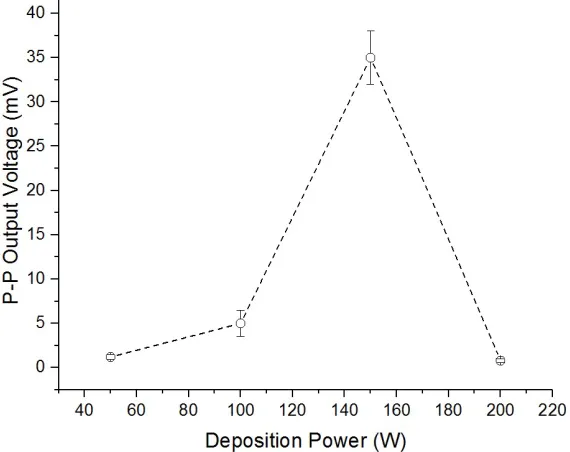
Second, we also investigated the effects of deposition power on the output voltage of the ZSZ-MGs devices. We fabricated four different ZSZ-MG devices with SiO2 films deposited using various
deposition powers of 50, 100, 150, and 200 W. The output voltage variations of those ZSZ-MGs are plotted in Figure 10. To maintain a similar thickness for each deposited oxide film, the deposition time alone was controlled to be inversely proportional to the applied RF power while keeping all other process conditions constant.
Figure 10. Peak to peak (P-P) output voltage variations of the ZSZ-MGs with SiO2 thin films deposited at various RF powers. Deposition working pressure was fixed at 1.0×10⁻² Torr.
The device measurements showed that the largest output voltage (35 mV) was generated by the ZSZ-MG device with a silicon dioxide (SiO2) thin film deposited using 150 W for 22.5 min, as shown
in Figure 10. This may be due to the formation at 150 W of the relatively fine-grained surface morphology shown in Figure 11. The deposition conditions of both ZnO and SiO2 thin films are
Table 4. Deposition conditions of both ZnO and SiO2 thin films used to fabricate the ZSZ-MGs in Figure 10.
Film ZnO SiO2
Power (W) 200 50, 100, 150, 200
Pressure (Torr) 1.0×10⁻² 1.0×10⁻²
Gas flow (sccm) N O (12) + Ar (18) Ar (20)
Substrate temperature (℃) 29 29 Target-substrate distance (cm) 12 12
Deposition time (min) 30 45, 30, 22.5, 15
Figure 11. SEM images obtained at 200k times magnification showing SiO2 thin films deposited using
various RF powers: (a) 50 W, (b) 100 W, (c) 150 W, and (d) 200 W.
4. Conclusions
Various ZnO/SiO2-stacked thin film structures were studied for flexible micro-energy harvesting
devices. Two types of micro-energy generators, ZSZ-MGs and SZS-MGs, were fabricated by stacking both SiO2 and ZnO thin films on top of each other using an RF magnetron sputtering technique, all
onflexible ITO-coated PEN substrates. The resulting devices were then characterized. In particular, the effects of SiO2 film thickness and position on device performance were investigated in terms of
the output voltage in comparison to a ZnO single-layer micro-energy generator used as a control device. Compared to the ZnO single-layer control device, the ZSZ-MGs showed much better output voltages while the SZS-MGs showed only slightly better output voltages. The output voltages of the ZSZ-MGs depended strongly on the working pressure during deposition of the SiO2 thin films. The
highest peak to peak (P-P) output voltage was about 34 mV obtained from the ZSZ-MG device where the SiO2 thin film was deposited at an RF power of 150 W. In the ZSZ or SZS devices with ZnO/SiO2
-stacked thin film structures, the output voltages were found to be significantly affected by the position and thickness of the SiO2 film layer(s) with respect to the ZnO layer(s) in addition to their
Author Contributions: Conceptualization, Investigation, Data Curation, Writing-Original Draft Preparation, Visualization, Yoon, C.; Equipment and Materials Managing and Preparation, Jeon, B. Writing-Review & Editing, Supervision, Yoon, G.;
Acknowledgments:This research was supported by Basic Science Research Program through the National Research Foundation of Korea (NRF) funded by the Ministry of Education (Grant No. 2016R1D1A1B01007074).
Conflicts of Interest: The authors declare no conflict of interest.
References
1. Chen, J.; Wang, Z. L. Reviving Vibration Energy Harvesting and Self-Powered Sensing by a Triboelectric Nanogenerator. Joule 2017, 1(3), 480-521. doi:10.1016/j.joule.2017.09.004.
2. Wang, X.; Song, J.; Liu, J.; Wang, Z. L. Direct-Current Nanogenerator Driven by Ultrasonic Waves. Science
2007, 316(5821), 102-105. doi:10.1126/science.1139366.
3. Yang, W.; Chen, J.; Zhu, G.; Yang, J.; Bai, P.; Su, Y.; Jing Q; Cao X; Wang Z. L. Harvesting Energy from the Natural Vibration of Human Walking. ACS Nano 2013, 7(12), 11317-11324. doi: 10.1021/nn405175z. 4. Chen, J.; Yang, J.; Li, Z.; Fan, X.; Zi, Y.; Jing, Q.; Guo, H.; Wen, Z.; Pradel, K. C.; Niu, S.; Wang, Z. L. Networks
of Triboelectric Nanogenerators for Harvesting Water Wave Energy: A Potential Approach toward Blue Energy. ACS Nano 2015, 9(3), 3324-3331. doi:10.1021/acsnano.5b00534.
5. Zhang, L.; Zhang, B.; Chen, J.; Jin, L.; Deng, W.; Tang, J.; Zhang, H.; Pan, H.; Zhu, M.; Yang, W; Wang, Z. L. Lawn Structured Triboelectric Nanogenerators for Scavenging Sweeping Wind Energy on Rooftops. Adv. Mater. 2015, 28(8), 1650-1656. doi:10.1002/adma.201504462.
6. Zhang, N.; Chen, J.; Huang, Y.; Guo, W.; Yang, J.; Du, J.; Fan, X.; Tao, C. A Wearable All-Solid Photovoltaic Textile. Adv. Mater. 2015, 201528(2), 263-269. doi:10.1002/adma.201504137.
7. Zi, Y.; Lin, L.; Wang, J.; Wang, S.; Chen, J.; Fan, X.; Yang, P.; Yi, F.; Wang, Z. L.Triboelectric–Pyroelectric– Piezoelectric Hybrid Cell for High‐Efficiency Energy‐Harvesting and Self‐Powered Sensing. Adv. Mater.
2015, 27, 2340. doi:10.1002/adma.201500121.
8. Olutade, B. L.; Hunt,W.D. Sensitivity Analysis of a Thin Film Bulk Acoustic Resonator Ladder Filter. IEEE Intl. Freq. Ctrl. Sym. 1997, p737. doi: 10.1109/FREQ.1997.638779.
9. Hinchet, R.; Lee, S.; Ardila, G.; Monte`s, L.; Mouis, M.; Wang, Z. L. J. Ener. Pow. Eng. 2013, 7, 1816.
10. Yang, R.; Qin, Y.; Dai, L.; Wang Z. L. Power generation with laterally packaged piezoelectric fine wires, Nat. Nanotechnol. 2008, 4, 34. doi:10.1038/nnano.2008.314.
11. Lee, M.; Chen, C.; Wang, S.; Cha, S.; Park, Y.; Kim, J.; Chou, L.; Wang, Z. L. A Hybrid Piezoelectric Structure for Wearable Nanogenerators, Adv. Mater. 2012, 24, 1759. doi:10.1002/adma.201200150.
12. Lee, E.; Park, J.; Yim, M.; Kim, Y.; Yoon, G. Characteristics of piezoelectric ZnO/AlN-stacked flexible nanogenerators for energy harvesting applications. Appl. Phys. Lett. 2015, 106, 023901. doi: 10.1063/1.4904270.
13. Lee, E.; Park, J.; Yim, M.; Jeong, S.; Yoon, G. High-efficiency micro-energy generation based on free-carrier-modulated ZnO:N piezoelectric thin films. Appl. Phys. Lett. 2014, 104, 213908. doi:10.1063/1.4880935. 14. Yin, B.; Qiu, Y.; Zhang, H.; Lei, J.; Chang, Y.; Ji, J.; Luo, Y.; Zhao, Y.; Hu, L. Piezoelectric performance
enhancement of ZnO flexible nanogenerator by a NiO-ZnO p-n junction formation. Nano. Ener. 2015, 14, 95-101. doi:10.1016/j.nanoen.2015.01.032.
15. Park, H.; Lee, K. Y.; Seo, J.; Jeong, J.; Kim, H.; Choi, D.; Kim, S. Charge-Generating Mode Control in High-Performance Transparent Flexible Piezoelectric Nanogenerators. Adv. Funct. Mater. 2011, 21, 1187-1193. doi:10.002/adfm.201002099.
16. Przezdziecka, E.; Chusnutdinow, S.; Guziewicz, E.; Snigurenko, D.; Stachowicz, M.; Kopalko, K.; Reszka, A.; Kozanecki, A. The p-ZnO:N/i-Al2O3/n-GaN heterostructure-electron beam induced profiling, electrical properties and UV detectivity. J.Phys. D: Appl.Phys. 2015, 48, 325105. doi:10.1088/0022-3727/48/32/325105. 17. Lee, K.Y.; Kumar, B.; Seo, J.; Kim, K.; Sohn, J.I.; Cha S.N.; Choi, D.; Wang, Z.L.; Kim, S. P-Type
Polymer-Hybridized High-Performance Piezoelectric Nanogenerators. Nano Lett. 2012, 12, 1959-1964. doi:10.1021/nl204440g