A Highly Efficient Carry Select Adder
Shiya Andrews V Jyothis Candran G
PG Student Assistant Professor
Department of Electronics & Communication Engineering Department of Electronics & Communication Engineering Saintgits College of Engineering Saintgits College of Engineering
Abstract
Design of high speed, area efficient and low power logic systems is the main challenge of VLSI system design. Adder circuit is the main building block of the digital system. But digital adders suffer with the problem of carry propagation delay. To deaden this problem, Carry Select Adder (CSLA) is used in computational circuit. In this paper, the logic operations involved in conventional CSLA, modified Binary To Excess-1 Converter (BEC) based CSLA and Common Boolean Logic (CBL) based CSLA are analysed to study the data dependencies and thereby identify and decimate the redundant logic operations. In the modified scheme, the carry select (CS) operation is done before the calculation of the final sum. The modified CSLA involves less area and delay than the CBL based CSLA.
Keywords: Adder, Arithmetic Unit, Low Power Design
________________________________________________________________________________________________________
I.
I
NTRODUCTIONElectronic devices have greatly decreased in size and mass over the few decades. Most of us carry or wear these electronic devices in our daily life. VLSI technology enjoyed the tremendous growth characterized by Moore‘s law. In VLSI design, researchers are interested greatly in the design of systems with high speed; less area and that are power efficient. Be it any processor, the data path pays a prominent role because the performance metrics like power dissipation, area, delay all directly depends on the data path. The data path involves complex computations and realizing hardware units for these paths is not an easy task. It must be done with prime importance. The most executed operation in the data path is addition and this requires a binary adder that adds two numbers. Adders also play a vital role in more complex computations like multiplication, division and decimal operations. Hence, an efficient implementation of binary adder is crucial to an efficient data path.
Adders form the basis of any circuit. A computational circuit is incomplete without an adder. The aim of these circuits is to reduce power consumption and delay. Therefore these binary adders are crucial building blocks of very large scale integrated circuits. Adders find its use in computers and processors and they are used not only in arithmetic logic units but also in other parts of the processors where they are used to calculate addresses, table indices, etc. Since an adder is widely used in VLSI design, the adder must be chosen in such a way that it do not affect the performance of the system as a whole. The speed of addition is limited by the time it requires for the carry to propagate through the adders. The sum for each bit position is generated sequentially and only when it is propagated to the next bit position the addition happens in that bit position. So the major speed limitation is in the generation of the carries. Many adder designs are available in literature. Ripple Carry Adder has got the simplest design but it has got less speed. Hence carry propagation delay is the main concern. Several methods have been suggested to reduce the carry propagation delay. Carry Select and Carry Look-ahead methods have been suggested.
The carry-select adder consists of two ripple carry adders and a multiplexer. Addition of two n-bit numbers with a carry-select adder is done using two adders that is here we use two ripple carry adders in order to perform the calculation twice, with the assumption of the carry being zero and one. The two results are calculated in parallel and the correct sum and the correct carry, is then selected with the multiplexer once the correct carry is known. A conventional carry select adder has got less carry propagation delay when compared to that of Ripple Carry Adder. Though it has got less carry propagation delay (CPD) the design is not as attractive as it uses dual Ripple Carry Adder (RCA). Several designs have been introduced in literature that avoids the use of dual RCA and thereby reducing the area occupied and power consumed.
The basic idea of this work is to use Binary to Excess-1 Converter (BEC) instead of RCA with cin = 1 in the regular CSLA to achieve lower area and power consumption. The main advantage of this BEC logic comes from the lesser number of logic gates than the n-bit Full Adder (FA) structure, but it has marginally higher delay. A CSLA based on common Boolean logic (CBL) is also designed. It has less CPD. However, the CBL-based SQRT CSLA design requires more logic resource and delay than the BEC-based SQRT-CSLA.
Based on the proposed logic formulation, we have derived an efficient logic design for CSLA. Due to optimized logic units, the proposed CSLA involves significantly less ADP than the existing CSLAs. The rest of this brief is organized as follows. A detailed description of different adders is dealt in Section II. The regular SQRT CSLA, BEC based CSLA and the CBL based CSLA is presented in Section III. The modified CSLA is given in Section IV and the experimental results and the performance comparison is given in Section V and finally the conclusion.
II.
L
ITERATURE REVIEWAdder also called as summer is a digital circuit that adds numbers and they finds its use in many processors and computers where they are used not only in arithmetic logic units, but they are also used in other parts of the processor where they are used to do numerous operations like calculate addresses, table indices, operations like increment and decrement and similar others. Adders normally operate on binary numbers. Addition is a crucial arithmetic function that determines the overall performance of the system. Adders are most widely used in electronic applications. So speed of the operation is the major constraint while we choose adders for the design of multipliers. Since we are going for portable devices, miniaturization of the design should be high and the power consumption should be low. An efficient adder design improves the performance of the design as a whole. In digital adders the speed of addition is limited by the time it takes for the carry to propagate through the adder. After the addition of the elementary bit position, the sum and the carry is generated and the carry is propagated to the next bit position and the addition happens again and this continues until all the carry get propagated through the adder. Ripple Carry Adder has got the most compact design of all but it has the longest computing time of all the adder designs. Carry Look ahead Adder is the fastest but it consumes more area. So as a compromise of the two we go for Carry Select Adder.
Ripple Carry Adders (RCA): A.
To add an N bit number, multiple full adder circuits can be cascaded in parallel. In a Ripple Carry Adder (RCA), the carry out of one full adder is given as the carry in of the succeeding next most significant full adder. It‘s called a ripple carry adder because the carry bits are rippled to the next stage.
Fig. 2.1: 4-Bit Ripple Carry Adder
Carry Look-ahead Adder (CLA): B.
A carry-look ahead adder improves speed by reducing the amount of time required to determine carry bits. The carry-look ahead adder calculates one or more carry bits before the sum, which reduces the wait time to calculate the result of the larger value bits. Carry look ahead logic uses the concepts of generating and propagating carries. Although in the context of a carry look ahead adder, it is most natural to think of generating and propagating in the context of binary addition, the concepts can be used more generally than this. In the descriptions below, the word digit can be replaced by bit when referring to binary addition of 2.
Carry Select Adder (CSLA): C.
Fig. 2.2: Basic Building Block F Carry Select Adder
Above is the basic building block of a carry-select adder, where the block size is 4. Two 4-bit ripple carry adders are multiplexed together, where the resulting carry and sum bits are selected by the carry-in. Since one ripple carry adder assumes a carry-in of 0, and the other assumes a carry-in of 1, selecting which adder had the correct assumption via the actual carry-in yields the desired result.
III.
E
XISTING DESIGNSBasic Structure Of Regular SQRT CSLA: A.
The CSLA is used in many computational systems to alleviate the problem of carry propagation delay by independently generating multiple carries and then select a carry to generate the sum. However, the CSLA is not area efficient because it uses multiple pairs of Ripple Carry Adders (RCA) to generate partial sum and carry by considering carry input Cin=O and Cin=I, then the final sum and carry are selected by the multiplexers (mux). The existing modified SQRT CSLA is to use Binary to Excess-I Converter (BEC) instead of RCA with Cin=1 in the regular CSLA to achieve lower area and power consumption with slightly increase in the delay.
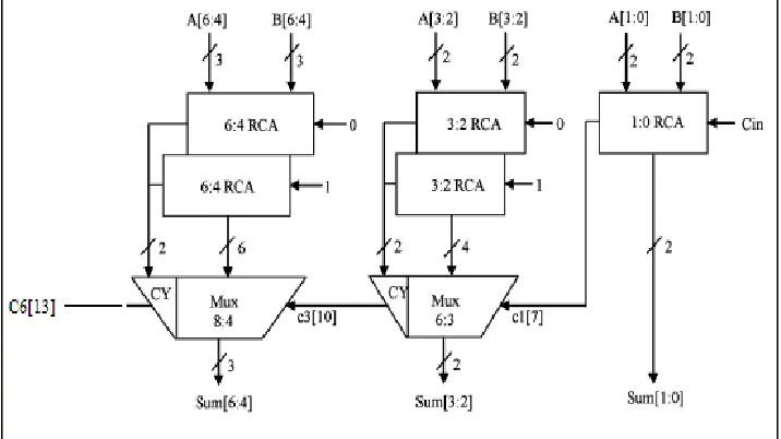
The basic square root Carry select adder has a dual ripple carry adder with 2: 1 multiplexer the main disadvantage of regular CSLA is the large area due to the multiple pairs of ripple carry adder. The regular 8-bit Carry select adder is shown in Fig. 1. It is divided into five groups with different bit size RCA. From the structure of Regular CSLA, there is scope for reducing area and power consumption.
The carry out calculated from the last stage i.e. least significant bit stage is used to select the actual calculated values of the output carry and sum. The selection is done by using a multiplexer. Internal structure of the group 3 of regular 8-bit CSLA is shown Fig.2.By manually counting the number of gates used for group 3 is 87 (full adder, half adder, and multiplexer) and 13ns delay. One input to the mux goes from the RCA with Cin=O and other input from the RCA with Cin=1.
TOTAL GATE COUNT=163
TOTAL NUMBER OF TRANSISTORS=364
Basic structure of BEC based CSLA: B.
The basic idea of this work is to use Binary to Excess-1 Converter (BEC) instead of RCA with Cin = 1 in the regular CSLA to achieve lower area and power consumption. The main advantage of this BEC logic comes from the lesser number of logic gates than the n-bit Full Adder (FA) structure.
The AND, OR, and Inverter (AOI) implementation of an XOR gate is shown in Fig. 3.2. The gates between the dotted lines are performing the operations in parallel and the numeric representation of each gate indicates the delay contributed by that gate. The delay and area evaluation methodology considers all gates to be made up of AND, OR, and Inverter, each having delay equal to 1 unit and area equal to 1 unit. We then add up the number of gates in the longest path of a logic block that contributes to the maximum delay. The area evaluation is done by counting the total number of AOI gates required for each logic block. Based on this approach, the CSLA adder blocks of 2:1 mux, Half Adder (HA), and FA are evaluated and listed in Table I.
Fig. 3.2: Delay and Area Evaluation of an XOR Gate
Table - 3.1
Delay and the Area Count of the Basic Blocks of CSLA
ADDER BLOCKS DELAY AREA
XOR 3 5
2:1 MUX 3 4
HALF ADDER 3 6
FULL ADDER 6 13
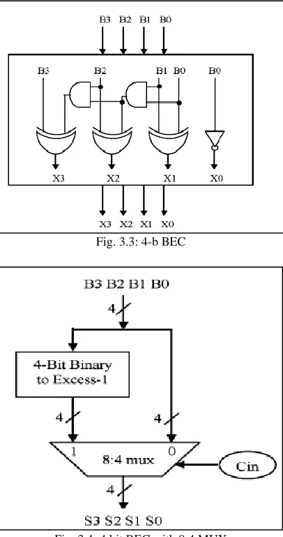
Fig. 3.3: 4-b BEC
Fig. 3.4: 4 bit BEC with 8:4 MUX
Thus, modified CSLA is designed such that it occupies less area and has low power than conventional CSLA. Block diagram of Modified CSLA is shown in Fig. 3.5.
Fig. 3.5: 8 bit BEC based CSLA
TOTAL GATE COUNT=128
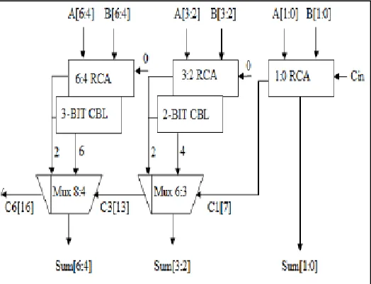
Basic structure of CBL based CSLA: C.
To remove the duplicate adder cells in the conventional CSLA, an area efficient SQRT CSLA is proposed by sharing Common Boolean Logic (CBL) term. While analysing the truth table of single bit full adder, results show that the output of summation signal as carry-in signal is logic ―0‖ is inverse signal of itself as carry-in signal is logic ―1‖. It is illustrated by red circles in able 3.2. To share the Common Boolean Logic term, we only need to implement a XOR gate and one INV gate to generate the summation pair. And to generate the carry pair, we need to implement one OR gate and one AND gate. In this way, the summation and carry circuits can be kept parallel.
Table - 3.2
Truth Table Of Single Bit Full Adder, Where The Upper Half Part Is The Case Of Cin = 0 And The Lower Half Part Is The Case Of Cin = 1
This method replaces the Binary to Excess-1 converter add one circuit by common Boolean logic. As compared with modified SQRT CSLA, the proposed structure is little bit faster. The transistor count is trade-off with the speed in order to achieve lower power delay product. Figure 3.6 shows the block diagram of CBL based CSLA.
Fig. 3.6: 8 bit CBL based CSLA
TOTAL GATE COUNT=99
TOTAL NUMBER OF TRANSISTORS=205
IV.
M
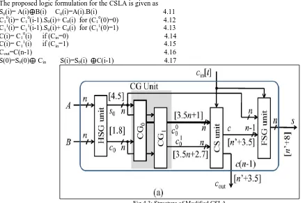
ODIFIED HIGHLY EFFICIENT CARRY SELECT ADDERLogic Formulation of Carry Select Adder: A.
The carry select adder has got two units, they are the sum and carry generator unit (SCG) and the sum and the carry selection unit. The SCG unit uses large number of logic resources and therefore it significantly contributes to the critical path. So it is the SCG unit that the concentration is to be on..
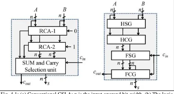
Fig. 4.1: (a) Conventional CSLA; n is the input operand bit-width. (b) The logic operations of the RCA is shown in split form, where HSG, HCG, FSG, and FCG represent half-sum generation, half-carry generation, full-sum generation, and
full-carry generation, respectively.
The SCG unit of the conventional CSLA [3] as shown in figure 1 (a) is composed of two n-bit RCAs, where n is the bit width of the adder. The logic operation of the n-bit RCA is performed in four different stages:
1) Half-Sum Generation (HSG); 2) Half-Carry Generation (HCG); 3) Full-Sum Generation (FSG); 4) Full-Carry Generation (FCG).
Consider the case when we go for the addition of two n –bit operands in conventional CSLA. The RCA-1 and RCA-2 generate sum and output carry which are n bit corresponding to input-carry (Cin = 0 and Cin = 1), respectively. Logic expressions that concerns the RCA-1 and RCA-2 of the SCG unit of the n-bit CSLA are given as
S00(i)=A(i) B(i) C00(i)=A(i).B(i) 4. 1
S1 0
(i)= S0 0(i) C
1 0
(i-1) 4.2 C10(i)= C00(i)+ S00(i). C10(i-1) C0out = C10(n-1) 4.3
S01(i)=A(i) B(i) C01(i)=A(i).B(i) 4.4
S11(i)= S01(i) C11(i-1) 4.5
C11(i)= C01(i)+ S01(i). C11(i-1) C1out = C11(n-1) 4.6
The logic expressions of the BEC unit of the n-bit BEC-based CSLA are given as S11(0)= S10(0) C11(0)= S10(0) 4.7
{ S11(i)= S10(i) C11(i-1) 4.8
C1(i)= S1 0
(i). C1 1
(i-1) 4.9 Cout1= C10(n-1) C11(n-1) 4.10
The proposed logic formulation for the CSLA is given as S0(i)= A(i) B(i) C0(i)=A(i).B(i) 4.11
C10(i)= C10(i-1).S0(i)+ C0(i) for (C10(0)=0) 4.12
C11(i)= C11(i-1).S0(i)+ C0(i) for (C11(0)=1) 4.13
C(i)= C10(i) if (Cin=0) 4.14
C(i)= C11(i) if (Cin=1) 4.15
Cout=C(n-1) 4.16
S(0)=S0(0) Cin S(i)=S0(i) C(i-1) 4.17
Fig 4.3: Structure of Modified CSLA
Proposed Design of Carry Select Adder: B.
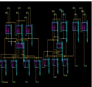
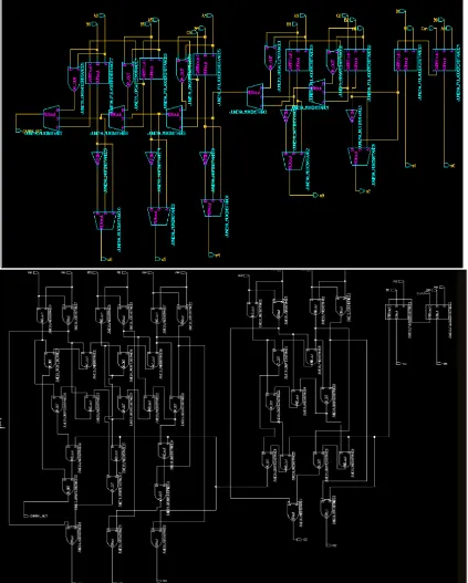
The proposed CSLA is based on the logic formulation given in (4.11 – 4.17), and its structure is shown in Fig. 3(a). It consists of one HSG unit, one FSG unit, one CG unit, and one CS unit. The CG unit is composed of two CGs (CG0 and CG1) corresponding to input-carry ‗0‘ and ‗1‘. he HSG receives two n-bit operands (A and B) and generate half-sum word s0 and half-carry word c0 of width n bits each. Both CG0 and CG1 receive s0 and c0 from the HSG unit and generate two n-bit full-carry words c01 and c11 corresponding to input-carry ‗0‘ and ‗1‘, respectively. he logic diagram of the HSG unit is shown in Fig. 3(b). The logic circuits of CG0 and CG1 are optimized to take advantage of the fixed input-carry bits. The optimized designs of CG0 and CG1 are shown in Fig. 3(c) and (d), respectively. The CS unit selects one final carry word from the two carry words available at its input line using the control signal cin. It selects c01 when cin = 0; otherwise, it selects c11. The CS unit can be implemented using an n bit 2-to-l MUX. However, we find from the truth table of the CS unit that carry words c01 and c11 follow a specific bit pattern. If c01 (i = ‗1‘, then c11 (i) = 1, irrespective of s0(i) and c0(i), for 0 <= i <= n − 1. This feature is used for logic optimization of the CS unit. The optimized design of the CS unit is shown in Fig. 3(e), which is composed of n AND–OR gates. The final carry word c is obtained from the CS unit. The MSB of c is sent to output as Cout, and (n − 1) LSBs are XORed with (n − 1) MSBs of half-sum (s0) in the FSG [shown in Fig. 3(f)] to obtain (n − 1) MSBs of final-sum (s). The LSB of s0 is XORed with Cin to obtain the LSB of s
.
TOTAL GATE COUNT=93
V.
E
XPERIMENTAL RESULTSFig 5.1: Simulation Setup of 8-bit Regular SQRT CSLA
Fig 5.3: Simulation Setup of CBL based 8-bit SQRT CSLA and Simulation Setup of Proposed Highly Efficient Carry Select Adder
Table – 2
Performance Analysis of Existing and Proposed design
8-bit SQRT CSLA 8-bit BEC based CSLA 8-bit CBL based CSLA 8-bit Prposed Highy Efficient CSLA
GATE COUNT 163 128 99 93
NUMBER OF TRANSISTORS 364 286 205 197
DELAY (ps) 301.58 355.2 311.6 283.69
VI.
C
ONCLUSIONPower, delay and area are the constituent factors in VLSI design that limits the performance of any circuit. This paper presents a simple approach to reduce the area, delay and power of CSLA architecture. Adders form the basis of any computational circuit. As such the square root carry select adder which has got less area when compared to the carry lookahead adder is chosen. A close look to the figure of carry select adder makes it evident that some modifications in the design can reduce the number of transistors and thereby reduce the power consumption and delay. Initial modification done was the BEC based carry select adder where the ripple carry adder with Cin =1 was replaced with the Binary – to –Excess 1 converter, thus avoiding the use of dual ripple carry adder. The reduced number of gates of this design offers a great advantage in the reduction of area and also the total power. By sharing the common Boolean logic (CBL) term, the duplicated adder cells in the conventional carry select adder is removed. This further reduced the area and power. The main objective of SQRT-CSLA design is to provide a parallel path for carry propagation that helps to reduce the overall adder delay. In the existing designs, logic is optimized without giving an y consideration to the data dependence. An analysis was done on logic operations involved in conventional and BEC-based CSLAs to identify redundant logic operations. In the proposed scheme, the CS operation is scheduled before the calculation of final-sum, which is different from the conventional approach. Carry words corresponding to input-carry ‗0‘ and ‗1‘ generated by the SL based on the proposed scheme follow a specific bit pattern, which is used for logic optimization of the CS unit. Fixed input bits of the CG unit are also used for logic optimization. Based on this, an optimized design for CS and CG units are obtained. Using these optimized logic units, an efficient design is obtained for the CSLA. The proposed CSLA design involves significantly less area and delay than the recently proposed BEC-based CSLA. Due to the small carry output delay, the proposed CSLA design is a good candidate for the SQRT adder.
R
EFERENCES[1] asant Kumar Mohanty, ― rea–Delay–Power Efficient Carry-Select dder‖, I ransactions On ircuits And Systems—II: Express Briefs, VOL. 61, NO. 6, June 2014
[2] . amkumar and Harish M Kittur,‖ Low-Power and Area- fficient arry Select dder‖, I ransactions On Very Large Scale Integration VLSI Systems, VOL. 20, NO. 2, February 2012
[3] O. J. edrij, ― arry-select adder,‖ I rans. lectron. omput., vol. -11, no. 3, pp. 340–344, Jun. 1962.
[4] Y. Kim and L.-S. Kim, ―64-bit carry-select adder with reduced area,‖ lectron. Lett., vol. 37, no. 10, pp. 614–615, May 2001.
[5] Y. He, C. H. hang, and J. Gu, ― n area-efficient 64-bit square root carry select adder for low power application,‖ in Proc. I Int. Symp. ircuits Syst., 2005, vol. 4, pp. 4082–4085.