Low Power Consumption in 11t SRAM Design
by using CMOS Technology
Amit Namdev#1, PareshRawat#2
# PG Student [VLSI], Dept. of ECE, Truba College of Science and Technology Bhopal, India
Abstract:- Ever since the concept of miniaturization took off, process voltage and temperature variations have become the prominent issues because of device scaling. Ranging from electronic devices like smart phones, tablets, multimedia devices like iPod to digital televisions, servers and networking SRAM is being used almost everywhere. It gives the scope of optimizing existing SRAM Topologies to meet the increasing market demand. In this paper CMOS technology is used for SRAM cells in different topology and a proposed 11T SRAM cell are analysed with the other (N)T SRAM cells Proposed circuit shows maximum saving of dynamic power in NB and RB is to 82.21% and 90.57% in 10T, maximum leakage power saving in NB and RB mode is 57.53%, 61.35% at 250C and 45.13%, 48.52 at 1100C in 9T SRAM. Proposed 11T is better in term of power, delay and stability than other existing circuits. Simulation is done by using HSPICE at 32nm CMOS technology in Not Biased (NB) and Reverse Biased (RB) mode with VDD =1V for fair comparison of results.
Keyword:- CMOS, Low power consumption, Shorter
Channel Effect, NB and RB mode.
I. Introduction
There are various approaches that are adopted to reduce power dissipation, like design of circuits with power supply voltage scaling, power gating and drowsy method. Lower power supply voltage reduces the dynamic power in quadratic fashion and leakage power in exponential way. But power supply voltage scaling results in reduced noise margin. Many SRAM arrays are based on minimizing the active capacitance and reducing the swing voltage. In sub-100nm region leakage
Currents are mainly due to gate leakage and sub threshold leakage current. High dielectric constant gate technology decreases the gate leakage current. Forward body biasing methods and dual Vt techniques are used to reduce sub threshold leakage current. In sub threshold SRAMs power supply voltage (VDD) is lower than the transistor threshold voltage (Vt) and the
sub threshold leakage current is the operating current. The energy loss during writing is more than the energy loss during reading in conventional SRAM since there is full swing of voltage in bit lines whereas the bit line voltage swing is very less during reading. It is known that the energy stored in the bit lines of the conventional SRAM is lost to ground in each write operation during „1‟ to „0‟ transition and this is the main source of energy loss. The power dissipated in bit lines represents about 60% of the total dynamic power consumption during a write operation. There is a powerful approach in which the energy stored in the bit line capacitance that is normally lost to ground is collected and pumped back into the source. This is known as energy recovery approach as shown in Figure 1.
Figure.1. Statistical butterfly curves of 6T SRAM
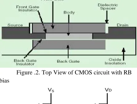
Figure .2. Top View of CMOS circuit with RB bias
VFG VRB VFG VRB
VS
VD
VD
VS
(a) (b) Fig.3 (a) 4T pCMOS device (b) 4T pCMOS device
Fig.3. represent pFinFET and nFinFET with, we consider two parallel transistors with two independent biasing front gate and back gate of FinFET technology. This two independent gate alter the threshold voltage of the transistor which mitigate leakage current. Table I, show drain current versus Front gate (
V
FG) voltage ofnCMOS, we varies the
V
FGand Revers body bias
voltage is kept constant (V
RB) from the table it is
observe that variation of the threshold voltage take
place I
OFFcurrent reduces drastically and I
ONcurrent
of
the
CMOS
device
increases
exponentially. It is calculate that V
RBbiasing is
more benefit for CMOS device and reduces the
sub-threshold current without degradation of
DIBL effect as shown in Table 1.
Table .I. Ids vs. VGS curve of nCMOS (W/L=80/32 nm)
V
FGI
dsV
RB=0
V
RB= -0.2
V
RB=-0.3
V
RB=-0.4
0
2.77E-08
5.31E-06
5.56E-06
5.56E-08
0.2
3.87E-05
3.87E-05
9.70E-05
2.63E-06
0.4
1.35E-04
9.70E-05
1.36E-04
5.02E-05
0.6
1.59E-04
1.11E-04
1.47E-04
7.23E-05
0.8
1.76E-04
1.20E-04
1.56E-04
8.25E-05
1
1.91E-04
1.27E-04
1.63E-04
9.06E-05
1.2
2.02E-04
1.34E-04
1.70E-04
9.77E-05
In this paper different topologies of SRAM cell are studied and proposed 11T SRAM cell on the basis of 6T SRAM, which is based on CMOS technology which improves read and write SNM characteristics and have lower leakage power. This paper is organized as challenges in the design of Standard SRAM circuits are reviewed in section II; this section specially gives an overview of the existing designs. The operation of the proposed SRAM design for low power and high speed operation is described in section III. Simulation results of existing and proposed techniques are presented in section IV. Finally the conclusion is given in section V.
2. Related Work
BL
M1
M2
M3
M4
(a)
W/L
BL
M1
M2
M3
M4 Vdd
GND
W/L
BL
M1
M2
M3
M4
Vdd
GND
BLB
M5 M6
(c)
W/L
BL
M1
M2
M3
M4 Vdd
GND
BLB
M5 M6
M7
(d)
W/L
BL
M1
M2
M3
M4 Vdd
GND
BLB
M5 M6
M7
M8
(e)
W/L
BL
M1
M2
M3
M4
Vdd
GND
BLB
M5
M6
M9 M11 M10
RD
(f)
W/L
BL
M1
M2
M3
M4 Vdd
GND
BLB
M5 M6
M7 M8
M9 M10
(g)
Fig.4. Schematics of (a) 4T SRAM (b) 5T SRAM (c) 6T SRAM (d) 7T SRAM (e) 8T SRAM (f) 9T SRAM (g) 10T SRAM. All circuit of SRAM cell is made by using CMOS technology.
bit line bar (BLB). When access transistors are switched on the memory elements can be accessed for read and write operation .Self aligned property of opposite gate of SRAM make this technology a better choice. Width can be used for reducing leakage current in SRAM along with supply voltage and threshold voltage but on contrary Vdd reduction leaves a strong impact on SRAM cell stability under parametric variations.
Three operation modes of SRAM Cell
Write mode - In this mode, cell can be written by different bit value simultaneously replacing its previous stored bit. To perform this operation, the access transistors (NM3 and NM4) are made enabled by using the word line (WL = 1). The required data which is to be written is given to the bit line (BL), and its complement value is applied on the bit line bar (BLB). That means if “1” is to be written , “1” to the bit line (BL) and zero “0” to the bit line bar (BLB) are assigned . When state of latch is changed this word line is deactivated (WL=0), and the required data is written to the SRAM cell.
Read mode - To read data from SRAM cell, the word
line (WL) is kept at high (WL=1) which makes the access transistors (NM3 and NM4) in active mode. Now for performing read operation, both bit lines are pre-charged to “1”. Depending on the state of the latch one bit will be in precharged stage and other will be in discharge. Now if bit line (BL) remains charged, the bit line bar (BLB) must be discharged or vice versa. Both these bit lines are applied at the input of the sense amplifier through which the information of the stored bit get amplified to a significant level at final stage.
Hold mode - SRAM cell is proficient of retaining the data till the time it is powered. If the word line (WL=0) is disabled, the access transistors become off and both bit line and the bit line bar (BLB) are detached from the latch. Now the two cross-coupled inverters will remain to reinforce each other till they are connected to (Vdd ) supply voltage and the current which is flowing is called leakage current.
In 7T SRAM Cell, the access transistors M5 is connected to the word-line (WL) , M7 is working as cascading back to back two inverters to reduce the delay as well as to decrease the power consumption and
M6 is connected to the RL (Read line) to perform the access write the read operations. In this way write operation depends only on one of the two bit lines which reduced the activity factor of discharging bit line pair. Other than that, there are several constraints on cell noise margin for trustworthy reading and writing operation is also affected. As the size of the device is scaled down, random process variations degrade the noise margin. If the size of the SRAM is goes to nanometer scale the variations in electrical parameters decreases due to the variations in process parameters i.e., density of impurity concentration, diffusion depths and oxide thickness.
Parameter Failures:
Mismatch in transistor strengths as a result of inter-die as well as intra-die process variation which means variation in width and length of transistors. The change in W/L ratio affects the drive capability of transistors and mismatch in driving capabilities lead to SRAM failure. LER (Line Edge Roughness) and RDF (Random Dopant Fluctuations) induced during fabrication process may also lead to failures for the same reason. These failures are of four types:
1. Destructive Read: While reading a value from the storage node in SRAM, sometimes the voltage of storing node go below or above trip point and as a result stored data is flipped.
2. Unsuccessful Write: Inability of imposed voltages on BL and BLB to overwrite the data (logic 0/1) of the storage node i.e. write failure. This may occur due to more write time due to less pulse width of Word line (which should be greater than critical pulse width) or inappropriately sized transistors.
3. Access Time failure: If more time is taken by SRAM cell to access storage node i.e sense the stored data, then this is termed as Access Time Failure. In this case, usually data is accessed during next cycle or more exceeding the delay requirements.
3. Proposed Work
In this paper we have proposed a new circuit of 11T SRAM shown in Figure .5. in the proposed circuit we have added two more PMOS transistor M8 and M9 that has been used in the PUN and transistor M10 PMOS sleep transistor and M11 NMOS pass transistor are placed above the PUN and Vdd both this transistor are parallel to each other. The main reason of the adding this transistor is to provide stacking by inserting additional PMOS transistors in PDN and sleep transistor PUN which leads in the voltage drop across the circuit. The NMOS transistor is placed parallel to the PMOS stack in pull down network called as evaluation transistor for mitigation of leakage power with scaling of technology. Therefore to calculate the leakage power in standby mode PDN in this PMOS stack which lead to the reduction of leakage current which in turn reduces the leakage power consumption in the circuit.
During read mode first of all BL is set to pre-charge high voltage (BL = „1‟), then the read operation is perform by special read word line (RWL), CBL turns high and the CBLB is turn to low voltage to turn off the transistor M7 and WL remains at high. From simulation result it observes that proposed 11T SRAM cell generates Q and QB output which depicts desirable waveform. In write operation pull down word line at low voltage (WL = „1‟) and set CBL signal at high voltage (CBL = „1‟), then LWL signal is pre-charged to high value (LWL = „1‟) then data writing operation perform from bit-line (BL) through M5 to the storage nodes (Q & QB). In hold mode, set the word line at high voltage (WL = „1‟) while read word line switch low (RWL = „1‟), hence transistor M5 & M6 turn off to prevent the access of bit line, CBLB is set high (CBLB = „1‟) to turn on transistor M7 as a result the same data retains in the cross coupled inverter pair. This design is most common because of its simplicity and compactness but the bits are adjacent to each other that cause the probability of multi-bit soft errors is very high. To solve the problem of soft errors the 2nd architecture i.e. bit interleaving architecture is used. A detailed explanation of bit-interleaving concept is explained.
W/L
BL
M1
M2
M3
M4
BLB
M6
CLK M7
M8
M9
S
M10 M11
Figure. 5.Proposed 11T SRAM
Figure.6. Transient analysis of proposed 11T SRAM cell
Figure .8. Standard Buttererfly Curve of Proposed 8T in RB mode FinFET
4. Results and Discussion
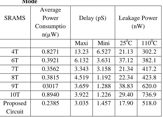
The simulated result is obtained by using HSPICE simulator at 32 nm in CMOS technology with 1V as supply voltage and 1pF output capacitance at 250C and 1100C temperature along with operating frequency of 100MHz. As leakage current reduces shorter channel effect (SCE) reduces, according to the simulation results in Table II saving of dynamic power dissipation in proposed circuit with existing circuit is 76.57% at 4T, 51.59% at 6T, 46.31% at 7T mode of CMOS Technology. In RB mode as shown in Table III saving of dynamic power dissipation in proposed circuit with existing circuit is 84.30% at 4T, 57.50% at 6T, 49.22% at 7T, 59.27% at 8T, 47.37% at 9T and 90.57% at 10T.Table.II Results of Proposed 11T SRAM Cell in NB Mode
SRAMS
Average Power Consumptio
n(µW)
Delay (pS) Leakage Power (nW)
Maxi Mini 250C 1100C 4T 0.8271 13.23 6.527 21.13 302.2 6T 0.3921 6.132 3.631 37.12 382.1 7T 0.3562 3.343 3.158 21.34 417.2 8T 0.3815 4.519 1.192 22.34 423.8 9T 03017 3.659 1.288 38.83 620.0 10T 0.8940 3.922 1.226 29.40 736.9 Proposed
Circuit
0.2385 3.035 1.457 17.90 518.0
Table.III. Results of Proposed 11T SRAM Cell in RB Mode
SRAMS
Average Power Consumptio
n(µW)
Delay (pS) Leakage Power (nW)
Maxi Mini 250C 1100C 4T 0.5363 21.12 9.764 17.23 521.3 6T 0.2623 9.143 4.761 29.04 612.4 7T 0.2342 5.453 3.568 15.35 498.5 8T 0.2667 6.226 0.681 18.46 503.3 9T 0.2035 5.271 0.284 32.37 711.2 10T 0.8262 5.461 0.899 26.31 634.4 Proposed
Circuit
0.0835 6.089 2.617 14.92 414.6
The power consumption in the circuit is mainly depends upon Supply voltage and number of elements. Power in the circuit is measured by measuring the voltage and current in each ranch. And the total power consumption is taking the average of this.
Figure.9. Average power consumption of existing and proposed SRAM cell
Figure.7 & 8 Shows the SNM curve of proposed circuit, Maximum Square drawn inside the SNM curve is Unity gain which is measure diagonally of the square. Figure.9 and 10 shows average power and Leakage consumptions at different temperature in existing and proposed circuit.
5. Conclusion
In this research paper, a novel 11T SRAM cell design for low leakage, high stability and improve read, write stability. The proposed circuit is based on 6T SRAM cell, which consist of footer transistor to reduce the static power with two cross coupled inverter. Proposed 11T SRAM cell the delay of the circuit is increased slightly at the voltages above 1.6V in comparison with that of standard 6T SRAM cell but PDP of the circuit significantly falls down at all the operating voltages. While significant reduction in both delay and power consumption is observed with respect to 9T SRAM. And proposed design is more stable and robust compared with the existing designs.
References
[1] K. Roy, S. Mukhopadhyay, H. Mahmoodi-meimand, “Leakage tolerant mechanisms and leakage reduction techniques in deep-submicron CMOS circuits”, In Proc. of IEEE, vol. 91, no. 2, pp. 305– 327, Feb 2003.
[2] Z. Chen, L. Wei, M. Johnson, and K. Roy, “Estimation of Standby Leakage Power in CMOS Circuits Considering Accurate Modeling of Transistor Stacks,” In Proc. of IEEE/ACM Design Automation Conference, 1998.
[3] A. Bansal, S. Mukhopadhyay, K. Roy, “Device-optimization technique for robust and low-power FinFET SRAM design in nanoscale,” IEEE Transactions on Electron Devices, vol 54, no.6, pp. 1409–1419, 2007.
[4] Seid Hadi Rasouli, Hamed F. Dadgour, Kazuhiko Endo, Hanpei Koike and Kaustav Banerjee,“Design Optimization of FinFET Domino Logic Considering the Width Quantization Property” IEEE TRANSACTIONS on Electron Devices, vol.57, no. 11, pp. 2934-2943, Nov 2010.
[5] Prateek Mishra, Anish Muttreja, and Niraj K. Jha. “FinFET Circuit Design” SPRINGER 2011
[6] Wen Wu, Mansun Chan, “Analysis of Geometry-Dependent Parasitics in Multifin Double-Gate FinFETs” IEEE TRANSACTIONS ON ELECTRON DEVICES, vol. 54, no. 4, pp. 692-698, APRIL 2007,
[7] E. Grossar et al., “Read stability and write-ability analysis of SRAM cells for nanometer technologies,” IEEE J. Solid-State Circuits, vol.41, no. 11, pp. 2577–2588, Nov. 2006.
[8]B.H. Calhoun and A.P. Chandrakasan, “A 256-kb 65-nm Subthreshold SRAM Design for Ultra-Low-Voltage Operation”, in Solid-State Circuits, IEEE Journal of, Volume 42, Issue 3, pp. 680 - 688, March 2007.
[9] Mayank Shastri, Shyam Akashe, “Read Write Stability With Leakage Minimization Of 4t Sram Cell For Nano Cmos Technology” in Proc. of IEEE, pp. 355-359, 2011.
[10] Anie Jain, Shyam Akashe, “Optimization of low power 7T SRAM cell in 45nm Technology” in Proc. of Advanced Computing & Communication Technologies IEEE, pp 324-327, 2012.
[11] K. Dhanumjaya, M. Sudha, M.N.Giri Prasad, Dr.K.Padmaraju, “Cell Stability Analysis of Conventional 6t Dynamic 8T Sram Cell In 45nm Technology” VLSICS, vol.3, no.2, pp. 41-51, April 2012.
[12] Hiroki Noguchi et al., “Which is the best dual port SRAM in 45nm process technology8T,10T single end and 10T differential” Renesas Technology corporation,2008.
[13] Zhiyu Liu, Volkan Kursun, " Characterization of a novel Nine Transistor SRAM cell,IEEE Transactions on Very Large Scale Integration Systems,voI. 46, Issue 4,pp-488-492, April 2008.
[14] Neil H.E.Weste,David Harris and Ayan Banerjee, “CMOS VLSI Design, a circuits and systems perspective” ,ISBN: 0321149017/9780321149015 Third edition, Pearson Education, 2005.