A BINARY TO EXCESS-1 CODE CONVERTER
TECHNIQUE TO DESIGN A LOW POWER AND
AREA EFFICIENT CARRY SELECT ADDER
Rachbathuni Harish
1, S.Vidyarani
2, L. Srinivas Reddy
21
M. Tech Scholar (VLSI), Nalanda Institute of Engg and Tech. (NIET),
Siddharth Nagar, Guntur, A.P. (India)
2
Associate. Professor (ECE), Nalanda Institute of Engg and Tech. (NIET),
Siddharth Nagar, Guntur, A.P. (India)
3
Assistant. Professor (ECE), Nalanda Institute of Engg and Tech. (NIET),
Siddharth Nagar, Guntur, A.P. (India)
ABSTRACT
Generally the fastest processing adders are used to perform fast arithmetic functions in many data processing
processors. Carry select adder (CSLA) is also comes under the fastest adders list. The structure of CSLA looks
simple and it reduces the main factors like area and power consumption. It uses an efficient gate-level
modification for the significant reduction in area and power consumption of Carry select adder. Newly 8-B,
16-B, 32-B and 64-B square root carry select adder (SQRT CSLA) architectures have been developed based this
new significant and efficient gate-level modification and compared those developed architectures with the
existed regular SQRT CSLA with slight increase in the delay. This is designed by using Verilog HDL and
synthesized on XILINX tool. The result of the proposed structure proves that it is better than regular existed
CSLA.
Keywords
—
CSLA, Binary to Excess One Logic, XOR Logic, Delay Calculation of BEC Logic
I.
INTRODUCTION
In VLSI to design a system, we need to satisfy the main factors of area, power consumption and speed. This is only the critical and achievable task for VLSI designer. In digital adders, the speed is limited where the carry generated from the addition must propagate through the addition, the addition of present two bits have to be wait until the completion of addition of previous bits and to get the carry from that previous addition. This CSLA can be widely used in many DSP systems because to make the computation easy by independently generating multiple carries and after that select a carry to generate sum. It takes more area for ripple carry adder (RCA) which generates partial sum and carries by considering Cin = 0 and Cin = 1.So, it won‘t be a efficient area
system. The final outputs sum and carry are selected by the multiplexers.
In the regular CSLA, the ripple carry adder is replaced by the Binary to Excess 1 converter (BEC) with Cin = 1
to achieve lower area and power consumption techniques. The main reason to get this idea of using BEC is the number of logic gates required is lesser than the n-bit full adder.
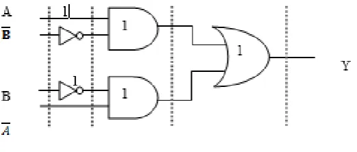
Fig 1: Delay and Area Evaluation of an XOR-Gate
II.
BASIC
ADDER
BLOCKS-AREA
AND
DELAY
EVALUATION
Implementation of XOR gate using AND, OR and NOT gates as structured in fig 1. In between dotted lines, have combination of logic gates runs the operation in parallel. The numbers expressed near gates are the delays have contributed by these gates. Coming to the delay and area evaluation, all the logic gates made up of AND, OR and NOT gates. The delay has declared as 1 unit and area also as 1 unit. Hare we add up the all AOI gates present in the longest path of a logic circuit to know the maximum delay of the circuit. The total number of AOI gates present in the logical block is declared as the area of that particular circuit. AOI represents AND, OR and Inverter gates.
Based on this criterion, the CSLA adder blocks of full adder (FA), half adder (HA) and 2:1 MUX has evaluated and listed below in TABLE I.
III.
STRUCTURE
AND
FUNCTION
OF
BEC
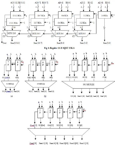
We have already discussed that BEC is using to decrease the area and power consumption of the regular CSLA replacing RCA with Cin = 1. Here we need to replace the n-bit RCA with n+1-bit BEC. The structure of 4-B
The basic function of the CSLA using BEC along with a multiplexer can be illustrated as in fig 3. One input is applied from any one of the B0, B1, B2, B3 and another one input is gets from the output of BEC output. Those two inputs of multiplexer are partial results and the multiplexer need to select one from it using selection line (control signal) Cin. The importance of BEC is the area of the design must reduces at great extend when we are
going to use large number of bits for design of CSLA.
The Boolean expressions of the 4-B Binary to Excess 1 converter as displayed below.
X0 = ~B0
X1 = B0 ^ B1
X2 = B2 ^ (B0 & B1)
X3 = B3 ^ (B0 & B1 & B2)
IV.
AREA
AND
DELAY
EVALUATION
OF
THE
REGULAR
16-B
SQRT
CSLA
(d)
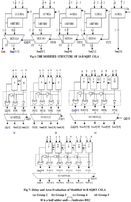
Fig 5: Delay and area evaluation of regular SQRT CSLA
Here, F indicates FULL ADDER
2. The arrival time of data outputs from the RCA‘s are always lower than the arrival time of MUX selection input except one group i.e., Group 2. The delay of all groups except Group 2 have displayed below as follows respectively.
{C6, Sum [6:4]}= C3 [t = 10] + MUX
{C10, Sum [10:7]}= C6 [t = 13] + MUX
{Cout, Sum [15:11]}= C10 [t = 16] + MUX
3. In Group 2, one set of 2-B RCA has 2 full adders for Cin = 1 and the other set has one full adder and one half
adders for Cin = 0. The total number of gate counts has determined below based on Table I, contained area count.
Gate count = 57 (FA + HA + MUX) FA = 39 (3*13)
HA = 6 (1*6) MUX = 12 (3*4)
and later than the s2 (time = 4). Thus, the output sum3 is depends on s3 and MUX and coming to c3 (output from the MUX) is depends upon the partial c3 (input to the MUX) and MUX. Finally the sum2 depends on c1 and MUX.
2. The arrival time of selection input of MUX is always greater than the arrival time of other inputs from the BEC. From this it is clear that the delay of remaining groups except groups is depends on the arrival of MUX selection input and the MUX delay.
3. The area evaluation of Group 2 has stated below:
Gate count = 43 (FA + HA + MUX + BEC) FA = 13 (1*13)
HA = 6 (1*6) AND = 1 NOT = 1 XOR = 10 (2*5) MUX = 12 (3*4)
Fig 7: Delay and Area Evaluation of Modified 16 B SQRT CSLA
(a) Group 2 (b) Group 3 (c) Group 4 (d) Group 5
Carry Select Adder With BEC LOGIC:
VII. CONCLUSION
In this paper we are presenting a new method of carry select adder which reduces power. While adding higher orbits,we are using the excess one converter to reduce the hardware complexity. This adder is designed using Verilog HDL and synthesised in Xilinx ISE 13.2i
VIII. REFERENCES
[1] O. J. Bedrij, ―Carry-select adder,‖ IRE Trans. Electron. Comput., pp. 340–344, 1962.
[2] B. Ramkumar, H.M. Kittur, and P. M. Kannan, ―ASIC implementation of modified faster carry save adder,‖ Eur. J. Sci. Res., vol. 42, no. 1, pp. 53–58, 2010.
[4] Y. Kim and L.-S. Kim, ―64-bit carry-select adder with reduced area,‖ Electron. Lett., vol. 37, no. 10, pp. 614–615, May 2001.
[5] J. M. Rabaey, Digtal Integrated Circuits—A Design Perspective. Upper Saddle River, NJ: Prentice-Hall, 2001.
[6] Y. He, C. H. Chang, and J. Gu, ―An area efficient 64-bit square root carry-select adder for lowpower applications,‖ in Proc. IEEE Int. Symp. Circuits Syst., 2005, vol. 4, pp. 4082–4085.
[7] Cadence, ―Encounter user guide,‖ Version 6.2.4, March 2008.
AUTHOR DETAILS
RACHABATHUNI HARISH, Pursuing M.tech (VLSI) from Nalanda institute Of
Engineering and Technology (NIET), Siddharth Nagar, Kantepudi village, satenepalli
Mandal, Guntur Dist., A.P, INDIA His area of interest include low power and low area VLSI applications
S.VIDYARANI, she received master degree in VLSI. Her area of interest include Low
power VLSI system design. Currently she is working as Associate professor (ECE) from Nalanda institute of Engineering and Technology (NIET), Siddharth Nagar, Kantepudi village, Satenepalli Mandal, Guntur Dist, A.P,
L.SRINIVAS REDDY, He completed his post-graduation in DECS. His area of
interest includes digital electronics, digital communication, digital system design and VLSI technology and design. His research areas are optimal communication technology. He is currently working as Asst.professor (ECE) from Nalanda institute of
Engineering and Technology (NIET), Siddhartha Nagar, Kantepudi village, Satenepalli