Available online: https://edupediapublications.org/journals/index.php/IJR/ P a g e | 53
Analysis and Design of Ky And Sepic Converter For Solar Energy
Conversion With Mppt Controller
ARAVIND.N, M.Tech (Power System Engineering), PRIST University, Thanjavur,
ABSTRACT
In this project the design and
performance of a low power stand-alone solar photovoltaic (PV) energy generating system with SEPIC is to be investigated.. Due to the high system efficiency and the ability to operate with a wide variable input voltage, the proposed converter is an attractive design for alternative low dc voltage energy sources, such as solar photovoltaic modules and fuel cells.
A non isolated dc–dc converter with a high boost ratio would be advantageous for a two-stage PCS because it can be easily integrated with current PV systems while reducing the cost and maintaining a high system efficiency. Due to the different output voltages from the PV panel, it would be beneficial to have a system with a high efficiency over the entire PV voltage range to maximize the use of the PV during different operating conditions.
Another important function of the dc– dc converter for PV applications is being able to implement maximum power point tracking (MPPT). The ability to implement MPPT for an individual PV panel would ensure that a large cluster of PV could maintain maximum power output from each panel without interfering with the other panels in the system. The major consideration for the main power stage of the converter in being able to implement an accurate MPPT is that the input current ripple of the converter has to be low.
Key Words : power stand-alone solar
photovoltaic, SEPIC, maximum power point tracking
INTRODUCTION
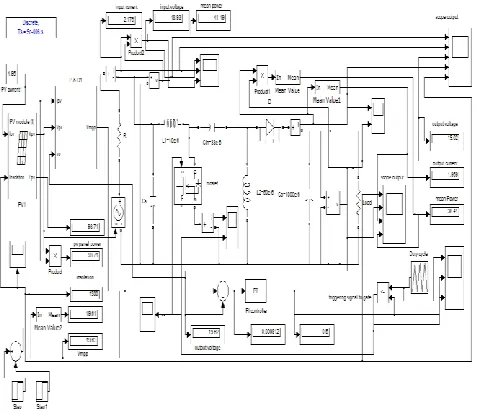
This project presents a non isolated, high boost ratio hybrid dc–dc converter with applications for low-voltage renewable energy sources The system is designed considering solar-PV panels of 750W to feed an average load demand of 250W for a rural household. The system includes series-parallel combination of solar panels, MPPT (maximum power point tracking) controller, a dc-dc SEPIC converter, an energy storage system .A dc-dc converter is providing a constant dc bus voltage and its duty cycle is controlled by the MPPT controller. A P&O approach is utilized for MPPT. In this
approach, MPPT controller automatically
generates a PWM signal for the dc-dc converter to extract maximum power. To maintain the power quality a feedback control is used. The complete system is designed, and modeled to evaluate its performance. Simulated results are presented to demonstrate the performance of the MPPT controller and designed system for
varying atmosphere conditions and load
disturbances.
Available online: https://edupediapublications.org/journals/index.php/IJR/ P a g e | 54
stress of a classical boost converter, a sepic-integrated boost (SIB) converter, which provides an additional step-up gain with the help of an isolated KY converter, is proposed. Moreover, the SIB converter needs no current snubber for the diodes, since the transformer leakage
inductor alleviates the reverse recovery. By
properly selecting a converter for a series output module, many advantages, such as high step-up capability, design flexibility, and distributed voltage stress can be achieved.
ANALYSIS OF SEPIC converter:
The Single-ended primary-inductor converter (SEPIC) is a type of DC-DC converter allowing the electrical voltage at its output to be greater than, less than, or equal to that at its input, the output of the SEPIC is controlled by the duty cycle of the control switch.
A SEPIC is similar to a usual buck-boost converter, but has advantages of having non-inverted output, the output voltage is of the same polarity as the input voltage, the isolation between its input and output and true shutdown mode. SEPICs are useful in applications in which a battery voltage can be above and below that of the regulator's intended output. The SEPIC converter uses two inductors ,one capacitor with a switch. The SEPIC exchanges energy between the capacitors and inductors in order to convert from one voltage to another. The amount of energy exchanged is controlled by switch S1, which is a MOSFET. The MOSFETs offer much higher input impedance and lower voltage drop and do not require biasing resistors because MOSFET switching is controlled by differences in voltage rather than a current
The main advantages of this converter are the continuous output current, smaller output voltage ripple, and lower semiconductors current stress compared with the conventional converter. By properly selecting a converter for a series output module, many advantages, such as high step up capability, design flexibility, and distributed voltage stress can be achieved.The Basic topology of SEPIC converter is shown in Fig2.
It can be operated on two modes:
Continuous current mode
Discontinuous current mode
Modeling of Solar-PV Array
Available online: https://edupediapublications.org/journals/index.php/IJR/ P a g e | 55
characteristics of the equivalent solar cell circuit can be expressed as,
Ipv = Iph – Ir [exp{ 𝑞
𝐴𝐾𝑇 (𝑉𝑝𝑣 +
𝐼 𝑝𝑣 𝑅𝑠)} –1 (1)
where Ipv is the output current from the
PV array, Vpv is the output voltage of the PV array, Iph is the photo generated current of the PV cell, Ir is the reverse saturation current of the diode, q is the electronic charge, A is the ideality factor, K is the Boltzman constant, T is the operating temperature of the cell and Rs is the internal resistance of the cell. From the Eq.(1) the PV cell is modeled in Simulink. The effect of variation in solar radiation is obtained through the model and shown in Fig. 4.From Fig. 4 it is confirmed that the solar-PV output power is function of the input solar radiation. The operating curves under different levels of the radiation show maximum output power points.
Sub Circuit of PV Module
Various MPPT technologies
Controllers usually follow one of three types of strategies to optimize the power output of an array. Maximum power point trackers may implement different algorithms and switch
between them based on the operating conditions of the array.[5]
Various MPPT technologies Hill climbing /
Perturbation & observation
Incremental conductance method
Fractional open circuit voltage
Fractional short circuit current
Fuzzy logic control Neural network
Ripple Correlation Control Current sweep Dc link capacitor droop
control, Load I or V maximization
dP/dV or dP/dI feedback
contr Array reconfiguration
Linear current control State based MPPT
One Cycle Control method Best fixed Voltage
SLIDE control Linear reoriented
coordinates method
Simple Flow chart of the MPPT algorithm Fig5.
Available online: https://edupediapublications.org/journals/index.php/IJR/ P a g e | 56 A. Hill Climbing/P&O
Among all the methods, much focus has been on hill climbing and perturb and observe (P&O) methods. Hill climbing involves a perturbation in the duty ratio of the power converter, and P&O a perturbation in the operating voltage of the PV array. In the case of a PV array connected to a power converter, perturbing the duty ratio of power converter perturbs the PV array current and consequently perturbs the PV array voltage. it can be seen that incrementing (decrementing) the voltage increases (decreases) the power when operating on the left of the MPP and decreases (increases) the power when on the right of the MPP. Therefore, if there is an increase in power, the subsequent perturbation should be kept the same to reach the MPP and if there is a decrease in power, the perturbation should be reversed.. This algorithm also works when. Instantaneous (instead of average) PV array voltage and current are used, as long as sampling occurs only once in each switching cycle. The process is repeated
periodically until the MPP is reached. The system then oscillates about the MPP. The oscillation can be minimized by reducing the perturbation step size.
KY Converter:
KY converter, a non- isolated DC-DC boost produces low output voltage ripple than the conventional class of converters. Besides, the output current is non pulsating, thereby causing the low output voltage ripple. Above all, its behavior is similar to that of the buck converter with synchronous rectification (SR), and hence, this converter possesses good load transient
response In addition, it possesses the non
pulsating output current, thereby not only decreasing the current stress on the output capacitor but also reducing the output voltage ripple. Furthermore, it has the positive output voltage, different from the negative output voltage of the traditional buck–boost converter. Such a converter has continuous input and output inductor currents, different from the traditional SR boost converter, and has a larger voltage conversion ratio than the traditional SR boost converter does, and hence, this converter is very suitable for low-ripple applications.
Available online: https://edupediapublications.org/journals/index.php/IJR/ P a g e | 57
SEPIC INPUT & OUTPUT PARAMETERS AT VARIOUS INSOLATION LEVELS WITH FIXED LOAD AND DUTY CYCLES
DUTY CYCLE=5KHZ LOAD R=10Ω
S.NO INSOL AT IO N (W / M 2) PV VOL T AGE IN VOL T S PV C UR R E NT IN AM PS PV PO W E R IN W AT T S
1 1000 17.66 4.95 85.14
2 1250 19.41 4.95 93
3 1500 18.7 4.95 95.78
TABLE 1 – SHOWS PV PARAMETERS AT VARIOUS INSOLATION LEVEL
SEPICCONVERTER INPUT & OUTPUT AT INSOLATION LEVEL 1250
CONCLUSION
B. Experimental Results
To verify the SIB converter, the prototype is implemented. The specification and design parameters obtained from the design example Fig. shows the key experimental waveforms at a full load condition and the overall waveforms are agreed well with the theoretical analysis. It is shown that the voltage
stresses on switch Q and diode Do1 are limited to
the output of boost converter Vo1 , which is
slightly higher than 100 V, neglecting the voltage spike caused by the parasitic inductance, though
VO is 20 V. There is no reverse recovery on IDo
1 , since it has an extremely low-current slope, i.e., ZCS turn-OFF is achieved. The current drop
on Ilkg at the switch turn-OFF transition can be
seen in Fig and its corresponding built-up current
can be found from IDo 2 in Fig. ILb, which
represents the input current is continuous the measured efficiency according to the load variation. Since the SIB converter employs low-voltage rating switch and diode, i.e., high
0 0.05 0.1 0.15 0.2 0.25 0.3 0.35 0.4 0.45 0.5 10 20 30 TIME V O L T A G E input voltage
0 0.05 0.1 0.15 0.2 0.25 0.3 0.35 0.4 0.45 0.5 0 5 10 TIME C U R R E N T input current
0 0.05 0.1 0.15 0.2 0.25 0.3 0.35 0.4 0.45 0.5 0 20 40 TIME V O L T A G E output voltage
0 0.05 0.1 0.15 0.2 0.25 0.3 0.35 0.4 0.45 0.5 -10 0 10 TIME C U R R E N T output current
Available online: https://edupediapublications.org/journals/index.php/IJR/ P a g e | 58
performance and low cost device, and the reverse recovery problem is considerably reduced.The SIB converter can achieve a high-voltage gain with the additional step-up ability of the isolated sepic converter and distributed voltage stress, while maintaining the advantages of the boost converter, such as a continuous input current and a clamped voltage stress on switch. Moreover, the reverse recovery problem is well suppressed, since the transformer leakage inductance alleviates a di/dt ratio of the turn-OFF diode current without additional snubber and the voltage stress on the secondary diode is limited by the clamp diodes. Therefore, the SIB converter is promising for nonisolated high step-up applications with simple structure and high efficiency. It is noted that other converters, REFERENCES
[1] Ki-Bum Park, Student Member, IEEE, Gun-Woo Moon, Member, IEEE,and Myung-Joong Youn, Senior Member, IEE “ Nonisolated High Step-up Boost Converter Integrated With Sepic
Converter” IEEE TRANSACTIONS ON
POWER ELECTRONICS, VOL. 25, NO. 9, SEPTEMBER 2010
[2] Jae-Won Yang and Hyun-Lark Do 3388 “Bridgeless SEPIC Converter With a Ripple- Free Input Current” IEEE TRANSACTIONS ON POWER ELECTRONICS, VOL. 28, NO. 7, JULY 2013
[ 3] Bin Gu, Student Member, IEEE, Jason Dominic, Jih-Sheng Lai, Fellow, IEEE, Zheng Zhao, Student Member, IEEE,and Chuang Liu, Student Member, IEEE2048 “High Boost Ratio
Hybrid Transformer DC–DCConverter for
Photovoltaic Module Applications” IEEE
TRANSACTIONS ON POWER
ELECTRONICS, VOL. 28, NO. 4, APRIL 2013 [4] Moacyr Aureliano Gomes de Brito, Luigi
Galotto, Jr., Leonardo Poltronieri
Sampaio,Guilherme de Azevedo e Melo, and Carlos Alberto Canesin, Senior Member, IEEEuan Lu, Senior Member“Evaluation of the
Main MPPT Techniques forPhotovoltaic
Applications”, IEEE 1156 IEEE
TRANSACTIONS ON INDUSTRIAL
ELECTRONICS, VOL. 60, NO. 3, MARCH 2013
[5] M. Salhi, R. El-BachtiriFaculty of Science Dhar El-Mehraz, Department of Physics, LESSI laboratory, REEPER groupEST, km5, Rte Immouzer, BP 2427, Fès, Morocco “Maximum Power Point Tracking Controller for PV Systems using a PIRegulator with Boost DC/DC Converter” ICGST-ACSE Journal, ISSN 1687-4811, Volume 8, Issue III, January 2009
[6] Ahmad J. Sabzali, Member, IEEE, Esam H. Ismail, Senior Member, IEEE,“Mustafa A. Al-Saffar, Member, IEEE, and Abbas A. Fardoun, Senior Member, IEEE New Bridgeless DCM Sepic and Cuk PFC Rectifiers With Low
Conduction and Switching Losses”IEEE
TRANSACTIONS ON INDUSTRY
APPLICATIONS, VOL. 47, NO. 2,
MARCH/APRIL 2011 873
[7] Hyun-Lark Do “ Soft-Switching SEPIC Converter With Ripple-Free Input Current” IEEE
TRANSACTIONS ON POWER