Volume 2006, Article ID 60613, Pages1–18 DOI 10.1155/ASP/2006/60613
Multiple-Clock-Cycle Architecture for the VLSI Design
of a System for Time-Frequency Analysis
Veselin N. Ivanovi´c, Radovan Stojanovi´c, and LJubiˇsa Stankovi´c
Department of Electrical Engineering, University of Montenegro, 81000 Podgorica, Montenegro, Yugoslavia
Received 29 September 2004; Revised 17 March 2005; Accepted 25 May 2005
Multiple-clock-cycle implementation (MCI) of a flexible system for time-frequency (TF) signal analysis is presented. Some very important and frequently used time-frequency distributions (TFDs) can be realized by using the proposed architecture: (i) the spectrogram (SPEC) and the pseudo-Wigner distribution (WD), as the oldest and the most important tools used in TF signal analysis; (ii) the S-method (SM) with various convolution window widths, as intensively used reduced interference TFD. This architecture is based on the short-time Fourier transformation (STFT) realization in the first clock cycle. It allows the mentioned TFDs to take different numbers of clock cycles and to share functional units within their execution. These abilities represent the major advantages of multicycle design and they help reduce both hardware complexity and cost. The designed hardware is suitable for a wide range of applications, because it allows sharing in simultaneous realizations of the higher-order TFDs. Also, it can be accommodated for the implementation of the SM with signal-dependent convolution window width. In order to verify the results on real devices, proposed architecture has been implemented with a field programmable gate array (FPGA) chips. Also, at the implementation (silicon) level, it has been compared with the single-cycle implementation (SCI) architecture.
Copyright © 2006 Hindawi Publishing Corporation. All rights reserved.
1. INTRODUCTION AND PROBLEM
FORMULATION
The most important and commonly used methods in TF sig-nal asig-nalysis, the SPEC and the WD, show serious drawbacks: low concentration in the TF plane and generation of cross-terms in the case of multicomponent signal analysis, respec-tively, [1–3]. In order to alleviate (or in some cases com-pletely solve) the above problems, the SM for TF analysis is proposed in [4]. Recently, the SM has been intesively used, [5–8]. Its definition is [4,9,10]
SM(n,k)
= Ld(n,k)
i=−Ld(n,k)
P(n,k)(i) STFT(n,k+i) STFT∗(n,k−i),
(1)
where STFT(n,k)=N/2
i=−N/2+1 f(n+i)w(i)e−j(2π/N)ik
repre-sents the STFT of the analyzed signal f(n), 2Ld(n,k) + 1 is the width of a finite frequency domain (convolution) rectangular windowP(n,k)(i) (P(n,k)(i)=0, for|i|> Ld(n,k)),
and the signal’s duration is N=2m. The SM produces, as its marginal cases, the WD and the SPEC with maximal (Ld(n,k)=N/2), and minimal (Ld(n,k)=0) convolution window width, respectively. In the case of a multicomponent
signal with nonoverlapping components, by an appropriate convolution window width selection, the SM can produce a sum of the WDs of individual signal components, avoiding cross-terms [4,10,11]:P(n,k)(i) should be wide enough to
enable complete integration over the auto-terms, but nar-rower than the distance between two auto-terms. In addi-tion, the SM produces better results than the SPEC and the WD, regarding calculation complexity [4] and noise influ-ence [9]. Note that the essential SM properties are: the high auto-terms concentration, the cross-terms reduction and the noise influence suppression.
Two possibilities for the SM (1) implementation are
(1) with a signal-independent (constant) Ld(n,k), Ld(n, k)=Ld=const, [4,10], when, in order to get the WD for each component, the convolution window width should be such that 2Ld+ 1 is equal to the width of the widest auto-term. For the entire TF plane, except at the central points of the widest component, this window would be too long. This fact might have negative ef-fects regarding cross-terms reduction, [4,10] and the noise influence suppression, [9]. On the other hand, the shorter window would result in lower concentra-tion;
disadvantages of the signal-independent form in the analysis of multicomponent signals having different widths of the auto-terms. In addition, it may fur-ther significantly improve the essential SM properties, [9,11].
In order to improve concentration of highly nonstation-ary signals, higher-order TFDs can be used [5,12]. One of them, which can be presented in a two-dimensional TF plane and defined in the same manner as the SM, is the L-Wigner distribution (LWD) [12]:
LWDL(n,k)= Ld
i=−Ld
LWDL/2(n,k+i) LWDL/2(n,k−i),
(2)
where LWDL(n,k) is the LWD of the Lth order, and LWD1(n,k) ≡ SM(n,k). Note that the LWD is implicitly
defined based on the SM and the STFT, so it can be imple-mented in a similar way as the SM.
Definition (1), based on STFT, makes the SM very at-tractive for implementation. However, all TFDs, beyond the STFT, are numerically quite complex and require significant calculation time. This fact makes them unsuitable for real-time analysis, and severely restricts their application. Hard-ware implementations, when they are possible, can overcome this problem and enable application of these methods in nu-merous additional problems in practice. Some simple imple-mentations of the architectures for TF analysis are presented in [10,13–19]. An architecture for VLSI design of systems for TF analysis and time-varying filtering based on the SM is presented in [16,17]. However, all these architectures give the desired TFD in one clock cycle. It means that no archi-tecture resource can be used more than once, and that any element needed more than once must be duplicated. Con-sequently, practical realization of these architectures requires large chips. Besides, just a single TFD—SM with exactly de-fined convolution window width—can be realized this way.
In this paper, we develop an MCI of a special purpose hardware for TF analysis based on the SM, suitable for the VLSI design. In the proposed implementation, each step in the TFDs execution will take one clock cycle. In the first step, proposed architecture realizes the STFT, as a key interme-diate step in realization of the implemented TFDs. In each higher-order clock cycle, different TFD is realized: in the sec-ond one—the SPEC, in the third one—the SM with unitary convolution window width, and so on. The WD is realized in the clock cycle when the maximal convolution window width is reached. Note that proposed architecture can real-ize almost all commonly used TFDs. The MCI design allows a functional unit to be used more than once per TFDs execu-tion, as long as it is used on different clock cycles. This sig-nificantly reduces the amount of the required hardware. The ability to allow TFDs to take different number of clock cycles and the ability to share functional units within the execution of a single TFD are the major advantages of the proposed de-sign.
The paper is organized as follows. After the intro-duction, MCI architectures for the SM realization (in its
signal-independent and signal-dependent forms) are de-signed, the corresponding controls are defined, and the trade-offs and comparisons with the SCI are given. In Section 3, the designed MCI system is used for the real-time realization of the higher-order TFDs. The proposed ap-proaches are verified in Section 4 by designing the FPGA chips. Also, the obtained implementation results at silicon level are compared with SCI architectures.
2. MULTICYCLE HARDWARE IMPLEMENTATION
OF THE S-METHOD
2.1. Signal-independent S-method
In this section, an MCI system for SM (1) realization, assum-ing fixed convolution window width (Ld(n,k)=Ld), is pre-sented. Since the STFT is a complex transformation, (1) in-volves complex multiplications. In order to involve only real multiplications in (1), we modify it by using STFT(n,k)= STFTRe(n,k) + jSTFTIm(n,k) (STFTRe(n,k) and STFTIm(n,
k) are the real and imaginary parts of STFT(n,k), resp.), as
SMR(n,k)=STFT2Re(n,k)
+ 2 Ld
i=1
STFTRe(n,k+i) STFTRe(n,k−i),
(3)
SMI(n,k)=STFT2Im(n,k)
+ 2 Ld
i=1
STFTIm(n,k+i) STFTIm(n,k−i),
(4)
where SM(n,k)=SMR(n,k) + SMI(n,k). The kth channel, one of theN channels (obtained fork=0, 1,. . .,N−1), is described by (3)-(4). Note that it will consist of two iden-tical sub-channels used for processing of STFTRe(n,k) and
STFTIm(n,k), respectively.
0 1 2 . . . N
2 −1
M u x
0 1 2 . . . N
2 −1
M u x
0 1 2 . . . N
2 −1
M u x
0 1 2 . . . N
2 −1
M u x
f(t) Signal A/D
16
STFT block
f(n) STFT(n, k)
SignLoad Clock
MSB MSB
SHl1
STFTRe(n, k)
STFTIm(n, k)
STFTRe(n, k+ 1)
STFTRe(n, k+ 2)
STFTRe(n, k+N2 −1)
STFTRe(n, k−1)
STFTRe(n, k−2)
STFTRe(n, k−N2 + 1)
STFTIm(n, k+ 1)
STFTIm(n, k+ 2)
STFTIm(n, k+N2 −1)
STFTIm(n, k−1)
STFTIm(n, k−2)
STFTIm(n, k−N2 + 1)
Sel STFT
MULT
MULT
SM block STFT(n, k) TFD(n, k)
SHLorNo Add SelB
D m u x 0
1
D m u x 0
1 SHL1
SHL1 0
0 M u x 0
1
M u x 0
1 M
u x 0
1
M u x 0
1 +
+ Real
Imag CLK
CLK +
OutREG
SMStore
TFD(n, k)
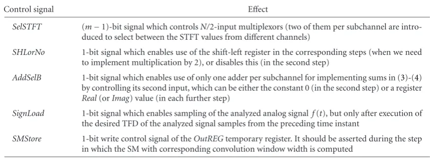
Figure1: MCI architecture for the signal-independent S-method realization.
be executed based on the execution in the first two steps, and so on. With each further step, one realizes the SM with the incremented width of convolution window, based on the pre-ceding steps. This improves the TFD concentration, aiming at achieving the one obtained by the WD.
Proposed hardware has been designed for a 16-bit fixed-point arithmetic. Each subchannel of the second block con-tains exactly one adder, one multiplier, and one shift left reg-ister for implementation of (3)-(4). These functional units must be shared for different inputs in different steps by adding multiplexors and/or a demultiplexor at their inputs. Real and imaginary parts of the SM value, computed in each execution step and based on (3)-(4), are saved into theReal andImagtemporary registers, respectively. In the first step, only the STFT block of the proposed two-block architec-ture is used, whereas in the remaining steps only the second block is used. This will be regulated by the set of control signals introduced on temporary registers, and multiplexors
and a demultiplexor, seeTable 1. Note that control signals SHLorNoandAddSelBassume unity values in each step of the TFD implementation, except in the second step (SPEC com-pletion step), when they assume zero values. Consequently, these signals can be replaced by one control signalSPECorSM that enables the SPEC execution (with its zero value), or ex-ecution of the TFDs with the nonzero convolution window widths. Note that the multiplication operation results in a two sign-bit and, assuming Q15 format (15 fractional bit), the product must be shifted left by one bit to obtain correct results. This shifter is included in the multiplier.
The longest path in the second block is one that con-nects the inputs STFTRe(n,k) (or STFTIm(n,k)), through one
Table1: Function of each of the control signal generated by the control logic.
Control signal Effect
SelSTFT (m−1)-bit signal which controlsN/2-input multiplexors (two of them per subchannel are intro-duced to select between the STFT values from different channels)
SHLorNo 1-bit signal which enables use of the shift-left register in the corresponding steps (when we need to implement multiplication by 2), or disables this (in the second step)
AddSelB 1-bit signal which enables use of only one adder per subchannel for implementing sums in (3)-(4) by controlling its second input, which can be either the constant 0 (in the second step) or a register
Real(orImag) value (in each further step)
SignLoad 1-bit signal which enables sampling of the analyzed analog signalf(t), but only after execution of the desired TFD of the analyzed signal samples from the preceding time instant
SMStore 1-bit write control signal of theOutREGtemporary register. It should be asserted during the step in which the SM with corresponding convolution window width is computed
an application specified integral circuits (ASIC) chip to meet the speed and performance demands of very fast real-time applications, seeSection 4.
Defining the control
From the defined multistep sequence of the multicycle TFDs execution, we can determine what control logic must do at each clock cycle. It can set all control signals, based solely on the distribution code (TFDcode). This code determines TFD which will be implemented by using the proposed architec-ture. TakingN=64, the TFDcode can be a 6-bit field which determines the convolution window width. An architecture with the control logic and the control signals are shown in Figure 2.
Control for the MCI architecture must specify both the signals to be set in any step and the next step in the sequence. Here we use finite-state Moore machine to specify the multi-cycle control,Figure 3. Finite-state control essentially corre-sponds to the steps of desired TFD execution; each state in the finite-state machine will take one clock cycle. This ma-chine consists of a set of states and directions on how to change states. Each state specifies a set of outputs that are asserted or deasserted when the machine is in that particular state. The labels on the arc are conditions that are tested to determine which state is the next one. When the next state is unconditional, no label is given. Note that implementation of a finite-state machine usually assumes that all outputs that are not explicitly asserted are deasserted, and the correct op-eration of the architecture often depends on the fact that a signal is deasserted. Multiplexors and demultiplexor con-trols are slightly different, since they select one of the inputs, whether they be 0 or 1. Thus, in the finite-state machine we always specify the settings of all (de)multiplexor controls that we care about.
2.2. Trade-offs and comparisons of the proposed
design with the SCI ones
SCI architecture executes desired TFD in one clock cycle. This means that no architecture resource can be used more
than once per TFD execution and that any element needed more than once must be duplicated. Then, we can easily con-clude that in the case of the considered SM block (3)-(4) implementation we have to use (2Ld+ 1) adders, 2(Ld + 1) multipliers, and 2Ld shift left registers, if we prefer an SCI approach. This can be tested by studying the SCI architec-tures represented in [16,17], as well as real-time SCI of the SM withLd=3 given inSection 4.2.
Comparison of the architectures’ resources used in the SCI and MCI designs, as well as comparison of their clock cycle times are given inTable 2. The following advantages of the MCI design, compared with the SCI ones, can be noted:
(i) required reduction of the amount of hardware, achieved by introducing the temporary registers and several multiplexors at the inputs of the functional units. The achieved hardware reduction is significant, and it increases as the convolution window width in-creases;
(ii) since temporary registers and the introduced multi-plexors are fairly small, this could yield a substantial reduction in the hardware cost, as well as in the used chip dimensions;
(iii) the clock cycle time in the MCI design is much shorter.
Finally, the ability to realize almost all commonly used TFDs by the same hardware represents a major advantage of the proposed MCI design.
On the other hand, the fastest sampling rate in the MCI design of the SM with arbitraryLdis (Ld+2)×(Tm+2Ta+Ts), seeTable 2, while it is equal to the clock cycle time in the cor-responding SCI design (2Tm+ (Ld+ 3)Ta+Ts, seeTable 2). Then, the SCI approach improves execution time. However, this disadvantage of the MCI approach is significantly allevi-ated by the fact that the SM with smallLd is usually used,1
when the execution times in these two cases (the SCI and the MCI approaches) do not differ significantly.
1High TFD concentration (almost as high as in the WD case) is achieved
0 1 2 . . . N
2 −1
M u x
0 1 2 . . . N
2 −1
M u x
0 1 2 . . . N
2 −1
M u x
0 1 2 . . . N
2 −1
M u x
f(t) Signal A/D
16 STFT block
f(n) STFT(n, k)
Clock
SignLoad
TFD code
Control logic
SMStore SPECorSM SelSTFT
STFTRe(n, k)
STFTRe(n, k+ 1)
STFTRe(n, k+ 2)
STFTRe(n, k+N2−1)
STFTRe(n, k)
STFTRe(n, k−1)
STFTRe(n, k−2)
STFTRe(n, k−N2 + 1)
STFTIm(n, k)
STFTIm(n, k+ 1)
STFTIm(n, k+ 2)
STFTIm(n, k+N2 −1)
STFTIm(n, k)
STFTIm(n, k−1)
STFTIm(n, k−2)
STFTIm(n, k−N2 + 1)
MULT
MULT D m u x 0
1
D m u x 0
1 SHL1
SHL1 0 0
M u x 0
1
M u x 0
1 M
u x 0
1
M u x 0
1 +
+ Real
Imag CLK
CLK +
OutREG
TFD(n, k)
Figure2: MCI architecture for the signal-independent S-method realization together with the necessary control lines. Thick solid line
highlights the control line as opposed to a line that carries data.
More technical details about practical implementation of the MCI and the SCI architectures can be found inSection 4.
Hybrid implementation
In order to achieve a balance between minimal chip dimen-sions, hardware consumption and cost from the MCI ap-proach and minimal execution time from the SCI apap-proach, the hybrid implementation approach may be considered. The SM block of this implementation would be based on the SCI design of the SM with exactly defined convolution window widthLd(Ld≥1). As in the MCI design case, hybrid imple-mentation would give the desired TFD in a few clock cycles: in the second one this architecture could implement the SMs with convolution window widths up to theLd(up to the SM that is a base for the SM block realization) and in each further
step it could realize the SM with the incremental convolution window width. Then, total number of clock cycles would not be greater than the one from the MCI design. In particular, both implementation approaches, hybrid and MCI, use the same number (two) of clock cycles for the SPEC implemen-tation only. In the case of the SM with nonzero convolution window width implementation, total number of clock cycles would be smaller by using hybrid implementation design.
SignLoad=1 SMStore=0
SignLoad=0 SelSTFT=010
SPECorSM=0 (SMStore=1)
SignLoad=0 SelSTFT=110
SPECorSM=1 (SMStore=1)
SignLoad=0 SelSTFT=210
SPECorSM=1 (SMStore=1)
SignLoad=0 SelSTFT=(N2 −1)10
SPECorSM=1 (SMStore=1) Start
0
1
2
3
N
2+ 2
(TFD code=‘SPEC’)
(TFD code=‘SM withLd=1’)
(TFD code=‘SM withLd=2’)
(TFD code=‘WD’) .
. .
Figure3: The finite-state machine control for the architecture shown inFigure 2. Output (SMStore=1) means that theSMStorecontrol
signal is asserted during only the final step of the corresponding TFD execution.
implementation, since it would only slightly improve the ex-ecution time from MCI architecture (it requires only one step—SPEC completion—less than the MCI approach). The SM with Ld=2 would be a reasonable choice for this pur-pose. However, the hybrid approach would not use the whole SM block in each step. For example, part of the SM block for SPEC implementation (see Figure 12fromSection 4.2) would be used in the second step only. Note that the clock cy-cle time is determined by the longest possible path in the SM block, which does not have to be used in any step here. Con-sequently, hybrid architecture could not succeed to balance the amount of work done in each clock cycle, so that we could not minimize the clock cycle time.
Table2: Total number of functional units per channel in an SM block and the clock cycle time in the cases of (a) single-cycle implementation
(SCI) and (b) the multicycle implementation (MCI).Tmis the multiplication time of a two-input 16-bit multiplier,Tais the addition time
of a two-input 16-bit adder, whereasTsis the time for 1-bit shift. The recursive form of the STFT block implementation is assumed when
the clock cycle time in the SCI case is represented.
Implementation Adders Multipliers Shift left registers Clock cycle time
SCI 2Ld+ 1 2(Ld+ 1) 2Ld 2Tm+ (Ld+ 3)Ta+Ts
MCI 3 2 2 Tm+ 2Ta+Ts
2.3. Signal-dependent S-method
Disadvantages of the signal-independent convolution win-dow in the analysis of multicomponent signals, having dif-ferent widths of the auto-terms, motivates the introduction of a signal-dependent convolution window width. It follows, for each point of TF plane, the widths of the auto-terms excluding the summation in (1) where one or both of the components STFT(n,k +i) and STFT(n,k −i) are equal to zero. In addition, it should stop the summation outside a component. Practically, it means that when the absolute square value of STFT(n,k+i) or STFT(n,k−i) is smaller than an assumed reference level Rn, the summation in (1) should be stopped. In practice, reference value is selected based on a simple analysis of the analyzed signal and the implementation system [10,17]. It is defined as a few percent of the SPEC’s maximal value at a considered time-instantn, R2
n=maxk{SPEC(n,k)}/Q2, where SPEC(n,k) is the SPEC of analyzed signal and 1≤Q <∞. In the sequel, the signals that determine nonzero values of STFT(n,k±i) (i=0, 1,. . ., Ld(n,k)) will be denoted byx±i:x±i=1 if|STFT(n,k±i)|2> R2
n, andx±i=0 otherwise.
Sampling rate of the analyzed analog signalf(t) depends on the clock cycle time Tc and on the number of the exe-cuted steps. Consequently, the same number of steps in dif-ferent time instants must be executed. In that sense, we have to assume maximal possible convolution window width as 2Ldmax + 1 (variable convolution window width approach
with the predefined maximal window width), and to define sampling rate by (2Ldmax+ 1)Tc. Since the SM(n,k) value is
calculated in theLth step, whereL ≤Ldmax+ 1, it must be
saved up to the (Ldmax+ 1)th step into theOutREG
tempo-rary register.
In order to accommodate hardware from Figures1and 2 for signal-dependent window width, we add two N/2-input multiplexors to generateSignDep(endent) control sig-nal, which determines whether or not the ith term enters the summation in (3)-(4). With the zero value of the Sign-Dep control signal, adding the new term to the calculated SM value is disabled, since the additional improvement of the TFD concentration is impossible. It takes different values in different steps defined as
SignDep=xi·x−i, i=0, 1, 2,. . .,Ldmax. (5)
Signalsxiare set in the first step after the STFT calculation. The circuit needed to generate signalxi is separated within the dashed box and presented inFigure 4.
Multistep sequence of the signal-dependent SM is the same as in the signal-independent case. Two first steps have to be executed, since SPEC value should be forwarded to the output anyway. Namely, even if|STFT(n,k)|2 ≤ R2
n, for all k, that isx0=0, (practically, these are points (n,k) with no
signal) the convolution window width takes zero value, and then the SM takes its marginal form—SPEC [4,9]. Execu-tion of the second step is provided by setting the unit value instead ofx0to the first respective inputs of theN/2-input
multiplexors, soSignDep≡1 in the second—SPEC comple-tion step.
Defining the control
Control logic for the MCI realization of the signal-dependent SM can set all but one of the control signals, based solely on the SM enable code (SM en). Write control signal of the OutREGtemporary register is the exception. To generate it, we will need to AND together anSMStoreCondsignal from the control unit, withSignDepcontrol signal. The finite-state Moore machine that specifies the multicycle control is pre-sented inFigure 5.
3. MULTICYCLE HARDWARE IMPLEMENTATION
OF THE HIGHER-ORDER TFDS
Since the LWD is defined in the same manner as the SM (see the LWD definition (2) and the SM definition (1)), it may be realized by using the same hardware presented in Figures1 and2. For that purpose, the SM block of the proposed ar-chitecture and the second input of the output adder in the SM block must be shared (by introducing two-input mul-tiplexors) for realization of the LWD with L=2, Figure 6. This must be done since only one subchannel of the SM block is used when the SM block realizes the LWD, [25]. Namely, in that case the SM block always processes the real function SM(n,k). The function of the proposed hardware is determined by theSMorLWDcontrol signal: the SM imple-mentation and the LWD impleimple-mentation are determined by theSMorLWDzero and unit value, respectively, seeFigure 7. Note that theOutREGtemporary register is used for saving the computed SM value when we need to use the SM block for the LWD implementation.
0 1 2 . . . N
2 −1
M u x
1
x1 x2
xN 2−1
SignLoad SM en
SMStoreCond SPECorSM SelSTFT
SignDep Control
logic
SignDep
0 1 2 . . . N
2 −1
M u x
1
x−1 x−2
x−N 2+1
STFTRe(n, k)
STFTIm(n, k) f(t)
Signal A/D
16 STFT block
f(n) STFT(n, k)
Clock
0 1 2 . . . N
2−1
M u x
0 1 2 . . . N
2−1
M u x
0 1 2 . . . N
2−1
M u x
0 1 2 . . . N
2−1
M u x STFTRe(n, k+ 1)
STFTRe(n, k+ 2)
STFTRe(n, k+N2 −1)
STFTRe(n, k−1)
STFTRe(n, k−2)
STFTRe(n, k−N2 + 1)
STFTIm(n, k+ 1)
STFTIm(n, k+ 2)
STFTIm(n, k+N2−1)
STFTIm(n, k−1)
STFTIm(n, k−2)
STFTIm(n, k−N2+1)
MULT MULT
D m u x 0
1
D m u x 0
1 SHL1
SHL1 0
0 M u x 0
1
M u x 0
1 M u x 0
1
M u x 0
1 +
+ Real
Imag CLK
CLK +
OutREG
TFD(n, k)
STFTRe(n, k+i)
STFTIm(n, k+i)
MULT
MULT +
R2
Comp xi
Figure4: MCI architecture for the signal-dependent S-method realization.
SignLoad=1 SMStoreCond=0
SignLoad=0 SelSTFT=010
SPECorSM=0 SMStoreCond=1
SignLoad=0 SelSTFT=110
SPECorSM=1 SMStoreCond=1
SignLoad=0 SelSTFT=210
SPECorSM=1 SMStoreCond=1
SignLoad=0 SelSTFT=(Ldmax)10
SPECorSM=1 SMStoreCond=1 Start
0 1 2 3
Ldmax+ 1
1
0 M u x SignLoad
TFD code
SMStore Add SelB SHLorNo SelSTFT Control
logic
SMorLWD
STFTRe(n, k)
STFTIm(n, k) f(t)
Signal A/D
16 STFT block
f(n) STFT(n, k)
CLK
0 1 2 . . . N
2 −1
M u x
0 1 2 . . . N
2 −1
M u x
0 1 2 . . . N
2 −1
M u x
0 1 2 . . . N
2 −1
M u x STFTRe(n, k)
STFTRe(n, k+ 1)
STFTRe(n, k+ 2)
STFTRe(n, k+N2 −1)
STFTRe(n, k−1)
STFTRe(n, k−2)
STFTRe(n, k−N2 + 1)
STFTIm(n, k)
STFTIm(n, k+ 1)
STFTIm(n, k+ 2)
STFTIm(n, k+N2 −1)
STFTIm(n, k−1)
STFTIm(n, k−2)
STFTIm(n, k−N2 + 1)
MULT
MULT D m u x 0
1
D m u x 0
1 SHL1
SHL1 0
0 M
u x 0
1
M u x 0
1 M u x 0
1
M u x 0
1 +
+ Real
Imag CLK
CLK +
OutREG
TFD(n, k)
SMorLWD
1
0 M u
x 0
Figure6: A complete hardware for one channel simultaneous realization of the S-method/L-Wigner distribution.
signal. The finite-state machine control for this system is shown inFigure 7. If we repeat the last Ld + 1 steps from Figure 7(i.e., stepsLd+ 2 to 2Ld+ 2), together with assert-ing of theSMStorecontrol signal in the (2Ld+ 2)th step, the LWD withL=4 is implemented by using the proposed ar-chitecture.
Here we do not analyze the finite register length influence on the accuracy of the results obtained by the proposed archi-tecture. Its rigorous treatment may be found in [26]. Also, for the numerical illustration we refer the readers to the papers where the theoretical approach for the methods used in this paper is given, [4,9,10,12,16].
4. PRACTICAL IMPLEMENTATION APPROACH
The architectures for the SM calculation from the STFT sam-ples can be practically realized by using different technologies
SignLoad=1 SMStore=0
SMorLWD=1 SignLoad=0 SelSTFT=010 SHLorNo=0 Add SelB=1 SMStore=1
SMorLWD=1 SignLoad=0 SelSTFT=110 SHLorNo=1 Add SelB=1 SMStore=0
SMorLWD=1 SignLoad=0 SelSTFT=210 SHLorNo=1 Add SelB=1 SMStore=0
SMorLWD=1 SignLoad=0 SelSTFT=(Ld)10
SHLorNo=1 Add SelB=0 SMStore=0
SMorLWD=0 SignLoad=0 SelSTFT=010 SHLorNo=0 Add SelB=0 (SMStore=1)
SMorLWD=0 SignLoad=0 SelSTFT=110 SHLorNo=1 Add SelB=1 (SMStore=1)
SMorLWD=0 SignLoad=0 SelSTFT=210 SHLorNo=1 Add SelB=1 (SMStore=1)
SMorLWD=0 SignLoad=0 SelSTFT=(Ld)10
SHLorNo=1 Add SelB=1 SMStore=1 Start 0
1
2
3
Ld+ 1 2Ld+ 2
2Ld+ 1
2Ld
Ld+ 2
(TFD code=‘LWD withL=2 andLd=1’)
(TFD code=‘LWD withL=2 andLd=2’)
(TFD code=‘LWD withL=2 andLd’)
(TFD code=‘SPEC’)
(TFD code=‘SM withLd=1’)
(TFD code=‘SM withLd=2’)
(TFD code=‘SM withLd’) .
. .
. . .
Figure7: The finite-state machine control for the multicycle hardware implementation fromFigure 6.
blocks and memory areas. These can be used to built power-ful specialized parallel processing units such as adders, mul-tipliers, shifters, and so forth in form of schematic entry or the VHDL code. The internal memory blocks (RAMs, ROMs and FIFOs, etc.) are usable for fast interconnection between parallel structures, as well as to generate the control signals and to configure the system.
In this section, both MCI and SCI architectures are implemented in the FPGA chips. The MCI architecture
From STFT module
0
Ld
2Ld
. . .
. . .
. . . STFT(n, k+Ld) STFT(n, k+Ld−1)
STFT(n, k)
STFT(n, k−Ld+ 1) STFT(n, k−Ld)
MUX1
SelSTFT 1
MUX2
SelSTFT 2
×
MULT
ShLEFT
SHLorNo
CumADD
OutREG
SM(k) +
1-bits
Shift memory buffer (ShMemBuff)
Configuration signals (from PC or MC)
SMStore/STFTLoad RESET
Control logic
Bin counter
TFD code
System clock
LUT (RAM
or ROM) LUT Add
SelSTFT 1 SelSTFT 2 CLK RESET
SHLorNo
SMStore/STFTLoad CLK1
RESET (ADD clear) SMStore/STFTLoad
Figure8: Block diagram of FPGA implementation of the MCI approach.
(EAB), and so on. The computation units are realized by using standard digital components in form of schematics entries or by Altera hardware design language (AHDL)-based mega-functions (library of parametrized modules (LPM)).
The proposed MCI and SCI architectures, implemented in FPGA technology, will be shortly described and com-pared against usual criteria such as chip capacity, computa-tion speed, power consumpcomputa-tion, and cost.
4.1. Implementation of the MCI architecture
The FPGA-based implementation of the MCI architecture follows the design logic given inFigure 8. Since the real and imaginary computation lines are identical, the interpreta-tion will be done through real ones. As seen, it consists of several functional blocks (units). The STFT sample is im-ported from the STFT module to the Shift Memory Buffer (ShMemBuff) that is implemented as an array of parallel-in-parallel-out registers. Their outputs represent the STFT samples in time order STFT(n,k+Ld), STFT(n,k+Ld − 1),. . ., STFT(n,k),. . ., STFT(n,k−Ld+ 1), STFT(n,k−Ld) and due to each SMStore/STFTLoad cycle, they have been shifted for one position. These are also fed to the inputs of multiplexors MUX1 and MUX2 and, two-by-two, regarding on multiplexor’s addresses SelSTFT 1 and SelSTFT 2, for-warded to the parallel multiplier MULT in order to produce
partial product term according to (3). This term is either shifted left or not, depending on the signalSHLorNo. This shift is performed by shifterShLEFT, the output of which is connected to the first input of the cumulative pipelined adderCumADD. TheCumADDhas been designed to replace an adder and a multiplexor (addressed by theAddSelB con-trol signal) from Figures1and2. The time diagram of calcu-lation process is presented inFigure 9. As shown, the multi-plying and shifting operations are parallel, while the adding has a latency of one clock. AfterLd + 1 clocks, the output of theCumADD will contain the sum SM(n,k) that repre-sents the final value of the SM. The next two cycles are used for the signalsSMStore/STFTLoadand RESET that will store the sum SM(n,k) in the output register and resetCumADD to zero, respectively. Use of the RESET signal will increase the calculation time for one clock. It means that the calcula-tion process takesLd+ 3 cycles, one more than is elaborated inFigure 3. Note that the RESET signal can be generated by the signalSMStore/STFTLoad, using a short delay, that will reduce the calculation process to Ld+ 2 cycles. In order to clarify the principle of calculation and simulation (the pro-cess of cumulative sums cumSM represented inFigure 11), we have used the first variant of RESET generation, with Ld+ 3 clocks.
System clock CLK
SMStore/STFTLoad
RESET
SHLorNo
1 2 Ld+ 1
StoreSM(n, k−1)/LoadSTFT(n, k+Ld) SelSTFT 1(n, k)/SelSTFT 2(n, k)
0+STFT(n, k)∗STFT(n, k)=Sum(0) SelSTFT 1(n, k+ 1)/SelSTFT 2(n, k−1)
Sum(0) + 2∗(STFT(n, k+ 1)∗STFT(n, k−1)=Sum(1) SelSTFT 1(n, k+Ld)/SelSTFT 2(n, k−Ld)
Sum(Ld−1) + 2∗(STFT(n, k+Ld)∗STFT(n, k−Ld))=SM(n, k) StoreSM(n, k)/Load STFT(n, k+Ld+ 1)
Figure9: The calculation-timing diagram for block diagram fromFigure 8.
Table3: LUT’s values for givenLd. The ADD(STFT(n,k)) means the address location of the STFT(n,k) sample inside ShMemBuff, whereas
m=CEIL(log2N)=Length(SelSTFT 1). Symbol “” denotes logical shift left operation. Note that signalsSHLorNo, RESET and
SM-Store/STFTLoadmake control signals area.
LUT’s memory location SHLorNo RESET SMStore/STFTLoad SelSTFT 1bits SelSTFT 2bits
0 0 0 0 ADD(STFT(n,k))m ADD(STFT(n,k))
1 1 0 0 ADD(STFT(n,k+ 1))m ADD(STFT(n,k−1))
— 1 0 0 — —
Ld 1 0 0 ADD(STFT(n,k+Ld))m ADD(STFT(n,k−Ld))
Ld+ 1 0 0 1 0 0
Ld+ 2 0 1 0 0 0
signals area (which consists of signalsSHLorNo, RESET, and SMStore/STFTLoad, resp.) and MUXs’ addresses. The binary counter (see Figure 8) generates the low LUT’s addresses, while TFDcode register sets the high ones. It means that starting address of the running memory block is assigned to the corresponding value Ld stored in TFDcoderegister. At the end of the sequence, the binary counter is cleared by the signal RESET. During system initialization, the mem-ory contents and value of TFDcode register are automati-cally loaded from outside by using PC or general-purpose microcontroller. Of course, these parameters can be perma-nently stored using ROMs, EEPROMs, and FLASHs instead of RAMs.
Figure 10shows a schematic diagram for SM calculation from the STFT samples (STFT to SM gateway) using MCI approach. The control logic is realized by using ROM. The maximal register widths for each unit determine the capacity of the assigned chip. The critical point is the width of the CumADD. It is a function of both STFT data length and the maximal possible convolution window widthLdmaxthat
can be implemented by using proposed architecture.Table 4 shows the relations between minimum widths of units and parametersl(data length) andLdmax. In order to verify the
STFT( n, k + Ld ) (M ultiple xers) (M ultiplier) (Shift re gi st er) (C um ulati ve adder) Mu x1 MUL T ShLEFT Cu m A D D LPM MUX LPM MUL T LPM CLSHIFT LPM ADD SUB Input STFT[7 .. 0][7 .. 0] data[][] STFT[0][7 .. 0] STFT[7 .. 0][7 .. 0] data[][] Re su lt [] Re su lt [] Output sel[] sel[] SelSTFT[5 .. 3] SelSTFT[2 .. 0] Cu m S M [1 9 .. 0] STFT[0][7 .. 0] 8bit re g D[7 .. 0] Q[7 .. 0] CLK STFT[1][7 .. 0] 8bit re g D[7 .. 0] Q[7 .. 0] CLK STFT[2][7 .. 0] 8bit re g D[7 .. 0] Q[7 .. 0] CLK STFT[3][7 .. 0] 8bit re g D[7 .. 0] Q[7 .. 0] CLK STFT[4][7 .. 0] 8bit re g D[7 .. 0] Q[7 .. 0] CLK STFT[5][7 .. 0] 8bit re g D[7 .. 0] Q[7 .. 0] CLK STFT[6][7 .. 0] 8bit re g D[7 .. 0] Q[7 .. 0] CLK STFT[7][7 .. 0] SelSTFT[6] (Shift memor y bu ff er) ShM emB u ff MUX2 LPM MUX C o nt ro l L og ic SelSTFT[7] 7493 RO 1 RO 2 CLK A CLKB
QA QB QC QD
C
o
unt
er
A
dd[0] Add[1] Add[2] Add[3]
CLK INPUT NO T CLK1 A dd[3..0] LPM RO M A ddr ess[] q[] RO M SelSTFT[7] Soft SelSTFT[6] Soft SelSTFT[8 .. 0] SelSTFT[8] Soft
Output Output Output Output
Re se t St or eSM/L o ad STFT SelSTFT[8 .. 0] ShL o rN o[0] ShL o rN o[0] ShL o rN o[1] ShL o rN o[2] ShL o rN o[3] ShL o rN o[4] GND G ND GND G ND Dataa[] Datab[] Re su lt [] c[ 1 5 .. 0] c[17 .. 0] c[17 .. 16] GND ShLorN o[4 .. 0] GND Data[] Distanc e[] Dir ectio n Re su lt [] Un d er fl o w Ov er flo w a[17 .. 0] a[19 .. 0] a[19 .. 18] GND CLK1 Ci n
Dataa[] Clock Datab[] Ac
Table4: Output register lengths for used digital units depending on the parametersl,Ldmax.
Length of MUX1, MUX2 MULT ShLEFT CumADDandOutREG
Parametersl,Ldmax l 2·l 2·l+ 1 CEIL(log2((22l+1−1)·(Ldmax+ 1)))
Ref: 0 ns Time: 2.32 us Interval: 2.32 us
Name: Value: 5 us 10 us 15 us 20 us
CLK
SM/Load STFT RESET SelSTFT[8..0] ShLorNo[0] STFT0 [7..0] cumSM[19..0] SM[19..0]
0 0 0 D 18
D 0 D 5 D 0 D 0
18 267 260 64 18 267 260 64 18 267 260 64
0 1 1 0 0 1 1 0 0 1 1 0
5 6 7
0 0 0 25
0 (a)
Ref: 0 ns Time: 26.36 us Interval: 26.36 us
Name: Value: 25 us 30 us 35 us 40 us 45 us
CLK SM/Load STFT
RESET SelSTFT[8..0] ShLorNo[0] STFT0 [7..0] cumSM[19..0] SM[19..0]
0 0 0 D 18
D 0 D 5 D 0 D 0
64 18 267 260 64 18 267 260 64 18 267 260
0 0 1 1 0 0 1 1 0 0 1 1
7 8 9 0
25 0 36 106 0 49 145 235 0 64 190
25 106 235
(b)
Figure11: Simulation illustration for test vectorV={5, 6, 7, 8, 9, 0, 0,. . .}andLd=3.
4.2. Implementation of the SCI architecture
As opposite to the MCI architecture, the SCI has no latency [17]. The arithmetic units are realized by using combina-tional logic, meaning that all calculation operations are per-formed in parallel. The schematic diagram of its FPGA im-plementation is given inFigure 12. As seen, there is no need for input multiplexors and control signals such asSMStore/ STFTLoad, SelSTFT 1, SelSTFT 2, RESET and SHLorNo. Thus, the ROM based generator is needless. At the rising edge of the system clock CLK, the STFT samples are shifted, and due to falling edge, the final result is stored in output registerOutREG, as shown in the simulation diagram given in Figure 13. One parallel multiplier and one shift register are used for each of product terms from (3), expect for the SPEC term that has no shift register. These terms are added by using cascade network of two-inputs parallel adders,
giving the final sum SM[19· · ·0]. The register widths are the same as in the case of MCI. It should be emphasized that the number of multipliers, shift register, and adders drastically increases with the order ofLd. For example, for Ld=3 we need 4 multipliers (MULT1· · ·4), 3 shift registers (ShLEFT1· · ·3), and 3 adders (ParADD1· · ·3),Figure 12.
4.3. Comparison of MCI and SCI architectures
Ref: 9 ns Time: 0 us Interval: −9 us
Name: Value: 2 us 4 us 6 us 8 us 10 us 12 us 14 us 16 us
9 us CLK
STFT0 [7..0] SM[19..0]
1 D 9 D 25
5 6 7 8 9 0
0 25 106 235 190
Figure13: Simulation diagrams for SCI architecture. The overall computation process is performed in one clock cycle.
Table5: Summarized implementation utilization for real devices andLd=3 andN=8 and data lengthsl=8 andl=16.
Computation architecture Total logic
cells (LCs) used
Total flip-flops used
Memory bits used
Total I/O pins used
Utilized LCs for recom-mended device
Recommended device
Real 8-bits MCI 641 101 144 41 55% EPF10K20TC144-3
Real 8-bits SCI 1728 75 0 29 100% EPF10K30RC208-3
Real 16-bits MCI 1772 197 144 69 76% EPF10K40RC208-3
Real 16-bits SCI 5498 147 0 57 No fit Not fit in the largest of 10 K
EPF10K100GC503-3DX4992
66% EP20K200
Real + Imag 8-bits MCI 1281 198 144 69 74% EPF10K30RC208-3
Real + Imag 8-bits SCI 3532 150 0 57 94% EPF10K70RC240-2
Real + Imag 16-bits MCI 3543 397 144 125 94% EPF10K70RC248-3
Real + Imag 16-bits SCI 11237 294 0 113 No fit Not fit in the largest of 10 K
EPF10K100GC503-3DX4992
67% EP20K400
devices (total logic cells (LCs)) as a function ofLd, for con-stantN=16, and data lengthl=8 is illustrated inFigure 14.
As seen, the main advantages of MCI architecture are as follows:
(i) for the same Ld, the MCI architecture needs signifi-cantly less LCs for its implementation. It is known that the capacity of chip, that is, the silicon area, is directly proportional to the number of allowed LCs. Since the MCI architecture is structurally identical for different Lds, the number of LCs could only slightly increase with the increase of N. That is caused by the input span and address lengths of multiplexors (MUX1 and MUX2 fromFigure 10);
(ii) the reduced power consumption, which is strongly proportional to the chip capacity; and
(iii) less implementation cost (about 2-3 times).
An advantage of the SCI architecture is the processing speed that is of importance for time-critical applications. The number of LCs significantly varies byLd(about 400–500 LCs perLd) that complicates the design and increases the imple-mentation cost and power consumption.
After the simulation, the real FLEX 10 K devices are configured at system power-up using Atlera’s UP2 develop-ment board with data from ByteBlasterMV. Microcontroller emulated the STFT front end, while the calculated SM was collected and verified by a PC. Because reconfiguration re-quires less than 320 ms (in case of using external configura-tion EEPROM), real-time changes can be made during sys-tem operation.
5. CONCLUSION
0 500 1000 1500 2000 2500
2 3 4 Ld 5
MCI SCI Total LCs used
Figure14: The dependance of the LCs used assumingN=16, and
data lengthl=8.
its implementations in FPGA devices and compared with the SCI architecture against usual criteria such as chip capacity, computation speed, power consumption, and cost.
REFERENCES
[1] L. Cohen, “Time-frequency distributions—a review,”
Proceed-ings of the IEEE, vol. 77, no. 7, pp. 941–981, 1989.
[2] F. Hlawatsch and G. F. Boudreaux-Bartels, “Linear and
quadratic time-frequency signal representations,”IEEE Signal
Processing Magazine, vol. 9, no. 2, pp. 21–67, 1992.
[3] L. Cohen, “Preface to the special issue on time-frequency
anal-ysis,”Proceedings of the IEEE, vol. 84, no. 9, pp. 1197–1197,
1996.
[4] LJ. Stankovi´c, “A method for time-frequency analysis,”IEEE
Transactions on Signal Processing, vol. 42, no. 1, pp. 225–229, 1994.
[5] B. Boashash and B. Ristic, “Polynomial time-frequency distri-butions and time-varying higher order spectra: application to the analysis of multicomponent FM signals and to the
treat-ment of multiplicative noise,”Signal Processing, vol. 67, no. 1,
pp. 1–23, 1998.
[6] P. Goncalves and R. G. Baraniuk, “Pseudo affine Wigner
distri-butions: definition and kernel formulation,”IEEE Transactions
on Signal Processing, vol. 46, no. 6, pp. 1505–1516, 1998. [7] C. Richard, “Time-frequency-based detection using
discrete-time discrete-frequency Wigner distributions,”IEEE
Transac-tions on Signal Processing, vol. 50, no. 9, pp. 2170–2176, 2002. [8] L. L. Scharf and B. Friedlander, “Toeplitz and Hankel
ker-nels for estimating time-varying spectra of discrete-time
ran-dom processes,”IEEE Transactions on Signal Processing, vol. 49,
no. 1, pp. 179–189, 2001.
[9] LJ. Stankovi´c, V. N. Ivanovi´c, and Z. Petrovi´c, “Unified ap-proach to the noise analysis in the spectrogram and Wigner
distribution,”Annales des Telecommunications, vol. 51, no.
11-12, pp. 585–594, 1996.
[10] S. Stankovi´c and LJ. Stankovi´c, “An architecture for the
real-ization of a system for time-frequency signal analysis,”IEEE
Transactions on Circuits And Systems—Part II: Analog and Dig-ital Signal Processing, vol. 44, no. 7, pp. 600–604, 1997. [11] LJ. Stankovi´c and J. F. B¨ohme, “Time-frequency analysis of
multiple resonances in combustion engine signals,”Signal
Pro-cessing, vol. 79, no. 1, pp. 15–28, 1999.
[12] LJ. Stankovi´c, “A method for improved distribution concen-tration in the time-frequency analysis of multicomponent
sig-nals using the L-Wigner distribution,”IEEE Signal Processing
Magazine, vol. 43, no. 5, pp. 1262–1268, 1995.
[13] K. J. R. Liu, “Novel parallel architectures for short-time
Fourier transform,” IEEE Transactions on Circuits And
Systems—Part II: Analog and Digital Signal Processing, vol. 40, no. 12, pp. 786–790, 1993.
[14] M. G. Amin and K. D. Feng, “Short-time Fourier transforms
using cascade filter structures,”IEEE Transactions on Circuits
And Systems—Part II: Analog and Digital Signal Processing, vol. 42, no. 10, pp. 631–641, 1995.
[15] B. Boashash and P. Black, “An efficient real-time
implemen-tation of the Wigner-Ville distribution,”IEEE Transactions on
Acoustics, Speech, and Signal Processing, vol. 35, no. 11, pp. 1611–1618, 1987.
[16] D. Petranovi´c, S. Stankovi´c, and LJ. Stankovi´c, “Special
pur-pose hardware for time-frequency analysis,”Electronics Letters,
vol. 33, no. 6, pp. 464–466, 1997.
[17] S. Stankovi´c, LJ. Stankovi´c, V. N. Ivanovi´c, and R. Stojanovi´c, “An architecture for the VLSI design of systems for
time-frequency analysis and time-varying filtering,” Annales des
Telecommunications, vol. 57, no. 9-10, pp. 974–995, 2002. [18] K. Maharatna, A. S. Dhar, and S. Banerjee, “A VLSI array
ar-chitecture for realization of DFT, DHT, DCT and DST,”Signal
Processing, vol. 81, no. 9, pp. 1813–1822, 2001.
[19] K. J. R. Liu and C.-T. Chiu, “Unified parallel lattice structures for time-recursive discrete cosine/sine/Hartley transforms,” IEEE Transactions on Signal Processing, vol. 41, no. 3, pp. 1357– 1377, 1993.
[20] A. Papoulis, Signal Analysis, McGraw-Hill, New York, NY,
USA, 1977.
[21] A. V. Oppenheim and R. W. Schafer,Digital Signal Processing,
Prentice-Hall, Englewood Cliffs, NJ, USA, 1975.
[22] M. G. Amin, “A new approach to recursive Fourier transform,” Proceedings of the IEEE, vol. 75, no. 11, pp. 1537–1538, 1987.
[23] M. Unser, “Recursion in short-time signal analysis,” Signal
Processing, vol. 5, no. 3, pp. 229–240, 1983.
[24] M. G. Amin, “Spectral smoothing and recursion based on the
nonstationarity of the autocorrelation function,”IEEE
Trans-actions on Signal Processing, vol. 39, no. 1, pp. 183–185, 1991. [25] V. N. Ivanovi´c and LJ. Stankovi´c, “Multiple clock cycle
real-time implementation of a system for real-time-frequency analysis,” inProceedings of 12th European Signal Processing Conference (EUSIPCO ’04), pp. 1633–1636, Vienna, Austria, September 2004.
[26] V. N. Ivanovi´c, LJ. Stankovi´c, and D. Petranovi´c, “Finite word-length effects in implementation of distributions for
time-frequency signal analysis,”IEEE Transactions on Signal
Veselin N. Ivanovi´c was born in Cetinje, Montenegro, April 10, 1970. He received the B.S. degree in electrical engineering (1993) and the M.S. degree in electrical engineering from the University of Mon-tenegro (1996). He received the Ph.D. de-gree in electrical engineering from the same University (2001) in time-frequency signal analysis and architecture design for imple-mentation of time-frequency methods and
time-varying filtering. In 2001, he received the Siemens Award for scientific achievements in his Ph.D. research. Dr. Ivanovi´c is an Assistant Professor (Docent) at the Electrical Engineering Depart-ment, University of Montenegro. He is also Vice-Dean at the elec-trical engineering Department, University of Montenegro. His re-search interests are in the areas of time-frequency signal analysis, hardware/software codesign, computer organization and design, and design with microcontrollers.
Radovan Stojanovi´cwas born in Berane, Montenegro, Yugoslavia, November 18, 1965. He received the B.S.E.E. and M.S.E.E. degrees from the University of Montenegro, and the Ph.D. degree from the University of Patras, Greece, in 1991, 1994, and 2001, re-spectively. From 1990 to 1998, he was at the Electrical Engineering Department, Univer-sity of Montenegro. From 1998 to 2001, he was a Research Associate at the Department
of Electrical Engineering and Computer Technology, University of Patras, Greece. After that, he spent two years as a Senior Researcher in the Industrial System Institute (ISI), Patras, Greece. Currently, he is an Assistant Professor at the University of Montenegro guid-ing the group of applied electronics. His fields of interest are hard-ware/software codesign, applied signal and image processing, and industrial and medical electronics.
LJubiˇsa Stankovi´cwas born in Montene-gro, June 1, 1960. He received the B.S. de-gree in electrical engineering from the Uni-versity of Montenegro, in 1982, with the honor “the best student at the University,” the M.S. degree in electrical engineering, in 1984, from the University of Belgrade, and the Ph.D. degree in electrical engineering in 1988 from the University of Montene-gro. As a Fulbright grantee, he spent the
1984/1985 academic year at the Worcester Polytechnic Institute, Massachusetts. Since 1982, he has been on the faculty at the Uni-versity of Montenegro, where he now holds position of a Full Pro-fessor. Stankovi´c was also active in politics, as a Vice-President of the Republic of Montenegro (1989–1991), and then the leader of democratic (anti-war) opposition in Montenegro (1991–1993). During 1997/1998 and 1999, he was on leave at the Ruhr University Bochum, Germany, with Signal Theory Group, supported by the Alexander von Humboldt foundation. At the beginning of 2001, he spent a period of time at the Technische Universiteit Eindhoven, the Netherlands, as a Visiting Professor. During the priod of 2001– 2002 he was the President of the Governing Board of the Mon-tenegrin mobile phone company “MONET.” His current interests are in signal processing and electromagnetic field theory. He pub-lished about 270 technical papers, more than 80 of them in lead-ing international journals, mainly the IEEE editions. He has pub-lished several textbooks about signal processing (in Serbo-Croat)
and the monographTime-Frequency Signal Analysis(in English).