International Journal of Emerging Technology and Advanced Engineering
Website: www.ijetae.com (ISSN 2250-2459,ISO 9001:2008 Certified Journal, Volume 3, Issue 11, November 2013)
172
Design of Multi Level Converter for Interline Power Flow
Controller with Variable Inputs in SIMULINK/MATLAB
M. Venkateswarareddy
1,Dr. Bishnu Prasad Muni
2,
Ph.D, Dr. A.V.R. S. Sarma
3,
Ph.D, 1Research Scholar(Ph.D), Electrical Engineering Dept., University college of Engineering, Osmania University, A.P India
2Additional General Manager, Bharat Heavy Electricals Limited(R&D), BALA NAGAR, Hyderabad, India
3Professor EE Dept., University College of Engg, Osmania University Hyderabad, India
Abstract--The Interline Power Flow Controller (IPFC) a concept for the compensation and effective power flow management of multi-line transmission systems. In its general form, the IPFC employs two or more number of converters (VSC) with a common dc link, each to provide series compensation for a selected line of the transmission system. Because of the common dc link, any converter within the IPFC is able to transfer real power to any other and thereby facilitate reactive power transfer among the lines of the transmission system. Since each converter is also able to provide reactive power compensation, the IPFC is able to carry out an overall real and reactive power compensation of the total transmission system. This capability makes it possible to equalize both real and reactive power flow between the lines, transfer power from overloaded to under loaded lines, compensate against reactive voltage drops and the corresponding reactive line power, and to increase the effectiveness of the compensating system against dynamic disturbances. The paper explains the basic theory and operating characteristics of the five level inverter based IPFC with phasor diagrams, and simulated waveforms in SIMULINK/MATLAB
Keywords - AC transmission, FACTS, IPFC, line
compensation, 5 level inverter, power flow controller, Series compensation, VSC.
Section I
I. INTRODUCTION
Flexible AC Transmission Systems (FACTS) based on either Voltage or Current Source converters (VSC/CSC) these can be used to control steady-state as well as dynamic/transient performance of the power system. Converter-based FACTS controllers when compared to conventional switched capacitor/reactor and thyristor -based FACTS controllers such as Static Var Compensator (SVC) and Thyristor-controlled Series Capacitor (TCSC) have the advantage of generating/absorbing reactive power without the use of ac capacitors and reactors.
In addition converter-based FACTS controllers are capable of independently controlling both active and reactive power flow in the power system. Series connected
converter-based FACTS controllers include Static
Synchronous Series Compensator (SSSC), Unified Power Flow Controller (UPFC) and Interline Power Flow Controller (IPFC). A SSSC is a series compensator with ability to operate in active/inductive modes to improve the system stability. The IPFC includes a Static Synchronous compensator (STATCOM) and a SSSC that share a common dc-link.
The IPFC consists of two or more SSSC with a common dc-link so, each SSSC contains a VSC that is in series with the transmission line through a coupling transformer, and injects a voltage with controllable magnitude and phase angle into the line. IPFCs provide independent control of reactive power of each individual line, while active power could be transferred via the dc-link between the compensated lines.
Section II
A. Inter line power flow controller
International Journal of Emerging Technology and Advanced Engineering
Website: www.ijetae.com (ISSN 2250-2459,ISO 9001:2008 Certified Journal, Volume 3, Issue 11, November 2013)
173
[image:2.612.73.237.142.256.2]
Fig.1. IPFC model
[image:2.612.64.298.314.446.2]With this scheme in addition to providing series reactive compensation, any converter Cn be controlled to supply active power to the common dc link from its own transmission line.
Fig. 1. Basic two inverter power flow controller
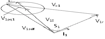
B. Operating principle and phasor diagram for interline power flow controller
For simplicity for explaining of 3 phase IPFC a single phase IPFC was taken. The IPFC(Fig. 2) is designed with a combination of the two series connected VSC which can inject a voltage with controllable magnitude and phase angle at the fundamental frequency, while DC link voltage maintained at a desired level. The common dc link is
represented by a bidirectional link (P12 =P1pq = P2pq) for
real power exchange between two voltage sources. Transmission line reactance represented by X1 has a
sending end bus with voltage Phasor V1s and a receiving
end voltage Phasor V1r. The sending end voltage Phasor of
Line2, represented by reactance X2, is V2s and the
receiving-end voltage Phasor is V2r. Simply, all the
sending-end and receiving-end voltages are assumed to be
constant with fixed amplitudes, V1s = V1r = V2s = V2r =1pu.,
and with fixed angles resulting in identical transmission
angle s1 = s2 for the two systems. The two line impedances
and the rating of the two compensating voltage sources are also assumed to be identical.
This means X1 = X2 and V1pqmax = V2pqmax. Although in
practice system1 and system2 could be likely different due to different transmission line voltage, impedance and angle. We assumed system1 is arbitrarily selected to be the prime system for which free controllability of both real and reactive line power flow is stipulated to derive the constraints the free controllability of system1 forces on the power flow control of system2. A phasor diagram of system1 illustrated in Figure 3 defines the relationship
between V1s, V1r, Vx1 (the voltage phasor across X1) and
the inserted voltage phasor V1pq, with controllable
magnitude and angle.
V1pq is added to the sending end voltage V1self = V1s +
V1pq. So V1self –V1r, the difference sets the compensated
voltage phasor or Vx1 across reactance X1. As angle is
varied over its full 360 degree range, the end of phasor V1pq
moves along a circle with its center located at the end of
phasor V1s. The area within this circle defines the operating
range of phasor V1pq. Thus the line1 can be compensated.
The rotation with angle of phasor V1pq modulates both the
magnitude and the angle of phasor Vx1 and, therefore, both
the transmitted real power, P1r, and the reactive power, Q1r,
vary with 1.
Fig.3. PHASOR Diagram Of System
This process requires the voltage source representing
Inverter 1(V1pq) to supply and absorb both reactive, (Q1pq),
and real, (P1pq) power.
Section III
II. DESIGN OF FIVE LEVEL CONVRTER
By using modern power electronics more revolution came in power generation and transmission. In the area of conversion (from AC- DC or DC to AC) the ability to continuous vary in output voltage, frequency and amplitude by selecting the right device. And their control. The high level inverters generate the ac voltages by switching at different levels at high frequency with semiconductor devices. The waveforms generated the inverter is differ from the general sinusoidal waveform because of rectangular switching.
DC common link
SSSC SSSC
V i
V i V i
[image:2.612.368.548.412.479.2]International Journal of Emerging Technology and Advanced Engineering
Website: www.ijetae.com (ISSN 2250-2459,ISO 9001:2008 Certified Journal, Volume 3, Issue 11, November 2013)
174
A.Three Phase 5 Level Inverter
The above fig shows the three phase five level inverter which consists of totally twenty four IGBTS for three legs (Each leg consists 8 IGBTS) which are protected by anti parallel diodes. These anti parallel diodes are working as snubber circuits for protecting the IGBTS. For simplicity in explaining the operation of three phase inverter single leg was taken, the construction of single leg and design of capacitor explained in next paragraphs.
One pole (or phase) of the five level inverter is shown in Fig.5. where two additional poles would be required for a three phase VSI. Each IGBT is equipped with average conducting diode and a diode clamp to ensure that the voltage across a single IGBT does not exceed the voltage cross the supply. The lower four IGBT require the complementary gating pulses of upper four IGBTS of the same number. That is if 43 is on, then 43' must be off. The gate logic to achieve the five voltage levels at the output Va is shown in Table 1.
International Journal of Emerging Technology and Advanced Engineering
Website: www.ijetae.com (ISSN 2250-2459,ISO 9001:2008 Certified Journal, Volume 3, Issue 11, November 2013)
175
B. Various Strategies for The Control Of The Output Of
Five Level Inverter
Voltage and frequency were investigated on the basis of number --of IGBT switching’s per fundamental cycle and the distortion factor defined as the rms value of the
harmonic voltages normalized to the maximum
fundamental voltage and divided by the harmonic number.
Table1.
Switching sequence for five level inverter
All odd non-triple harmonics where considered. A low distortion factor implies low losses due to harmonic voltages and currents and a low torque ripple.
Both fundamental frequency switching of the IGBTS with variable dc link voltages, and PWM techniques with fixed dc link voltages were studied.
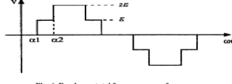
C. Fundamental Frequency Switching
Fundamental frequency switching requires each device to be switched on and off just once per cycle of the fundamental frequency output and produces the staircase type waveform of Fig.6 There are a number of degrees of
freedom that can be employed in arriving fundamental
frequency switching at an optimum type of output voltage
waveform. If we switch to the intermediate voltage, +E at αl, and to the full voltage, +2E at α2, the Fourier coefficients of the output voltage are calculated as the simple sum of the coefficients of the two rectangular waves. From equation (2) we can derive the various control options for the output voltage; E can remain constant and the angles α1 and α2 varied to control the fundamental voltage and minimize the distortion factor.
[image:4.612.333.567.214.299.2]The dc voltage E can vary to control the output voltage. The first option (pulse width control) works well over very small ranges of output voltage, but over a large range, the distortion factor becomes prohibitively large for most transmission line applications.
Fig. 6. Fundamentatal frequency waveform.
C. Capacitor voltages in the five level inverter
Refer Fig. 5 all the capacitors are assumed to be equal and initially charged to a voltage of +E. If a single dc voltage of 4E is supplied to the inverter, then at full positive or negative output voltage the capacitor currents will be zero. However at an intermediate output voltage, the output is clamped to the point +E and the current iL2=iA, the output current. Similarly, at zero voltage, iL3=iA and at -E, iL4A=iA. If we define these three states as S2, S3 and S4 respectively, where S2 is 1 only during the time that the inverter output is clamped to +E and is 0 at all other times, then the three currents can be defined as: iLn=Sn*A where n=1,2,3,4…..n, In order to maintain a constant dc link voltage, the current iL2 must divide in the ratio 3:l with iC1=0.75*iL2 and iC2=iC3=iC4"=0.25*iL2.
The capacitor currents for the other statescan be calculated
in a similar fashion to yield the following equations for the capacitor currents:
iC1= ( 0.75*S2 + 0.5*S3 + 0.25*S4 )*iA
iC2 =( -0.25*S2+ 0.5*S3 + 0.25*S4 )*iA iC3 = (-0.25*S2 - 0.5*S3 + 0.25*S4 )*Ia
iC4 =(-0.25*S2 - 0.5*S3 - 0.7*S4 )*iA (1)
iC1=0.75*iL2 and
iC2=iC3=iC4=-0.25*iL2.
H(n)=4/x*1/n(cosnα1+cosnα2)……… (2)
Where n=1, 3, 5, 7, 9, 11 OUTP
UT
(VA)
IGBT STATE I
G B T 1
I G B T 2
I G B T 3
I G B T 4
I G B T 11
I G B T 21
I G B T 31
I G B T 41
+2E 1 1 1 1 0 0 0 0
+E 0 1 1 1 1 0 0 0
0 0 0 1 1 1 1 0 0
-E 0 0 0 1 1 1 1 0
International Journal of Emerging Technology and Advanced Engineering
Website: www.ijetae.com (ISSN 2250-2459,ISO 9001:2008 Certified Journal, Volume 3, Issue 11, November 2013)
176
dq0
sin_cos abc
dq0_to_abc Transformation1
abc alpha,beta,0
abc -alpha,beta2
abc
abc1 R
X
Z Xinj
z 1
Unit Delay
In1
Subsystem Rinj
abc alpha beta o Iline
Reference wave Generator RWG1
abc Valpha
RWG1
PID
PID Controller
alpha beta abc2
alpha1
beta1
PHASE SHIFTER
In1
In2 Out1
Lead lag 90 Vabc_B1
Iabc_B1 Vinja
Vabc_B1 PI
Discrete PI Controller4
Vabc(pu) Freq
wt Sin_Cos
Discrete 3-phase PLL1
alpha
beta
o d
q
o1
ALPHA TO DQ0
Vinj_alpha
Valpha
Section IV
A. Design of Inter Line Power Flow Controller in
matlab/simulink
Fig.7 Control scheme for VSC2
Fig.8 Control scheme for VSC2
A. Control Scheme of IPFC
The above two figures shows the design of control scheme for two voltage source converters.
The IPFC is designed to maintain the impedance characteristic of the two transmission lines. The inter line power flow controller mainly consists two voltage source converters 1. Main converter (master) and second one is slave converter. Depending upon the power flow (if power transmits from line one to line two the converter1 will work as converter and converter two work as inverter and vice versa.
Design of control scheme for converter1
The converter 1 mainly consists the following parts Reference
- compensator, alpha- bheta to d-q converter and PWM
generator.
The slave converter mainly consists of following parts. DC voltage controller, balancing controller, reactance controller, PWM generator.
The major difference between the two control schemes are the dc voltage controller and (b) the balancing controller. Since the dc-link voltage is controlled by the slave system, the dc voltage controller and balancing the controller is no longer needed. However, here two control
loops are required to regulate the d- and q-components in
the synchronous reference frame in order to regulate both the reactance and resistance of the Line 1.
ii Pulse Generation For VSC 1
The Fig.9 shows the triggering pulse generation circuit for voltage source converter 1. It generates totally 24 pulses are generated these pulses are applied to the 24 IGBTS which are connected in three legs of VSC1
iii Pulse Generation For VSC2
The Fig.10 shows the triggering pulse generation circuit for voltage source converter 2. It generates totally 24 pulses these pulses are applied to the IGBTS which are connected in three legs of VSC 2.
B. Simulation Results
International Journal of Emerging Technology and Advanced Engineering
Website: www.ijetae.com (ISSN 2250-2459,ISO 9001:2008 Certified Journal, Volume 3, Issue 11, November 2013)
177
The system was designed in Mat Lab/Simulink with variable inputs at different time intervals. The output results are tabulated ate different time intervals (from 0s-2.5s)
International Journal of Emerging Technology and Advanced Engineering
Website: www.ijetae.com (ISSN 2250-2459,ISO 9001:2008 Certified Journal, Volume 3, Issue 11, November 2013)
178
Ls Lp2 Lp1 6.6/36KV 25MVA Iine1 Xg=0.005pu 1 2 B2 0.05pu 230/33KVLOAD1 LOAD2 300MVA
v ariable power source2 230KV
Generatin Station 2
B3 B6 300MVA Line2 Xg=0.005pu 1 2 SLAVE VSC Vdc
MASTER VSC LOAD1 LOAD2
v ariable power source1 230KV
Generatin Station 1
LOAD2 P=0.4PU Q=0.25PU LOAD1 P-1.5PU Q=1.0PU
B4 Rg=0.001pu +/-20MVA 0.25pu 1 2 B1 Rg=0.001pu +/-20MVA 0.25pu 1 2 Ls Lp2 Lp1 6.6/36KV 25MVA B5 0.05pu 230/33KV Discrete, Ts = 5e-005 s.
powergui
A B C l oad3 A B C
l oad1
v +
-A B C
a b c
A B C
a b c
A B C a 2 b2 c2 a 3 b3 c3 Three-Phase Transformer (Three Windings)1 A B C a 2 b2 c2 a 3 b3 c3 A B C Subsystem 9 Subsystem 6 C
onn4 Conn5 Conn6
C
onn1 Conn2 Conn3 Subsystem 5
a b c
+
-Subsystem 4 Subsystem 3 i /p and o/p for l i ne 2
a b c
+
-Subsystem 3
Subsystem 2 i /p and o/p for l i ne 1
C
onn4 Conn5 Conn6
C
onn1 Conn2 Conn3 Subsystem 2
A B C Subsystem 11
Subsystem 1 out puts
Vdc Goto A B C a b c B9 A B C a b c B7 A B C a b c B6 A B C a b c B5 A B C a b c B4 A B C a b c B3 A B C a b c B2 A B C a b c B13 A B C a b c B12 A B C a b c B11 A B C a b c B10 A B C a b c B1 A B C a b c 230kvV / 230kvV2
T /F 2
A B C a b c 230kV / 230kvV2
T /F 1 A B C A B C 230kV 100 M VA 1
[image:7.612.50.573.371.632.2]A B C A B C
Fig 11. Single line diagram for inter line power flow controller
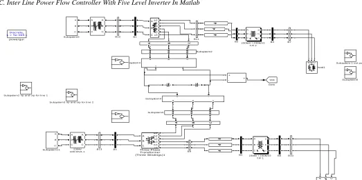
C. Inter Line Power Flow Controller With Five Level Inverter In Matlab
International Journal of Emerging Technology and Advanced Engineering
Website: www.ijetae.com (ISSN 2250-2459,ISO 9001:2008 Certified Journal, Volume 3, Issue 11, November 2013)
179
D. Simulation waveforms in MATLAB/SIMULINK
Fig13.a Injected Voltages for line1 and 2
Fig13.b.Injected currents for line and 2
Fig13.c.Injected active and reactive powers for line1
Fig13.d.Injected active and reactive powers for line 2
International Journal of Emerging Technology and Advanced Engineering
Website: www.ijetae.com (ISSN 2250-2459,ISO 9001:2008 Certified Journal, Volume 3, Issue 11, November 2013)
[image:9.612.50.573.154.508.2]180
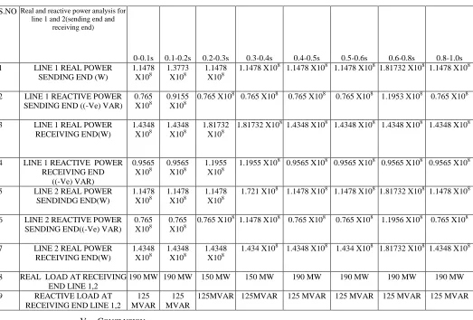
Table 2.
sending and receiving end powers
V. CONCLUSION
The design of an IPFC with five level inverter has presented in this paper. Two different control circuits were designed for generating triggering pulses for five level inverters. The IPFC system with two 5-level in MATLAB/SIMULINK was designed and results validated. The simulation waveforms presented in the paper. The real and reactive powers at sending end and receiving end at different levels are calculated and tabulated
REFERENCES
[1] L.Cera ZanettaJr., R.L.Vasque-Arnez,”Steady- State multi-line
power flow control through the generalized IPFC”, IEEE/PES
[2] M.Venkateswara Reddy,,Dr. Bishnu Prasad Muni,Dr. A.V.R.S.
Sarma “design of controller for an interline power flow controller” PEIE 2011, CCIS 148, pp. 56–61, 2011. © Springer-Verlag Berlin Heidelberg 2011
[3] N. Hingorani and L. Gyugyi, “Understanding FACTS: Concepts
andTechnology of Flexible AC Transmission Systems,” New York, NY: IEEEPress, 2000..Brown, L. D., Hua, H., and Gao, C. 2003. A widget framework for augmented interaction in SCAPE.
[4] S.K. Lim, J. H. Kim, and K. Nam, “A DC-link voltage balancing
algorithm for 3-level converter using the zero sequence current,” IEEE Power Electronics Specialists Conference, Vol. 2, pp. 1083 - 1088, June-July 1999
[5] S. J. Lee, H. Kim, S. Sul, and F. Blaabjerg, “A novel control
algorithm for static series compensators by use of PQR instantaneous power theory,” IEEE Trans. On Power Delivery, Vol. 19, No. 3, pp. 814-827, May 2004. Tavel, P. 2007 Modeling and Simulation Design. AK Peters Ltd.
S.NO Real and reactive power analysis for
line 1 and 2(sending end and receiving end)
0-0.1s 0.1-0.2s 0.2-0.3s 0.3-0.4s 0.4-0.5s 0.5-0.6s 0.6-0.8s 0.8-1.0s
1 LINE 1 REAL POWER
SENDING END (W)
1.1478
X108
1.3773
X108
1.1478
X108
1.1478 X10⁸ 1.1478 X10⁸ 1.1478 X10⁸ 1.81732 X10⁸ 1.1478 X10⁸
2 LINE 1 REACTIVE POWER
SENDING END ((-Ve) VAR) 0.765
X108
0.9155
X108
0.765 X10⁸ 0.765 X10⁸ 0.765 X10⁸ 0.765 X10⁸ 1.1953 X10⁸ 0.765 X10⁸
3 LINE 1 REAL POWER
RECEIVING END(W)
1.4348
X108
1.4348
X108
1.81732
X108
1.81732 X10⁸ 1.4348 X10⁸ 1.4348 X10⁸ 1.4348 X10⁸ 1.4348 X10⁸
4 LINE 1 REACTIVE POWER
RECEIVING END ((-Ve) VAR)
0.9565
X108
0.9565
X108
1.1955
X108
1.1955 X10⁸ 0.9565 X10⁸ 0.9565 X10⁸ 0.9565 X10⁸ 0.9565 X10⁸
5 LINE 2 REAL POWER
SENDINDG END(W)
1.1478
X108
1.1478
X108
1.1478
X108
1.721 X10⁸ 1.1478 X10⁸ 1.1478 X10⁸ 1.81732 X10⁸ 1.1478 X10⁸
6 LINE 2 REACTIVE POWER
SENDING END((-Ve) VAR)
0.765
X108
0.765
X108
0.765 X10⁸ 1.1478 X10⁸ 0.765 X10⁸ 0.765 X10⁸ 1.1956 X10⁸ 0.765 X10⁸
7 LINE 2 REAL POWER
RECEIVING END(W)
1.4348
X108
1.4348
X108
1.4348
X108
1.434 X10⁸ 1.4348 X10⁸ 1.434 X10⁸ 1.81732 X10⁸ 1.4348 X10⁸
8 REAL LOAD AT RECEIVING
END LINE 1,2
190 MW 190 MW 150 MW 150 MW 190 MW 190 MW 190 MW 190 MW
9 REACTIVE LOAD AT
RECEIVING END LINE 1,2 125 MVAR
125 MVAR