Mr.B.Sai Sreenivas1, Dr.Ch.Sai Babu
, Mr.D. Lenine
1
PG-Student, Department of Electrical and Electronics Engg.JNT University, Kakinada, India
2Professor, Department of Electrical & Electronics Engg.& Director (Admissions), JNT University, Kakinada, India
3Assistant Professor, Department of Electrical and Electronics Engg, RGMCET, Nandyal, India-518501.
Abstract - Power factor correction of boost converter is done by using predictive control strategy. In this paper predictive control algorithm is presented based on this algorithm all of the duty cycles required to achieve unity power factor in one half line period are calculated in advance by proportional Integral (PI) controller, the simulation results show that the proposed predictive strategy for PFC achieves near unity power factor. The power factor and input current distortion are analyzed using with control and without control techniques. Simulation results are shows that the power factor is higher than 0.99, and current total harmonics distortion (THD) is smaller than 20% under full load condition.
Index Terms - AC-DC Converter, PI Controller, Predictive control algorithm, flow chart and Simulation Results. .
I. INTRODUCTION
Conventional AC-DC converters are widely used in various applications due to the advantage of high efficiency. These converters draws a non- sinusoidal input ac current which leads to low power factor and injection of harmonics into utility lines. The harmonic currents the converter generates distort the ac line voltage and cause power disturbances. In order to reduce harmonics active and passive filters are being used. The passive filter includes the use of resistors, inductors, and capacitor elements at load side. But these have the disadvantages of low efficiency and high cost. Hence active techniques have gained more importance, which includes use of power electronic switches like IGBT, MOSFET, GTO etc. The high RMS line current also places a high stress on the bridge rectifier and the energy storage capacitor. With increasing demand for more power and better quality, power factor correction becomes an integral part of a switching power supply. Therefore the power factor correction circuits are getting popular and the regulation power range is getting lower.
Power factor correction technique has been widely used in AC to DC switching mode power conversion system. PFC can reduce the harmonics of line current, losses and improve power factor by unity power factor control to meet the requirement of international standards, increase the efficiency and capacity of power systems, and reduce customers‟ utility bills. Numerous methods have been proposed in recent years to achieve unity power factor for the switch-mode power supply. Among them, the boost converter with constant switching frequency is the most popularly used topology. The advantages are:
i) The input current is a smooth waveform, resulting in much less EMI and therefore reduced input filtering requirements;
ii) Current stress in the power switches is lower; iii) The inductor current in the boost converter is the
input current and is therefore easily Programmed; iv) The dc output voltage is higher than the peak of the
input voltage.
In this paper, a new predictive control method of the boost PFC converter which improves the zero-crossing distortion is proposed. The proposed method changes switch on-time according to the magnitude of ac line voltage. The experimental results verify the excellent performance of the proposed method.
II. SYSTEM CONFIGURATION
A. Predictive control based PFC
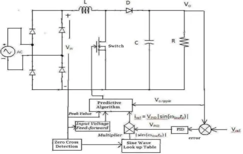
[image:1.595.318.562.481.635.2]In predictive current control technique, all the duty cycles required to achieve near unity power factor are calculated in advance by Proportional Integral Controller (PI). The block diagram of converter circuit with predictive current control is shown in the Figure 1
Fig .1 Diagram of predictive control with boost converter
In this control duty cycle calculation is done using MATLAB programming. Unlike in average current control, predictive control technique consists of only voltage loop and no current loop is present. It has output voltage loop and input feed forward voltage.
B. Circuit Description
International Journal of Emerging Technology and Advanced Engineering
Website: www.ijetae.com (ISSN 2250-2459, Volume 2, Issue 6, June 2012)A boost converter is connected between the rectifier and the load. The boost converter controls the current drawn from the supply voltage with the control action of the switch. The switching action is provided by the predictive control method.
C. Voltage Control Loop
The output voltage (Vout) is sensed and compared with
the reference voltage (Vref) to get error voltage (Verror).
This error voltage is amplified by voltage error amplifier or PID controller to get VPID. The reference current is
generated with the amplitude equal to PID voltage using MATLAB programming. The PI controller in voltage feedback is slow in action because any change in output voltage is sensed and compared with reference voltage.
D. Control Circuit
The control circuit is implemented in MATLAB programming. The output of PID is multiplied with input voltage of the boost converter to get the reference current
iref. The obtained reference current is at the kth switching
[image:2.595.358.504.233.414.2] [image:2.595.51.265.393.547.2]cycle. The reference current at (k+1)th switching cycle can be obtained from the reference current tracking shown in Figure 2 using the following equation.
(1)
Fig.2 Input current waveform and reference current in one Ts.
(Tracking of Reference current)
E. Calculation of Duty Cycle Equations
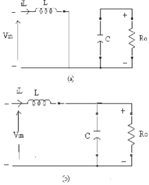
[image:2.595.364.487.447.536.2]The topology of Boost converter is shown in Figure 3 which consists of inductor, diode, capacitor, resistor and power electronic switches like IGBT, MOSFET, GTO control by algorithm for the generation of pulses.
Fig.3 Boost Topology
The proposed predictive PFC algorithm is derived based on the following assumptions
i) Boost converter operates at continuous conduction mode.
ii) The switching frequency is much higher than the line frequency, so the input voltage can be assumed as a constant during one switching cycle.
Based on these assumptions, when the switch S is ON or OFF, the circuit of Figure 4 (a) or (b) are obtained and the inductor current can be described as (1) and (2) respectively,
Fig.4 Boost converter circuit: (a) switch is ON (b) switch is OFF.
Fig.5 Inductor current at ON and OFF period
From figure 4 (a)
(2)
From figure 4 (b)
(3)
The discrete form for the inductor current at the beginning of (k+1)th Switch cycle in term of the inductor current at the beginning of kth switching cycle can be derived from (2) and (3) as
(4)
.
)
sin(
)
1
(
PID
line
k1ref
k
v
t
i
in
L
V
dt
di
L
.
t
k
t
t
k
d
kT
so in L
V
V
dt
di
L
.
t
k
d
kT
s
t
t
k1L
T
k
d
k
V
L
T
k
V
k
i
k
i
L L in s o s}
).
(
1
).{
(
).
(
)
(
)
1
[image:2.595.86.241.654.745.2]achieved, the inductor current should follow the reference current iref(k), which is proportional to the rectified input
voltage. At the same time, the output voltage should follow the reference voltage i.e,
(5) (6) (7)
Substituting (5)–(7) into (4), the duty cycle in kth switching period d (k) can be calculated as
(8)
VPI is the output of the PI regulator. It is determined by
the closed voltage loop.│sin (ωline.tk)│ is the rectified
sinusoidal waveform with the line frequency. It should be noted from (8) that
VPID
has an exact physics meaning that is the peak value of the reference current.Actually, there are two components in (8), expressed as
(9)
The first component d1(k)is
(10)
This component is determined by the input and output voltage equilibrium of Boost topology. Therefore, is defined as voltage equilibrium component (VEC). In the practical PFC system, is not enough due to the following two reasons.First, it can‟t realize the regulation of the output voltage because it is determined by the open loop parameters. Second, it cannot achieve the unity power factor either, because the practical issues, such as the energy stored in or released from the inductor, are not considered.
The second component d2(k) is expressed as
(11)
iL(t)=(1/L) (t).dt, which is in sinusoidal shape. d2(k)
is related to the voltage feedback because the amplitude of the reference current iref is determined by the PI regulator.
After d2(k) is introduced, not only the output voltage can
be regulated to follow the reference, but also the line current can achieve sinusoidalwaveform.
F. Flow Chart for Predictive Control Algorithm
Duty cycle is generated by implementing the duty cycle equation in the MATLAB programing. Step by step programing is given below. Flow chart is given in figure • First the constant parameters like inductance value, switching frequency are initialized.
• The input voltage, output voltage and amplified error voltage are sensed and are embedded into the programing. • The reference current is generated with frequency equal to input line frequency at the present instant. The reference current at next instant is generated at time value one sampling time greater than the present time.
• The duty cycle component is generated based on the derived equations.
Fig.6 Software flowchart for predictive algorithm implementation.
III. SIMULATION RESULTS AND DISCUSSION
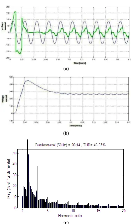
Simulation is performed in MATLAB and results are verified for rectifier without filter and rectifier with filter, Boost converter without any PFC technique.Fig.7. Shows the response of open loop PFC boost converter input voltage with line current, output voltage and line current THD (46.37%) at line voltage is 90V without control technique.
ref
V
k
V
0(
)
)
1
(
)
1
(
k
i
k
i
L ref)
(
)
(
k
i
k
i
L
refTs
L
V
k
i
k
i
V
k
V
V
k
d
ref ref ref ref in ref
(
)
(
1
)
(
)
)
(
.
)
sin(
)
(
PID line kref
k
V
t
i
)
(
)
(
)
(
k
d
1k
d
2k
d
ref in ref
V
k
V
V
k
d
1(
)
(
)
International Journal of Emerging Technology and Advanced Engineering
Website: www.ijetae.com (ISSN 2250-2459, Volume 2, Issue 6, June 2012)(a)
(b)
[image:4.595.328.528.110.250.2](c)
Fig.7. Simulated waveforms (a). Input voltage in phase with line current (b) Output voltage and (c) line current harmonic spectra (%
of fundamental) at line voltage (90V) without control technique.
(a)
(b)
(c)
Fig .8 Simulated waveforms (a). input voltage in phase with line current (b) Output voltage and (c) line current harmonic spectra
(% of fundamental) at line voltage 90V with control technique.
[image:4.595.54.272.115.485.2]Simulation was performed at different values of input voltages and different values of loads for both the converter without control technique and the converter with control technique. The obtained results are compared with each other, which were shown in the table 1.
[image:4.595.319.543.358.477.2]TABLE.1. COMPARISON OF %THDS AND POWER FACTOR WITH DIFFERENT LINE VOLTAGES
TABLE.2. COMPARISON OF %THDS AND POWER FACTOR WITH DIFFERENT LOAD CONDITIONS
IV. CONCLUSION
[image:4.595.60.269.525.732.2]ACKNOWLEDGMENT
I offers my sincere thanks to almighty, my guide ,my parents, EEE department of College of Engineering, JNT University, Kakinada for their immense support and for giving me an opportunity to dedicate my time and energy on this project and gather a lot of knowledge on the subject and present the same as a paper in this journal.
REFERENCES
[1] Wanfeng Zhang, Guang Feng, and Yan-Fei Liu “A Digital Power Factor Correction (PFC) Control Strategy Optimized for DSP” IEEE Transactions on Power Electronics, vol. 19, no. 6, November 2004.
[2] S.Bibian and H.Jin, “Digital control with improved performance for Boost power factor correction circuits,” in Proc. 16th Annu. IEEE Applied Power Electronics Conf. Expo, 2001, pp. 137–143. [3] J.Chen,A.Prodic, R. W. Erickson, and D. Maksimovic, “Predictive
digital current programmed control,” IEEE Trans. Power Electron., vol. 18, pp. 411–419, Jan. 2003.
[4] A.H.Mitwalli, S.B.Leeb, G. C. Verghese, and V.J.Thottuvelil, “An adaptive digital controller for a unity power factor converter,” IEEE Trans. Power Electron., vol. 11, pp. 374–382, Mar. 1996. [5] P.Zumel, A. de Castro, O.Gaecia, T. Riesgo, and J.Uceda,
“Concurrent and simple digital controller of an ac/dc converter with power factor correction,” in Proc. IEEE Applied Power Electronics Conf. Expo, 2002, pp. 469–475.
[6] A. de Castro, P.Zumel, O.Gaecia, T.Riesgo, and J.Uceda, “Concurrent and simple digital controller of an ac/dc converter with power factor correction based on FPGA,” IEEE Trans. Power Electron., vol. 18, pp. 334–343, Jan. 2003.
[7] I.W.Merfert, “Stored-duty-ratio control for power factor correction,” in Proc. IEEE Applied Power Electronics Conf. Expo, vol. 2, 1999, pp. 1123–1129.
[8] “Analysis and application of a new control method for continuous mode Boost converters in power factor correction circuits,” in Proc. IEEE Power Electronics Specialists Conf., vol. 1, 1997, pp. 96–102.
[9] Bhim Singh, Brig N.Singh, Ambrish Chandra, „A Review of Three-Phase Improved Power Quality AC to DC Converters‟. IEEE Transactions on Industrial Electronics, vol. 51, no.3, June 2004 pp,641_659.
[10] A.Pandey, Prof B.Singh, “Comparative Evaluation of Single phase Unity Power Factor ac-dc Boost Converter Topologies.” IEEE proc. November 30, 2004.pp,102_109 [6] B.R Lin and T.Y.Yang “Single-phase half-bridge rectifier with power factor correction ”IEEE Proc_ Electr.Power Appl.Vol.151, No.4.July, 2004.pp,443_450.
[11] Y.Nishida, M.Nakaoka,“Simplified predictive instantaneous current control for single phase and three phase voltage fed PFC converters ”IEEE Proc- Electric .power Appl,vol.144,No 1.July 1996.pp,46_52.
Electronics, Power Systems and Power Factor Correction Techniques.
Dr.Ch. Sai Babu received the B.E from Andhra University (Electrical & Electronics Engineering), M.Tech in Electrical Machines and Industrial Drives from REC, Warangal and Ph.D in Reliability Studies of HVDC Converters from JNTU, Hyderabad. Currently he is working as a Professor in Dept. of EEE, Director (Admission), and ECET Convenor in JNTUK, Kakinada. He has published several National and International Journals and Conferences. His area of interest is Power Electronics and Drives, Power System Reliability, HVDC Converter Reliability, Optimization of Electrical Systems and Real Time Energy Management.
D.Lenine was born in Pondicherry, India in 1978. He received the B.Tech (Electrical& Electronics Engineering) degree from Pondicherry University, India in 2004 and the M.Tech (Electrical Drives and Control) from same University in 2006. In 2006 (October) he joined the Dept. Electrical & Electronics Engineering, R.G.M. College of Engineering and Technology,
Nandyal, as a Assistant Professor. He has