WRL
Research Report 92/5
Piecewise Linear Models
for
Switch-Level Simulation
Russell Kao
We test our ideas by designing, building, and using real systems. The systems we build are research prototypes; they are not intended to become products.
There is a second research laboratory located in Palo Alto, the Systems Research Cen-ter (SRC). Other Digital research groups are located in Paris (PRL) and in Cambridge, Massachusetts (CRL).
Our research is directed towards mainstream high-performance computer systems. Our prototypes are intended to foreshadow the future computing environments used by many Digital customers. The long-term goal of WRL is to aid and accelerate the development of high-performance uni- and multi-processors. The research projects within WRL will address various aspects of high-performance computing.
We believe that significant advances in computer systems do not come from any single technological advance. Technologies, both hardware and software, do not all advance at the same pace. System design is the art of composing systems which use each level of technology in an appropriate balance. A major advance in overall system performance will require reexamination of all aspects of the system.
We do work in the design, fabrication and packaging of hardware; language processing and scaling issues in system software design; and the exploration of new applications areas that are opening up with the advent of higher performance systems. Researchers at WRL cooperate closely and move freely among the various levels of system design. This allows us to explore a wide range of tradeoffs to meet system goals.
We publish the results of our work in a variety of journals, conferences, research reports, and technical notes. This document is a research report. Research reports are normally accounts of completed research and may include material from earlier technical notes. We use technical notes for rapid distribution of technical material; usually this represents research in progress.
Research reports and technical notes may be ordered from us. You may mail your order to:
Technical Report Distribution
DEC Western Research Laboratory, WRL-2 250 University Avenue
Palo Alto, California 94301 USA
Reports and notes may also be ordered by electronic mail. Use one of the following addresses:
Digital E-net: DECWRL::WRL-TECHREPORTS
Internet: [email protected]
UUCP: decwrl!wrl-techreports
Russell Kao
September 1992
Copyright 1992 Russell Kao
Rsim is an efficient logic plus timing simulator that employs the switched resistor transistor model and RC tree analysis to simulate efficiently MOS digital circuits at the transistor level. We investigate the incorporation of piecewise linear transistor models and general-ized moments matching into this simulation framework. General piecewise linear models allow more accurate MOS models to be used to simulate circuits that are hard for Rsim. Additionally they enable the simulator to handle circuits containing bipolar transistors such as ECL and BiCMOS. Nonetheless the switched resistor model has proved to be efficient and accurate for a large class of MOS digital circuits. Therefore it is retained as just one particular model available for use in this framework.
The use of piecewise linear models requires the generalization of RC tree analysis. Un-like switched resistors, more general models may incorporate gain and floating capacitance. Additionally, we extend the analysis to handle non-tree topologies and feedback. Despite the increased generality, for many common MOS and ECL circuits the complexity remains linear. Thus, this timing analysis can be used to simulate, efficiently, those portions of the circuit that are well described by traditional switch level models, while simultaneously simulating, more accurately, those portions that are not.
We present preliminary results from a prototype simulator, Mom. We demonstrate its use on a number of MOS, ECL, and BiCMOS circuits.
Abstract ii
1 Introduction 1
1.1 Verification of Large Digital Designs
: : : : : : : : : : : : : : : : : : :
1 1.2 Organization: : : : : : : : : : : : : : : : : : : : : : : : : : : : : : : :
52 Previous Work in Transient Estimation 7
2.1 Circuit and Timing Simulation
: : : : : : : : : : : : : : : : : : : : : : :
7 2.1.1 Circuit Simulation: : : : : : : : : : : : : : : : : : : : : : : : :
8 2.1.2 Acceleration of Circuit Simulation: : : : : : : : : : : : : : : :
9 2.2 Moment Based Timing Analysis and Simulation: : : : : : : : : : : : : :
13 2.3 Improving Rsim: : : : : : : : : : : : : : : : : : : : : : : : : : : : : :
19 2.4 Comparison and Summary: : : : : : : : : : : : : : : : : : : : : : : : :
203 Piecewise Linear Models 22
3.1 Piecewise Linear Representation
: : : : : : : : : : : : : : : : : : : : : :
22 3.2 Model Restrictions: : : : : : : : : : : : : : : : : : : : : : : : : : : : :
24 3.3 MOS Level-0 Model: : : : : : : : : : : : : : : : : : : : : : : : : : : :
25 3.4 MOS Level-1 Model: : : : : : : : : : : : : : : : : : : : : : : : : : : :
27 3.4.1 Rationale: : : : : : : : : : : : : : : : : : : : : : : : : : : : :
27 3.4.2 Model: : : : : : : : : : : : : : : : : : : : : : : : : : : : : : :
29 3.4.3 Choosing Parameters: : : : : : : : : : : : : : : : : : : : : : :
31 3.5 Bipolar Model: : : : : : : : : : : : : : : : : : : : : : : : : : : : : : :
37 3.6 Second Order Phenomena: : : : : : : : : : : : : : : : : : : : : : : : :
383.7 Summary
: : : : : : : : : : : : : : : : : : : : : : : : : : : : : : : : : :
434 Waveform Approximation 45
4.1 Waveform Approximation
: : : : : : : : : : : : : : : : : : : : : : : : :
46 4.2 Pad´e Approximation: : : : : : : : : : : : : : : : : : : : : : : : : : : :
46 4.3 Practical Considerations: : : : : : : : : : : : : : : : : : : : : : : : : :
49 4.3.1 Order Too Low: : : : : : : : : : : : : : : : : : : : : : : : : :
49 4.3.2 Order Too High: : : : : : : : : : : : : : : : : : : : : : : : : :
50 4.3.3 Unstable Poles: : : : : : : : : : : : : : : : : : : : : : : : : : :
52 4.3.4 Efficiency: : : : : : : : : : : : : : : : : : : : : : : : : : : : :
54 4.3.5 Error Control: : : : : : : : : : : : : : : : : : : : : : : : : : :
54 4.3.6 Frequency Scaling: : : : : : : : : : : : : : : : : : : : : : : : :
56 4.4 Demonstration: : : : : : : : : : : : : : : : : : : : : : : : : : : : : : :
58 4.5 Limitations: : : : : : : : : : : : : : : : : : : : : : : : : : : : : : : : :
62 4.5.1 Unstable Responses: : : : : : : : : : : : : : : : : : : : : : : :
62 4.5.2 Circuits with High Gain: : : : : : : : : : : : : : : : : : : : : :
63 4.6 Summary: : : : : : : : : : : : : : : : : : : : : : : : : : : : : : : : : :
665 Moment Computation 68
5.1 Background
: : : : : : : : : : : : : : : : : : : : : : : : : : : : : : : :
69 5.2 Moment Computation for Leaky Resistor Trees: : : : : : : : : : : : : :
70 5.3 Leaky Trees of Three Terminal Networks: : : : : : : : : : : : : : : : :
73 5.4 Series-Parallel Combination: : : : : : : : : : : : : : : : : : : : : : : :
75 5.5 Coupled Clusters: : : : : : : : : : : : : : : : : : : : : : : : : : : : : :
76 5.6 Relaxing Network Restrictions: : : : : : : : : : : : : : : : : : : : : : :
80 5.6.1 Node and Branch Tearing: : : : : : : : : : : : : : : : : : : : :
82 5.6.2 Non-Leaky Tree Topologies: : : : : : : : : : : : : : : : : : : :
84 5.7 Partial Evaluation of Floating Capacitive Coupling: : : : : : : : : : : :
86 5.8 Summary: : : : : : : : : : : : : : : : : : : : : : : : : : : : : : : : : :
906 Detecting Region Changes 91
6.2 Overview of Root Finding
: : : : : : : : : : : : : : : : : : : : : : : : :
93 6.3 Order Reduction: : : : : : : : : : : : : : : : : : : : : : : : : : : : : :
94 6.4 Finding Roots: : : : : : : : : : : : : : : : : : : : : : : : : : : : : : :
94 6.4.1 One Pole: : : : : : : : : : : : : : : : : : : : : : : : : : : : : :
95 6.4.2 Two Poles: : : : : : : : : : : : : : : : : : : : : : : : : : : : :
95 6.4.3 Three Poles: : : : : : : : : : : : : : : : : : : : : : : : : : : :
96 6.5 Root Polishing: : : : : : : : : : : : : : : : : : : : : : : : : : : : : : :
100 6.6 Measurements: : : : : : : : : : : : : : : : : : : : : : : : : : : : : : :
102 6.7 Summary: : : : : : : : : : : : : : : : : : : : : : : : : : : : : : : : : :
1037 Evaluation 105
7.1 Extending Switch-Level Simulation
: : : : : : : : : : : : : : : : : : : :
106 7.1.1 CMOS: : : : : : : : : : : : : : : : : : : : : : : : : : : : : : :
106 7.1.2 ECL: : : : : : : : : : : : : : : : : : : : : : : : : : : : : : : :
110 7.1.3 BiCMOS: : : : : : : : : : : : : : : : : : : : : : : : : : : : : :
115 7.2 Performance Compared to Switch-Level Simulation.: : : : : : : : : : :
120 7.3 Summary: : : : : : : : : : : : : : : : : : : : : : : : : : : : : : : : : :
1268 Conclusion 127
A MOS Level-1 Threshold 132
B MOS Level-1 Polytopes 134
C Linearization of Bipolar Transistor Capacitances 136
D Optimal Frequency Scaling 139
D.1 Algorithm
: : : : : : : : : : : : : : : : : : : : : : : : : : : : : : : : :
139 D.1.1 Implementation: : : : : : : : : : : : : : : : : : : : : : : : : :
140 D.2 Efficiency: : : : : : : : : : : : : : : : : : : : : : : : : : : : : : : : :
1421 Execution Time Required to Generate Waveform Approximations.
: : : :
54 2 Benchmark Statistics.: : : : : : : : : : : : : : : : : : : : : : : : : : :
58 3 Decrease in Efficiency with Increasing Capacitor Levels.: : : : : : : : :
88 4 Voltage Error at Estimated Root of Boundary Waveform.: : : : : : : : :
101 5 Time Error of Boundary Waveform Root Estimate.: : : : : : : : : : : :
101 6 Number of Iterations for Root Polishing.: : : : : : : : : : : : : : : : :
102 7 Average Number of Cycles for Root Finding.: : : : : : : : : : : : : : :
102 8 Pole Configurations for Root Finding.: : : : : : : : : : : : : : : : : : :
103 9 Execution Time of Example Circuits (seconds).: : : : : : : : : : : : : :
108 10 Simulator Performance on Ring Oscillators.: : : : : : : : : : : : : : : :
121 11 Mom Execution Profiles for Various Benchmark Circuits.: : : : : : : : :
123 12 Mom’s Simulation Statistics for Ring Oscillators.: : : : : : : : : : : : :
1241 Simulation Hierarchy
: : : : : : : : : : : : : : : : : : : : : : : : : : :
1 2 Circuit Level Representation: : : : : : : : : : : : : : : : : : : : : : : :
2 3 Gate Level Representation: : : : : : : : : : : : : : : : : : : : : : : : :
3 4 Resistive Switch Representation: : : : : : : : : : : : : : : : : : : : : :
4 5 Node Decoupling: : : : : : : : : : : : : : : : : : : : : : : : : : : : :
12 6 Voltage Ranges: : : : : : : : : : : : : : : : : : : : : : : : : : : : : : :
12 7 RC Tree: : : : : : : : : : : : : : : : : : : : : : : : : : : : : : : : : :
14 8 Switched Resistor Model: : : : : : : : : : : : : : : : : : : : : : : : :
15 9 Decomposition of Circuit into Clusters.: : : : : : : : : : : : : : : : : :
16 10 Rsim’s Event Driven Simulation Algorithm.: : : : : : : : : : : : : : : :
16 11 Multiple Segments per Logical Transition.: : : : : : : : : : : : : : : : :
20 12 Switched Resistor Model.: : : : : : : : : : : : : : : : : : : : : : : : :
23 13 Hyperplane Subdivides Space into Regions of Operation.: : : : : : : : :
23 14 Response of Level-0 Inverter Compared to SPICE.: : : : : : : : : : : :
26 15 MOS I-V Characteristics With and Without Velocity Saturation: : : : : :
28 16 Linearization of Transconductance for LargeV
gs: : : : : : : : : : : : :
29 17 Piecewise Linear MOS Model: Saturated Region: : : : : : : : : : : : :
29 18 Piecewise Linear MOS Model: Linear Region.: : : : : : : : : : : : : :
30 19 Piecewise Linear MOS Model: Off Region.: : : : : : : : : : : : : : : :
30 20 Piecewise Linear vs SPICE I-V Characteristics:V
gs = 3,4, and 5 volts,SPICE Level-2 models for MOSIS 2
Process.: : : : : : : : : : : : : :
31 21 Piecewise Linear vs SPICE I-V Characteristics: SPICE Level-3 models forIntroduction
1.1
Verification of Large Digital Designs
Over the past few decades the number of transistors it is possible to incorporate into a single digital integrated circuit (IC) has risen at a breathtaking pace. Unfortunately, as the complexity of integrated circuits increases, so does the likelihood of design errors and the difficulty of detecting and identifying those errors. Consequently, designers have become dependent upon simulation programs to predict the behavior of ICs before they are actually fabricated. These programs make it possible to verify that an IC conforms to logical and timing specifications before committing the vast resources necessary to build it.
In order to deal with the staggering complexity of designs consisting of hundreds of thousands of transistors, a hierarchy of simulation tools and techniques has evolved (Figure 1). In general, lower levels of simulation utilize more detailed descriptions of
increasing speed
Circuit level
increasing accuracy
Device level
Switch level
Gate level
Functional level
the design and provide greater accuracy and flexibility. However, this increased accuracy is usually achieved at the expense of decreased efficiency, limiting the size of designs it is possible to simulate. In contrast, higher level simulators utilize simplified higher level models to represent the behavior of collections of lower level objects. Because higher level models abstract away many lower level details, higher level simulators can simulate larger designs more efficiently. However, the assumptions made in formulating the higher level models often compromise their accuracy and flexibility. Thus, tradeoffs exist for every level of simulation. The result is that the design process usually includes simulation at multiple different levels.
Because the focus of this thesis is switch-level simulation we will narrow our discussion to just the three middle levels of Figure 1 . Immediately below the switch-level is circuit
level simulation. Circuit simulators[Nag75, WJM+
73] represent the IC as a network of lumped, possibly nonlinear, transistors, resistors, inductors, capacitors, and current and voltage sources (Figure 2). Kirchoff’s voltage and current laws are used to formulate a
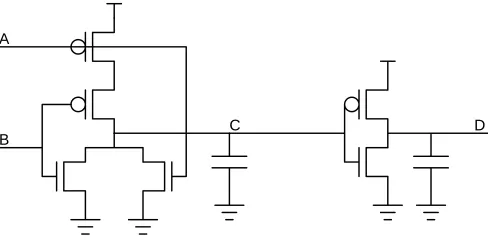
D C
[image:15.612.210.454.390.513.2]B A
Figure 2: Circuit Level Representation
logic gates.
In contrast, gate level simulators represent the IC as a network of gates (Figure 3). A
D = C C = (A + B)
D C
B A
Figure 3: Gate Level Representation
gate is a higher level object that represents a collection of transistors. Each gate interacts with the rest of the circuit via a set of unidirectional input and output terminals. A gate observes the state of wires attached to its inputs, and sets the state of wires attached to its output. Wire states are represented by Boolean values, and a gate’s behavior is modeled by a Boolean function that determines the output value as a function of the input values. The primary advantage of gate level simulation is efficiency. Logic simulation programs running on contemporary workstations can simulate up to a million logic transitions of a logic gate in a second. However, there are disadvantages. First of all, the circuit must be partitioned into a number of pre-characterized gates that exhibit unidirectional behavior. While this is readily done for gate arrays and standard cell designs (after all, these designs are composed from gates selected from libraries) custom designs often contain structures (for example, the MOS pass transistor structure) whose behavior is bidirectional and consequently is not readily modeled by the gate abstraction. Secondly, the characterization of the logical and timing behavior of gates is usually performed manually and can be time consuming and error prone.
Switch-level simulation[Bry80, Ter83, RT85b, DvGdG85, Sch85] is a relatively recent innovation which attempts to strike a balance between gate and circuit level simulation. The circuit is described as a network of transistors that are simply modeled by voltage controlled switches. Depending upon the particular approach, each switch has associated with it either a strength[Bry80] or a resistance[Ter83, RT85b] representing the current driving capabilities of the transistor (Figure 4). Because the circuit isn’t partitioned into unidirectional gates, switch level simulators eliminate the pre-characterization step1and can simulate a wider variety of circuits than gate level simulators (including those exhibiting
1Instead of pre-characterizing every different logic gate the user only needs to pre-characterize the two
B A
D C
Figure 4: Resistive Switch Representation
bidirectional behavior). Simultaneously, the simplified circuit models allow switch-level simulators to be more than three orders of magnitude faster than circuit simulators.
Of course, limitations can arise from the use of overly simplistic transistor models. The switch model was initially developed for the simulation of MOS digital circuits, and works well for the static MOS logic which makes up most of a typical digital MOS IC. Occasionally, however, there are small portions of an IC whose behavior is not well modeled by a network of switches. Typically, these portions must be simulated at the circuit level, thus complicating the verification of the design. Furthermore, resistive or multi-strength switches are poor models for the behavior of bipolar transistors in ECL circuits. Although switch-level models have been extended to allow the simulation of bipolar transistors[HS87, SYH88, KAHS88], real ECL and BiCMOS designs occasionally include circuit techniques (for example, diode decoders, leaker resistors, current source sharing) that foil approaches based upon classical ECL current steering trees.
To address these shortcomings, this thesis attempts to extend the capabilities of switch-level simulation. Noting that the switched resistor model is just a particular piecewise linear model, we investigate the incorporation of more general piecewise linear transistor models into the switch-level framework.2 Several considerations motivate the use of piecewise
2Pillage[Pil89] suggested the incorporation of piecewise linear models and moment analysis into a circuit
linear models. First, we would like to incorporate more sophisticated MOS models in order to simulate the behavior of MOS circuits that cannot be simulated by the use of switched resistors (for example RAM sense amplifiers). Second, we would like to be able to simulate bipolar transistors which are strongly nonlinear but which seem to be adequately described by fairly simple piecewise linear models[KAHS88]. Meanwhile, we would like to give up as little efficiency as possible. Switch-level simulation has proven itself useful for simulating the large majority of MOS digital circuits and it would be best if we could pay for additional generality for only those portions of the circuit where it was needed. To this end the simulator provides the user with a selection of transistor models of which the switched resistor model is one choice. It turns out that the RC tree analysis techniques can be generalized to efficiently handle trees of our more general piecewise linear devices with only a modest degradation of efficiency. The resulting simulator, Mom, is a mixed mode simulator that extends the capabilities of switch-level simulation in the direction of circuit simulation.
1.2
Organization
The next chapter describes previous work in estimating the transient response of digital circuits. In particular the approach taken by circuit simulators (e.g. SPICE) is compared with that taken by switch-level simulators (e.g. Rsim). Although much work has gone into trying to speed up circuit simulation, we approach the problem from a different perspective. That is, rather than starting with a simulator that is accurate and trying to improve its efficiency, we start with a simulator that is efficient and try to improve its accuracy.
The efficiency and flexibility of Mom are strongly dependent upon the choice of piece-wise linear models. Chapter 3 discusses restrictions that are placed upon the models to preserve efficiency. It also explores the utility of simple piecewise linear models and demonstrates that even simple models can greatly extend the capabilities of switch-level simulation.
experience with moments matching waveform approximation. Although the procedure has been extensively explored by others, there are a number of practical considerations unique to our application.
Chapter 5 describes extensions to RC tree analysis that allow it to handle piecewise linear models. It is demonstrated that as long as the topology of the transistors is a tree, and as long as there is no feedback, the complexity of the analysis remains
O
(n
). It turns outthat most MOS and ECL circuits meet these restrictions. However, the analysis can also be extended to handle non-tree topologies and feedback. Although the extensions are not as efficient they only need to be used for those portions of the circuit that don’t meet the restrictions.
The introduction of piecewise linear models greatly complicates the task of detecting when devices switch. Ultimately, the problem boils down to finding the smallest, positive root of a multiple-pole exponential waveform. Chapter 6 discusses the techniques used to solve this problem efficiently.
Previous Work in Transient Estimation
Many different approaches have been proposed for estimating the transient response (and hence delay) of digital circuits. Here, we will review and contrast two prevalent approaches. One approach is exemplified by circuit and timing simulators. This approach is character-ized by the use of nonlinear device models and incremental time numerical integration. A second approach has been taken by some MOS timing analyzers and switch-level simula-tors. This approach employs linear device models and moment analysis.
2.1
Circuit and Timing Simulation
Circuit and timing simulation have evolved continuously over the past few decades. The “second generation1” simulators[WJM+
73, Nag75] reached maturity during the mid 1970’s. These simulators have since achieved widespread acceptance and are now regarded as the classic “circuit simulators”. However, as ICs increased in size, the circuit simulators were found to require excessive amounts of computer memory and time. Consequently, a “third generation” of simulators emerged which attempted to accelerate the transient simulation of large digital ICs.
1Hachtel and Sangiovanni-Vincentelli[HSV81] have found it to be convenient to distinguish between three
generations of simulators.
2.1.1
Circuit Simulation
Circuit simulators represent the IC as a network of lumped, possibly nonlinear transistors, resistors, inductors, capacitors, and current and voltage sources. The equations relating the terminal voltages and currents of the network elements are combined with Kirchoff’s voltage and current laws to produce a set of coupled nonlinear differential equations describing the electrical behavior of the network. These equations can be written:
f
(x
(t
)x
0(
t
)t
)=0 (1)x
<n;f
():<n<n<!<nwhere
x
(t
)is a (time varying) vector of network variables (voltages and currents),x
0(
t
)is its time derivative, and
t
is time. The transient response of the network is simply the solution of these equations fort >
0 subject to the initial conditions:x
(t
=0)=x
0.Incremental time numerical integration is used to solve the equations. The procedure involves advancing time in steps:
t
k+1=
t
k +h
kt
0 =0 (2)(
h
k is the size of thek
th step) and computing the response at each step. That is at each time step a linear multistep integration formula of the general form2x
(t
k +1)=
p
X
i=0
a
ix
(t
k ;i)+
h
kp
X
j=;1
b
jx
0 (t
k;j
) (3)
is used to eliminate
x
0(
t
) from Equation (1). This yields a system of coupled nonlinearalgebraic equations,
g
(x
(t
k +1))=0 (4)
which is solved using Newton-Raphson iteration. That is, starting from an initial guess:
x
0(
t
k +1)=
x
(t
k), successively improved estimates are computed:for
i
=0123:::
beginx
i+1 (t
k+1 )=
x
i
(
t
k +1);
g
(x
i(t
k +1))
g
0 (x
i(t
k+1 ))
(5)
end (6)
2The coefficients,
a
iand
b
i, are chosen to ensure that the formula is satisfied exactly ifx
(
t
)is a low order(
g
0()is the Jacobian of
g
()) until some convergence criterion is met:x
i+1 (t
k+1 );
x
i
(
t
k +1)
<
(7)(
is some error tolerance). The time step,h
k is carefully chosen to control the local truncation error of the integration formula (3). Time step selection involves a compromise because smaller step sizes decrease both the error and simulation efficiency.Flexibility and accuracy are the primary advantages of circuit simulation. The equation formulation places few restrictions on the network’s topology, and the ability to handle nonlinear network elements allows accurate transistor models. Furthermore, the numerical integration procedure allows the computation of the detailed time step by time step behavior of any electrical variable in the circuit. The accuracy of the integration algorithms is limited only by numerical considerations which are almost always insignificant compared to the precision with which components can be fabricated on an IC.
The disadvantage of circuit simulation is the inefficiency that results from processing the entire circuit simultaneously. At each time step circuit simulators compute multiple Newton-Raphson iterations, each of which requires the formulation and inversion of the Jacobian. However, the inversion of the Jacobian of an entire IC can be prohibitively expensive. Even using sparse techniques, the inversion of circuit matrices has been empirically observed to grow superlinearly (for example,
O
(n
1:5
)[Kun86]) with the circuit size. Furthermore,
because a single time step is chosen for the entire circuit, the step size is necessarily limited by the accuracy requirements of the fastest moving subcircuit. Thus tiny time steps must be taken for the entire IC if a single gate is switching rapidly, even if nothing else in the rest of the IC is switching at all!
2.1.2
Acceleration of Circuit Simulation
selection of different time steps for different portions of the IC. Third, it became possible to bypass completely the analysis of latent subcircuits, that is subcircuits that weren’t actively switching. We will describe three common techniques that were used to decompose the circuit equations (4): circuit tearing, relaxation, and forward Euler integration.
Circuit Tearing
Macro[RSVH79] and Slate[YHT80] employed circuit tearing techniques to reduce the Jacobian to bordered block diagonal form. Once in this form the system of equations could be solved in two steps. First, each of the blocks was solved independently. Second, the overall solution was assembled from the individual solutions. However, only the non-latent blocks needed to be processed at any particular step. If the state of a block changed little between the last two time steps or Newton Raphson iterations the block was declared latent and the solution from the previous time step or Newton Raphson iteration was simply reused. Thus, the needless reevaluation of subcircuits that were not changing was bypassed much in the same way that SPICE bypassed devices[Nag75].
Relaxation
MOTIS[CGK75] was the first of the so called “timing simulators” that utilized restricted cir-cuit models, nonlinear relaxation, and time advancement integration. When certain restric-tions were placed on the circuit (including no inductors, no floating capacitors, a grounded capacitor at each node3, unidirectional coupling from an MOS transistor’s gate to its source
and drain, and appropriate ordering of the nodes) the Jacobian became nearly lower block
triangular and, for sufficiently small step sizes, diagonally dominant. These characteristics
make it efficient to invert the Jacobian using a form of Gauss-Jacobi relaxation. Nonlinear Gauss-Jacobi relaxation essentially decomposes the system of equations (4) into a set of scalar equations by treating all non-diagonal entries of the Jacobian as if they were zero. That is, starting with an initial guess,
x
0(
t
k +1)=
x
(t
k), each succeeding relaxation iterate,x
i+1 (t
k+1
), is assembled by solving the
j
th equation,g
j, for thej
th component ofx
,x
j,3A “floating” capacitor is a capacitor with neither terminal connected to ground or a power supply. A
assuming that all other components,f
x
l :l
6=j
gare fixed at their values from the previousiteration.
for
i
=0123:::
beginfor
j
=123:::n
beginsolve for
x
i+1j (
t
k +1):
g
j(x
i1(
t
k +1)
x
i2(
t
k +1)
:::x
ij ;1(
t
k +1)
x
i+1
j (
t
k +1)
x
ij +1(
t
k +1)
:::x
in(t
k +1))=0
end end
In principle, the innermost loop uses Newton-Raphson iteration to solve each of the scalar nonlinear equations, and the outermost loop computes successive relaxation iterations until the
x
i converge (Equation (7)). However, the time advancement algorithms utilized only one relaxation step per time step and only one Newton-Raphson step per relaxation step because that was shown to be sufficient to guarantee convergence. MOTIS pioneered the use of time advancement integration algorithms and, in doing so, avoided both sparse Gaussian elimination and Newton-Raphson iteration.MOTIS was followed by a number of simulators that explored variations of the relax-ation procedure. Event-driven techniques from logic simulrelax-ation were used by SPLICE1 [New79] to 1) dynamically order the equations thereby achieving faster convergence and 2) bypass the evaluation of latent nodes. Problems with reliability motivated the investigation of alternatives to Gauss-Jacobi time advancement, including Gauss-Seidel[New79], and
Modified Symmetric Gauss-Seidel[DMNSV83] algorithms. Additionally, it was realized
that relaxation could be applied at different levels, including at the linear equation level (MOTIS2[CS84]), the nonlinear equation level (SPLICE 1.6[Sal83]) and the waveform level (Relax[LSV82]).
Forward Euler Integration
the formulation:
Cv
0(
t
)=i
(v
(t
)) (8)v
<n;C
<n<n;i
():<n !<nwhere
v
(t
)is a (time varying) vector of node voltages (measured with respect to ground),v
0(
t
) is its time derivative,C
is a diagonal matrix of node to ground capacitances, andi
()gives the currents injected into each node by the non-capacitive elements. SinceC
isdiagonal, it is trivially inverted, and Forward Euler integration is used to predict the value of
v
at some time step,h
n, in the future:v
(t
n +1)=
1
h
nC
;1
i
(v
(t
n)) (9)Note that this formulation decouples the nodes. To predict the future voltage of a node,
N
, (see Figure 5) it is necessary to compute the currents through only those devices directly attached toN
(r
2 andr
3) No matrix formulation or inversion is required. Furthermore,r1 r2 r3 r4
N
Figure 5: Node Decoupling time steps can be selected independently.
The approach taken by Elogic, SPECS, and WATSWITCH[RVB88] was to partition voltage into a small number of disjoint ranges (Figure 6). Then the time step for a node
range 1 range 2 range 3 range 4
0 v range 0 1 v 5 v 4 v 3 v 2 v
Figure 6: Voltage Ranges
value to just outside its present range. An event was scheduled for a node for the time when its voltage crossed into an adjacent range. When this event fired, the current through all devices attached to the node were updated and new waveforms were computed for all nodes connected to those devices. Thus, simulation proceeded on an event–driven basis and the evaluation of latent nodes was bypassed.
Later versions of SPECS associated the voltage ranges with the devices rather than the nodes and formalized the simulation in terms of piecewise linear voltages and piecewise constant current device models[RV87]. Furthermore, extensions were made to include floating capacitors and inductors[VFR90]. ADAPTS[SNGR91] further generalized the approach by dynamically selecting each device’s voltage ranges (and, hence, the step size) based upon an analytical model for the device and the accuracy requirements of the overall simulation.
In general the third generation simulators achieved speed-ups of up to two orders of magnitude over the classic circuit simulators. However, their restricted circuit models and problems with reliability have impeded their widespread acceptance. Furthermore their speedups, although impressive, are fundamentally limited by the use of numerical integration. Time advancement numerical integration requires that time be advanced in steps whose size is limited by the need to maintain accuracy and, in some cases, stability.
2.2
Moment Based Timing Analysis and Simulation
In spite of the large amount of work invested in trying to speed up circuit simulation a large gap remained between the timing simulators and the gate level simulators. Consequently in the early 1980’s a new form of simulator was devised to fill this gap, the switch-level simulators. One of these, Rsim[Ter83, Hor83], took a fundamentally different approach to transient estimation from the circuit and timing simulators. Instead of modeling the behavior of devices using nonlinear models and computing the response of the networks using
numerical integration, Rsim modeled the behavior of devices using simple linear models
Moment analysis originated in the late 1940’s when Elmore[Elm48] utilized the first and second moments of the impulse response of a linear amplifier to estimate its step response. In general, the
k
th moment of the (presumed causal) impulse response,h
(t
), is defined:c
m
k = Z1
0
t
k
h
(
t
)dt
(10)Elmore found that the quantities( p
2
m
c2; c
m
2 1)andc
m
1were good estimates of the stepresponse’s rise time and the delay to its 50% point, respectively. The delay estimate became known as the Elmore delay.
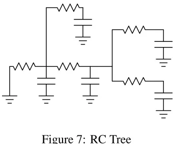
[image:27.612.246.417.376.517.2]Interest in the application of moment analysis to the modeling of delays in MOS digital integrated circuits was sparked by Penfield and Rubinstein[PR81] who modeled the delay of polysilicon interconnect by the step response of RC trees. An RC tree was defined to be a tree of resistors with one grounded node and grounded capacitors at the other nodes (Figure 7). RC trees were particularly interesting because interconnect usually took the
Figure 7: RC Tree
form of trees and because trees were easy to analyze. Penfield and Rubinstein described a computationally efficient algorithm for computing the first moment of RC trees and derived waveform bounds for the step response based upon the single time constant approximation. Although this work was initially intended to model the delays of linear interconnect, it was soon used by a number of MOS timing analyzers[Put82, Jou83] to model the delays of networks of nonlinear MOS transistors. Horowitz[Hor83] more carefully justified this approach by deriving nonlinear one and two time constant waveform estimates and bounds. He then retrofitted his nonlinear timing models into an existing switch-level simulator4,
Rsim[Ter83]. Because this thesis is essentially an extension of Rsim we next describe in greater detail the algorithms used by Rsim.
As mentioned in the introduction, Rsim models transistors with the simple resistive
switch consisting of the series combination of a resistor and a voltage controlled switch
(Figure 8). The resistor models the current driving capabilities of the MOS transistor and
Vd
Vs Vg
V
d V
s V g
Figure 8: Switched Resistor Model
is sized according to the width and length of the transistor. The switch is either on or off and is controlled by the gate voltage measured with respect to ground. If (for an NMOS transistor) the gate voltage is greater than half the power supply voltage then the switch is closed (current flows). Otherwise the transistor is an open circuit. It is assumed that no DC current flows into the gate and, aside from the gate’s control of the switch, there is no coupling between the gate and the channel. As with the early third generation simulators, floating capacitors are disallowed and modeled by “equivalent” capacitances to ground.
Replacing on transistors by resistors and off transistors by open circuits usually results in a partition of the original circuit into a large number of small, mutually independent subcircuits known as stages or clusters (Figure 9). Because clusters are decoupled, their responses can be computed independently. Thus in order to compute the transient response of the overall circuit it is only necessary to analyze those clusters that are actively switching at each point in time. Rsim uses an event-driven simulation algorithm to schedule the evaluation of active clusters thereby avoiding the analysis of latent clusters (Figure 10).
D cluster 2 C
cluster 1 A (0)
B (0) C (1) D (0)
Figure 9: Decomposition of Circuit into Clusters.
To compute the response of a cluster Rsim uses moment analysis instead of numerical integration. Moment analysis is a two step process that involves, first, the computation of moments from the network followed by the generation of waveform estimates from those moments. Moments were computed using a procedure equivalent to finding successive DC solutions for the network. Particular advantage was taken of the tree structure possessed by most circuits. Sparse matrix formulation and sparse Gaussian elimination were bypassed in 1. Through the use of an event queue, select the next device to switch. Advance the
simulation time to the time of this event.
2. Construct the cluster. That is, collect all nodes affected by this switching event. 3. Compute the response of the cluster resulting from the switching event.
4. Reschedule all MOS transistors affected by this cluster. That is, examine every transistor with a gate terminal attached to the cluster and schedule an event for it if the new response causes it to switch some time in the future.
Figure 10: Rsim’s Event Driven Simulation Algorithm.
favor of simpler tree analysis techniques whose complexity was guaranteed to be
O
(n
)inthe size of the cluster. In the rare case that non-tree topologies were encountered, heuristics5
were used to simply delete resistors closing loops in order obtain an approximate solution.
5It was noted that the most commonly occurring case of loops was created by CMOS transmission gates.
In his thesis Horowitz showed that waveform estimates for linear RC networks, could be obtained from the moments by assuming that the system function was of the general form6
V(
s
)=1
(1+
1s
)(11) for single time constant estimates, or:
V(
s
)=(1+
s
z) (1+s
1)(1+s
2)(12) for two time constant estimates. Then, the parameters,
1, 2, and z, were obtained bymatching (among other things) the low order moments of the system function with those computed from the circuit. In the time domain, these one and two time constant estimates took the forms:
v
(t
)=e
;t=1and (13)
v
(t
)= (z;1)e ;t=1
+(
2;z)e ;t=2
)
2;
1 (14)
respectively.
However, MOS transistors are nonlinear. Horowitz showed that the single time constant estimate of the response of a nonlinear NMOS network was:
v
(t
)= 8 < :1;tanh(
t=
1)v
(t
)fallingt
t+1
v
(
t
)rising(15) where
1 was the first moment of the network obtained by replacing each transistor by aresistor of resistance:
R
eff=2
k
(V
dd;V
t)(16) (where
k
=C
oxW=L
is the device transconductance parameter andLWC
oxandV
tare parameters of the quadratic MOS model[MK77, HJ83]).
However, switch-level simulators do not require the computation of the waveform but rather only the delay to the 50% point. For linear networks, the delay can be computed
by multiplying the first moment7 by ;ln(1
=
2). For NMOS networks the delay can becomputed by multiplying the first moment by tanh;1
(1
=
2)for falling transitions and 1 forrising transitions. Thus although the step response of MOS-capacitor trees is not identical to the step response of resistor-capacitor trees, the computation of single time constant delay estimates of MOS trees could be made identical in form to that of resistor trees by choosing the resistor values appropriately. It was precisely this observation that justified the use of the switched resistor model. Unfortunately, Horowitz found no corresponding relationship between linear and nonlinear two time constant delay estimates.
Numerous extensions to the approach of Penfield, Rubinstein, and Horowitz have been suggested. A number of researchers have investigated the extension of linear mo-ment analysis to circuits more general than RC trees, including RC trees with multiple sources[Chu88, RT85a], RC meshes[Wya85, LM84], and floating capacitors and con-trolled sources[SZ87]. Also explored was the use of higher order estimates to model the non-monotonic waveforms arising from linear[RT85a] and nonlinear[Chu88] charge sharing.
However, many of the extensions to linear moment analysis were superceded by the recent discovery[Hua90, Cha91] that single time constant delay estimation was just a special case of the more general moments matching procedure developed to solve the model order reduction problem of linear control theory. In 1956 Paynter[Pay56] applied the Pad´e approximation to the approximation of system functions. That approach constructs approximations of arbitrary order by matching low order moments. Pillage, Rohrer, and Huang[PR90, Hua90] combined general Pad´e approximation with standard circuit equation formulation and analysis techniques from circuit simulation to generate arbitrarily high order estimates of the responses of general lumped linear networks. They demonstrated the application of those techniques to the estimation of the responses of linear interconnect and the estimation of the poles and zeros of linearized models of operational amplifiers.
7For the linear single time constant approximation the result of matching the first moment of Equation (11)
2.3
Improving Rsim
Switch-level simulation has its limitations. A common scenario is that the simulator can simulate 99.9% of a large circuit, although for small portions the simulator fails to produce even a correct logical result. Sometimes those failures don’t interfere with the verification of the circuit. For example, the output of a voltage reference generator can be manually fixed in a switch-level simulation after being verified using SPICE. Unfortunately the simulator’s failure sometimes hinders the verification of the design. For example, Rsim’s inability to deal with sense amplifiers makes it difficult to check the logical correctness of RAMs.8
However, most of such a circuit can be simulated at the switch-level. If it were possible to increase the generality of the simulator just for certain small portions of the circuit it would be possible to validate the entire design.
Piecewise linear models promise to give the user the ability to select different accuracies for different parts of the circuit.9 For the RAM described above only small portions need to
be simulated with more accurate models while the majority of the circuit can be simulated using switch-level models. In principle, if a simulator were designed such that the additional complexity was paid for only when it was used, it would be possible to simulate those circuits with only a moderate impact on the overall efficiency. Since the switched resistor model is a piecewise linear model, it appears promising to simply extend Rsim’s simulation framework to allow more general piecewise linear models.
Although Rsim’s basic simulation framework can be retained, extensive changes are required. One change involves the representation of node state. Rsim takes advantage of the fact that most digital MOS gates have logic swings from one power supply rail to the other and switching thresholds at the midpoint. Therefore Rsim represents the state of nodes using the Boolean values 0 and 1 and describes state transitions using just the delay and slope at the 50% point. However, because Mom must simulate a wider variety of circuits, it can make fewer assumptions about their properties. For example, ECL circuits have multiple nonoverlapping voltage swings which make it impossible to establish a one to one
8Although each of the individual pieces of a RAM is usually verified using a circuit simulator, it is still
useful to verify the logical functionality of the entire RAM using a switch-level simulator in order to confirm that the decoders have been hooked up properly, that the data hasn’t been inadvertently inverted, etc.
9The present version of the simulator depends upon the user to manually choose transistor models.
correspondence between a logical value and a voltage. To avoid building in assumptions about particular logic families, Mom utilizes real voltages to represent the state of nodes and waveforms to describe the shape of transitions.
Although the switched-resistor model is a piecewise linear model, more general piece-wise linear models have attributes which necessitate extending the switch-level framework. First, while the switched-resistor model only has two regions of linearity, a more general piecewise linear model can have any number of regions. Devices with more regions are more difficult to schedule. They also generate additional events which cause logic tran-sitions to be made up of multiple segments instead of just a single segment (Figure 11). Second, while the linear circuit describing the behavior of the switched-resistor model
Rsim: Mom:
Figure 11: Multiple Segments per Logical Transition.
(when it is on) is just a resistor, more general piecewise linear models can have more com-plex circuit models which include voltage, current, and dependent sources. More comcom-plex circuit models complicate the estimation of a circuit’s response. Not only are the wave-form estimates more complex, but the procedures for computing moments require more sophistication.
Unfortunately these changes degrade the efficiency of the simulator. Simpler models yield more efficient simulations, and there are strong incentives to use models that are as simple as possible. The next chapter considers the constraints that must be placed upon piecewise linear models in order to preserve efficiency. Additionally it explores the capabilities of simple piecewise linear models.
2.4
Comparison and Summary
topology, utilizes general nonlinear transistor models, and employs time advancement numerical integration to solve the circuit equations. The advantages of circuit simulation are its accuracy and generality. The disadvantage of circuit simulation is its inefficiency. The general models and topologies require algorithms whose execution time grows superlinearly with the circuit size, making their use impractical for large ICs.
The classic circuit simulators were followed by a third generation of simulators which focused on the acceleration of the transient simulation of large ICs. These approaches were based upon the use of simplified circuit models and the decomposition of the circuit into pieces that could be analyzed independently. Decomposition accelerates simulation by reducing the size of the systems to be solved, by allowing the independent selection of time steps (multirate) and by bypassing sections of the circuit that are not actively switching (latency). Speedups of up to two orders of magnitude were achieved over classic circuit simulation. However, these speedups are limited because the numerical integration algorithms advance time in steps limited in size by the need to maintain accuracy.
MOS switch-level simulators such as Rsim also use decomposition techniques. How-ever, instead of accurate nonlinear device models and numerical integration, simple linear device models and moment analysis are used to predict the response of circuits. Moment analysis has the fundamental advantage that it eliminates the need to take time steps; the response is computed once for all time. The primary advantage of switch-level simulators is their efficiency. Speedups over circuit simulation of more than three orders of magnitude have been observed. Furthermore, because they restrict the topology of networks to trees, switch-level algorithms have complexities which grow linearly (
O
(n
)) with the size of thecircuit, making them suitable for the simulation of large ICs. The disadvantage of switch-level simulators is their inflexibility. Simple switched resistor models are unsuitable for some MOS digital circuits, and for most ECL and BiCMOS circuits.
Piecewise Linear Models
Mom is an extension of Rsim that allows more general piecewise linear transistor models. In principle, a simulator that utilizes piecewise linear models should be able to achieve simulations of arbitrary accuracy because piecewise linear models can be made to conform to nonlinear device characteristics with arbitrary precision by simply adding regions of lin-earity. However, as pointed out in the preceding chapter, efficiency concerns provide strong incentives to use models that are as simple as possible. Therefore, after a brief discussion of the representation of piecewise linear models, this chapter describes restrictions placed on the models in order to preserve the efficiency of simulation. Such restrictions do not appear to be a problem. A number of simple MOS and bipolar models are proposed and simulations are used to demonstrate their capabilities. Even models that are just slightly more complex than the switched resistor model can significantly increase the capabilities of the simulator.
3.1
Piecewise Linear Representation
We represent a piecewise linear device by a collection of linear circuits, each of which represents the linearized behavior of the device for a particular region of operation. Each region of operation is represented by a polytope[vB87] in the multi-dimensional space defined by the device’s terminal voltages. For example, the piecewise linear description of the switched resistor model is depicted in Figures 12 and 13. The electrical behavior of the
Vs Vd
g V
d V
s
V Vs
Vd
g V Vg
Vg > Vt
(a) on: (b) off: Vg < Vt
Figure 12: Switched Resistor Model.
device in each of its two regions is modeled by the circuits in Figures 12 (a) and (b). The regions themselves are described by polytopes in the three dimensional space defined by the source, drain, and gate voltages (Figure 13). The region to the right of the cross-hatched
Vg
on region Vg=
off region
Vt Vs
Vd
Figure 13: Hyperplane Subdivides Space into Regions of Operation.
plane labeled “
V
g =V
t” is the polytope corresponding to the on region. The region to theleft of the plane is the polytope corresponding to the off region.
More general models may have circuits consisting of interconnections of linear circuit elements. Additionally, they may have more than two regions of linearity. Examples of more general circuits will be given in the following sections. The remainder of this section discusses how regions of linearity are specified.
In general a device may have
n
terminals. Consider then
dimensional space defined by the voltages at those terminals: fv
1v
2:::v
ng. Then the set of points whose coordinatessatisfy a given linear equation in those voltages:
defines a hyperplane in the
n
dimensional space. The hyperplane is simply the multi-dimensional generalization of the familiar three multi-dimensional plane. Like planes, hyper-planes partition space. Points that lie on one side of the hyperplane have coordinates that satisfy the inequality:a
0+a
1v
1+a
2v
2+:::
+a
nv
n<
0 (18)while points on the opposite side satisfy:
a
0+a
1v
1+a
2v
2+:::
+a
nv
n>
0:
(19)The polytope is the multi-dimensional generalization of the polyhedron. While a poly-hedron is a region in three dimensional space bounded by planes, a polytope is a region in
n
dimensional space bounded by hyperplanes. Equations (18) and (19) suggest that a polytope can be specified by a conjunction of linear inequalities:a
0+a
1v
1+a
2v
2+:::
+a
nv
n>
0b
0+b
1v
1+b
2v
2+:::
+b
nv
n>
0c
0+c
1v
1+c
2v
2+:::
+c
nv
n>
0 (20).. . ... ... Each inequality bounds the region by a hyperplane.
3.2
Model Restrictions
Much of the speed of MOS switch-level simulation results from the use of transistor models that have been simplified to allow their efficient analysis. Although we intend to generalize those models, we retain certain constraints on the models in order to facilitate analysis.
Because moments matching can only be used to estimate the responses of linear circuits, the first constraint is that nonlinear capacitors must be approximated by linear (i.e. fixed value) capacitors. Although it may be possible to approximate nonlinear capacitors with piecewise linear capacitors, this was not explored.
can be analyzed independently once they have been properly ordered. The unidirectional assumption is reasonable for MOS transistors because the DC current into the gate is negligible. It is also acceptable for nonsaturating bipolar circuits such as ECL. Because a bipolar transistor’s current gain,
I
C=I
B, is typically on the order of 100, the DCbase current is typically two orders of magnitude smaller than the tree current and hence contributes minimally to the switching delay of the preceding gate.1 There are digital bipolar circuits such as IIL and TTL which saturate the transistor and hence draw significant base currents. This restriction is not likely to be acceptable for those circuits.2
Lastly, we focus our attention on piecewise linear models with small numbers of regions. One of the advantages of the switched resistor model is that as long as a cluster’s inputs don’t change, the cluster’s response can be computed once for all time. However, when transistor models acquire greater numbers of regions, transistors may pass through multiple regions during the course of a single logic transition. The response of a cluster must be recomputed whenever any of its transistors changes its region of operation. In the limit, as piecewise linear models become more detailed, the intervals between recomputation shrink until they become comparable to the time steps taken by simulators employing numerical integration. This would nullify the principle advantage of moment based techniques, that is the ability to take large time steps. Fortunately, fairly simple piecewise linear models often suffice provided that the operating point about which the device is linearized is chosen judiciously.
3.3
MOS Level-0 Model
Our simplest MOS Level-0 model is the switched resistor model described above. The advantages of this model are that it can be analyzed extremely efficiently (the simulation can be very fast) and that it provides good first order estimates of the switching delay of most digital MOS circuits. Figure 14 compares the responses of inverters using the
1Base current does affect noise margins in ECL circuits. However, DC noise margins are more efficiently
checked through the use of programs that perform a static analysis of the circuit. A dynamic logical simulation is generally unnecessary and much more expensive.
2In principle where base current is sufficiently important it can be modeled using a piecewise constant
time
0.0 0.2 0.4 0.6 0.8 1.0
nS 0
1 2 3 4 5 6 V
Mom SPICE
in out
Figure 14: Response of Level-0 Inverter Compared to SPICE.
switched resistor model and SPICE’s nonlinear MOS model. For this simulation nonlinear and/or floating capacitors have been approximated by linear grounded capacitors. Also the model’s resistance has been selected assuming that a gate has approximately equal input and output slopes. As expected (see Chapter 2), although the waveform shapes aren’t identical, the switched resistor model does provides a good estimate of the delay to the 50% point.
The model has some limitations. Perhaps the most problematic is that it adequately models the behavior of only certain kinds of circuits. Horowitz showed that single time constant estimates can be produced for networks of nonlinear resistors as long as all the resistors possesses identical pseudo-linear I-V characteristics[Hor83]. However, this restriction excludes circuits with MOS transistors with different gate voltages, circuits with linear resistors in addition to MOS transistors, and even circuits with both NMOS and PMOS transistors in which transistors of both types are simultaneously on.3 While this
assumption is rarely a problem with MOS digital gates, there are circuits, such as the sense amplifiers of dynamic and static MOS RAMs, for which the switched resistor model produces poor predictions of the DC operating points and transient behavior.
Another problem is that while the switched resistor model can be used to predict the
3Apparently this excludes many CMOS gates. However, in practice the delay of a CMOS gate is usually
step response of MOS networks, because it theoretically switches between its two states instantaneously, it does not directly account for the affect of finite input slopes upon the delay. Instead, an additional “nonlinear gate” model must be used to account for the affects of finite input slope[Hor83]. However, for our piecewise linear simulator this input slope dependency is most conveniently handled by formally incorporating characteristics of the “nonlinear gate” model directly into a more sophisticated transistor model.
3.4
MOS Level-1 Model
3.4.1
Rationale
The MOS Level-1 model was originally motivated by the observation that velocity
sat-uration, which has become prevalent in modern MOS transistors, tends to linearize the
behavior of the device. Velocity saturation occurs because lattice scattering limits the maximum velocity of carriers drifting through a semiconductor. It appears in modern short channel devices because as channel lengths decrease, the electric fields in the channel in-crease thereby increasing the velocity of carriers[GD85, pages 105–107]. From the circuit designer’s point of view, velocity saturation is undesirable because it reduces the current driving capabilities of the device. Ironically, velocity saturation simplifies the modeling of MOS transistors using piecewise linear functions.
One effect of velocity saturation is that it tends to induce saturation at drain–source voltages lower than those predicted by the quadratic model. To illustrate, Figure 15 plots the drain current,
I
d vs the drain-source voltage,V
ds, for two transistors for a single gate– source voltage,V
gs = 5. The lower curve is for a MOSIS 2 transistor while the uppercurve is for the same transistor with the effects of velocity saturation eliminated.
From the plot it is apparent that the I-V characteristic of the device which isn’t velocity saturated is largely quadratic. As such it consists of two segments. For low drain-source voltages the transistor operates in the linear region and the characteristic is parabolic. Above a certain drain-source voltage4 (
V
ds4
V
) the transistor operates in the saturation4For any given gate–source voltage,
V
g s, the quadratic model enters the saturation region when
V
ds>
V
g s ;V
ds
0 1 2 3 4 5
V 0
1 2
mA
I d
quadratic
velocity saturated
Figure 15: MOS I-V Characteristics With and Without Velocity Saturation region and the characteristic is a (nearly) horizontal line.
From the plot it is also evident that the characteristic of the velocity saturated transistor is identical to that of the quadratic transistor except that it saturates at a much lower voltage (
V
ds 1:
5V
). This increases the size of the saturation region such that it comprises mostof the I-V characteristic. Because this segment is nearly horizontal, the transistor in the saturation region can be approximated by a current source. Simultaneously, the linear region has been truncated so that what remains of the original parabolic segment can be approximated by a straight line. This is equivalent to modeling the transistor in the linear region by a resistor.
Another effect of velocity saturation is that it tends to linearize the dependence of the channel current upon the gate–source voltage in the saturation region. For a quadratic transistor, the transconductance in the saturation region increases linearly with the gate voltage:
g
m =2C
oxW
L
(V
gs;V
t) (21)while for a velocity saturated transistor the transconductance asymptotically approaches
g
m =C
oxW
Vmax (22)effect can be observed in Figure 16 which plots
I
d vsV
gs forV
ds = 5. While thegs
0 1 2 3 4 5
V 0.0
0.2 0.4 0.6 0.8 1.0
mA
I d
quadratic
velocity saturated
Figure 16: Linearization of Transconductance for Large
V
gscurrent through the quadratic transistor (the upper curve) continues to increase in slope with increasing
V
gs (the curve is a parabola), the slope of the velocity saturated transistor (the lower curve) becomes constant for largeV
gs. Thus the velocity saturated part of the curve can be approximated by a straight line. This is equivalent to modeling the transistor in the saturation region by a linear voltage controlled current source.3.4.2
Model
The resulting MOS Level-1 model is depicted in Figures 17– 19. In the saturation region (Figure 17) the transistor is modeled by a voltage controlled current source shunted by a
g V
go Vd
s V
) t ( Vgs- V gm
i =
V
gs;(V
t;g
og
mV
ds)>
0 (23)g
lV
ds;g
m(V
gs;V
t)>
0 (24)Figure 17: Piecewise Linear MOS Model: Saturated Region
for which the current source delivers zero current is
V
t. In addition, the upward slope of the saturated segment of the I-V curve5is modeled byg
o.The inequalities in the figure define the saturation region polytope. Equation (23) ensures that transistor has sufficient gate–source voltage to turn it on. Here, the quantity
(
V
t;(g
o=g
m)V
ds)is the effective threshold of the device.6 Equation (24) ensures that the
drain–source voltage is sufficient to saturate the transistor.
In the linear region the transistor is modeled by a single conductance,
g
l (Figure 18). Equation (25) ensures that current flows from the drain to the source. If that is not the caseVg g
l Vd
Vs
V
ds>
0 (25)g
lV
ds;g
m(V
gs ;V
t)<
0 (26)Figure 18: Piecewise Linear MOS Model: Linear Region. the source and drain are simply interchanged.
Lastly, the off region is the obvious open circuit in Figure 19.
s V
d V
g
V
V
ds>
0 (27)V
gs;(V
t;g
og
mV
ds)<
0 (28)Figure 19: Piecewise Linear MOS Model: Off Region.
The regions are plotted in Appendix B. Note that although there are a total of three hyperplanes, any given region is bounded by only two. This is important because the effort required to compute if and when a piecewise linear device changes regions is proportional to the number of hyperplanes bounding the current region.
5The variation of drain current with the drain–source voltage in the saturation region is caused by channel
length modulation[MK77]
3.4.3
Choosing Parameters
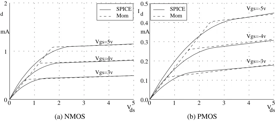
In exchange for its simplicity, the Level-1 piecewise linear MOS model loses the ability to duplicate the behavior of a SPICE model over any arbitrary operating range. However, digital circuits often operate their transistors in particular regions. If the parameters of a piecewise linear transistor are chosen based upon the circuit in which it is used, good results can be obtained.
CMOS gates
For static CMOS gates, the parameters should be chosen to match the I-V characteristics of the SPICE model in a region of greatest current, that is, 2
:
5< V
gs<
5 and 2:
5< V
ds<
5. The rationale is that typically most of the change in voltage at the output of a CMOS gate occurs with the output transistors biased into their high current range. Because the rate of change of voltage is proportional to the current, modeling errors in regions of low current usually produce smaller timing errors than errors in regions of high current. Figures 20 and 21 illustrate the ability of the piecewise linear models to match the I-V characteristics ofds
0 1 2 3 4 5
V 0.0
0.2 0.4 0.6 0.8 1.0
mA
I d
Mom SPICE Vgs=5v
Vgs=4v
Vgs=3v
ds
0 1 2 3 4 5
V 0.0
0.1 0.2 0.3 0.4 0.5
mA
I
d Mom
SPICE
Vgs=-5v
Vgs=-4v
Vgs=-3v
(a) NMOS (b) PMOS
Figure 20: Piecewise Linear vs SPICE I-V Characteristics:
V
gs = 3,4, and 5 volts, SPICE Level-2 models for MOSIS 2Process.ds
0 1 2 3 4 5
V 0
1 2
mA
Mom SPICE I
d
Vgs=5v
Vgs=4v
Vgs=3v
ds
0 1 2 3 4 5
V 0.0
0.1 0.2 0.3 0.4 0.5
mA
I
d Mom
SPICE Vgs=-5v
Vgs=-4v
Vgs=-3v
[image:45.612.106.561.122.323.2](a) NMOS (b) PMOS
Figure 21: Piecewise Linear vs SPICE I-V Characteristics: SPICE Level-3 models for MOSIS 1
:
2Process.In these figures, the I-V curves of the piecewise linear models are superimposed over those of the SPICE models that they were tailored to match. The figures reveal a very good match in the saturation region for large values of
V
gsandV
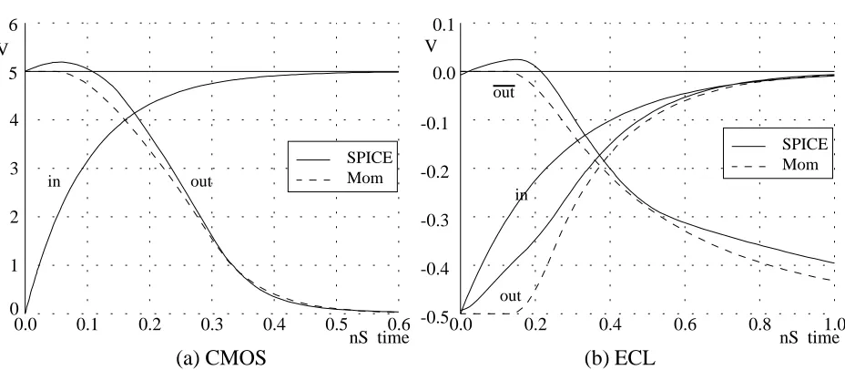
ds.The quality of the match is also born out by a comparison of the transient responses of CMOS inverters (Figure 22) using SPICE vs piecewise linear transistors.7 Figure 23
in out
Figure 22: CMOS Inverter
shows the responses for fast and slow rising exponential inputs. However, the match of I-V characteristics is not as good for lower values of
V
gs. Figure 24 plotsI
d vsV
gs and shows7In this section only the modeling of transistor I-V characteristics is considered. The modeling of nonlinear
time
0 10 20
nS 0
1 2 3 4 5 V
in out
Mom SPICE
time
0 10 20
nS 0
1 2 3 4 5 V
Mom SPICE
in out
Figure 23: Inverters Using Piecewise Linear vs SPICE Transistors.
gs
0 1 2 3 4 5
V 0.0
0.2 0.4 0.6 0.8 1.0
mA I
d MomSPICE