Published online January 13, 2015 (http://www.sciencepublishinggroup.com/j/jeee) doi: 10.11648/j.jeee.20140206.11
ISSN: 2329-1613 (Print); ISSN: 2329-1605 (Online)
New Delta Sigma modulator structure using second order
filter in one stage technique
M. Dashtbayazi
1, M. Sabaghi
2, *, M. Rezaei
3, S. Marjani
11
Department of Electrical Engineering, Ferdowsi University of Mashhad, Mashhad, Iran
2
Laser and Optics Research School, Nuclear Science and Technology Research Institute (NSTRI), Tehran, Iran
3
Department of Electrical Engineering and Computer Engineering, Laval University, Quebec City, QC, Canada
Email address:
[email protected] (M. Sabaghi)
To cite this article:
M. Dashtbayazi, M. Sabaghi, M. Rezaei, S. Marjani. New Delta Sigma Modulator Structure Using Second Order Filter in One Stage Technique. Journal of Electrical and Electronic Engineering. Vol. 2, No. 6, 2014, pp. 82-88. doi: 10.11648/j.jeee.20140206.11
Abstract:
In this paper, a new structure of delta sigma modulator has been proposed in which a second order filter in one stage technique has been taken into the account and a second order noise shaping method and a third order one have been designed by the proposed idea. In the proposed structure an OPAMP has been saved and since in a conventional delta sigma modulator OPAMPs consumes most of the power and takes very large area, the proposed idea causes less power consumption and also the chip area is minimized.Keywords:
Delta Sigma Modulator, Noise Shaping, Second Order Filter in One Stage Technique1. Introduction
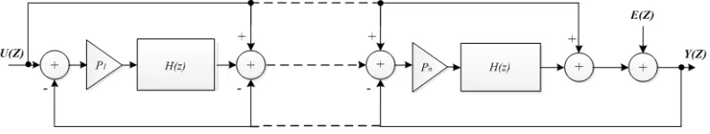
Delta sigma modulators are categorized in communicational modulators. It has been widely used in Transceivers [1]. It has also many applications in signal processing [2]-[3]. In fact these modulators convert analog input signal U(z) to a digital representation Y(z). The difference between output digital signal and input analog signal of modulators is so called quantization error E(z). Quantization error is known as noise which limits analog to digital modulators accuracy. In this type of modulators, the
quantization noise is fed back to the input of the modulator and being attenuated while passing through loop filters. In addition, any other noise sources which are located in the forward path of the modulator could be attenuated by this technique of fed back the noise signals to the input. Attenuating quantization noise causes an increase in accuracy of the modulator. Concept of a conventional delta sigma modulator is shown in figure 1.
Fig. 1. The conventional delta sigma modulator.
The signal transfer function STF(z) and noise transfer function NTF(z) of the delta sigma modulator is as the following:
= 1 − + (1)
= = 1
= = 1 − (2)
provide the same noise transfer function and signal transfer function as the conventional has for the high order noise shaping by mathematical techniques [5][6][7].
In this paper, a new mathematical technique has been introduced in which provides a second order noise shaping and third order noise shaping by a second order filter in one stage technique.
The paper has been organized as the following. Sections II and III describe the proposed second order noise shaping method and results. It has been followed by the proposed third order noise shaping method and its results in sections IV and V. Finally, the paper presents the conclusion.
2. Proposed Second Order Noise Shaping
Method
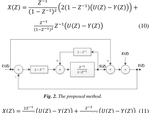
A second order noise shaping is possible even in one filter. The proposed method presents a system in which one filter block can provide a second order noise shaping. The proposed technique is depicted in figure 2. In the proposed method one OPAMP is enough to provide a second order noise shaping. In fact, instead of using two OPAMPs only one OPAMP will be used. Since power consumption of a delta sigma modulator is highly related to power consumption of its OPAMPs, saving an OPAMP means saving half of the power approximately. Furthermore, removing an OPAMP means smaller chip area.
In the figure 2 the signal X(z) is being calculated by:
= 1 − + 2 − − (3)
Obviously, this equation could be simplified in the way that collecting X(z) in left side and the other parameters in the right side of the equation.
1 − = 2 − − (4)
= 2 − − (5)
= 2 − − (6)
1 − = 2 − − (7)
Then, (1-Z-1) could be moved from left side to the right
side of the equation.
= 2 − − (8)
Also (2-Z-1) in the right side of the equation could be
rewritten as (2-Z-1+Z-1-Z-1), so the equation (8) turns to:
= 2 − 2 + − (9)
= 1 − !2 1 − − " +
− (10)
Fig. 2. The proposed method.
= − + − (11)
Furthermore, digital output signal Y(z) is being calculated by:
= + +1 −2 − +
− (12)
All the Y(z) parameters could be collected in the left side of the equation and other parameters in the right side.
#1 +1 −2 + 1 − $ =
1 + + + (13)
Then, the equation (13) could be simplified as:
#1 − + 21 − 1 − + $ =
! % % " + (14)
#1 − 2 + 1 −+ 2 − 2 + $ =
! % % % " + (15)
! " = ! " + (16)
Finally the output signal is simplified as:
= + 1 − (17)
Fig. 3. Ideal implementation of the proposed method.
Fig. 4. Actual implementation of the proposed method.
3. Simulation Results of the Proposed
Second Order Delta Sigma Modulator
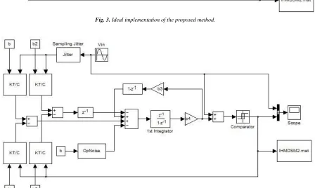
MATLAB implementation of the proposed method is shown in figure 3. Obviously only one integrator has been located in the forward path and a second order filter technique has been taken into the account to perform a second order noise shaping.
Considering actual effects in implementation of this method leads to the MATLAB circuit diagram is shown in figure 4. In this figure, sampling jitter, thermal noise of switched capacitors and OPAMP noise have been taken into the account as presented in [5].
To simulate MATLAB models presented in Figure 3 and 4 all the parameters are considered as the parameters presented in table 1.
The Power Spectral Density (PSD) of the proposed second order noise shaping method is shown in figure 5. Also, the comparison between the actual implementation and the ideal implementation method has been shown in the figure 5.
Table 1. Simulating parameters are used to simulate the proposed idea
(second order delta sigma modulator).
Value Parameter
fBW=100Hz
Signal bandwidth
FS= 50kHz
Sampling Frequency
OSR=250 Oversampling ratio
N=65536 Number of Samples
b=2,b2=b3=1 Ideal Delta-Sigma Coefficient
b=0.5,b2=0.25,b3=b4=1 Actual Delta-Sigma Coefficient
Another simulation result in which Signal to Noise and Distortion Ratio (SNDR) has been plotted versus input analog signal amplitude has been depicted in figure 6 and figure 7. In figure 6, variation of SNDR versus input amplitude has been studied by different sampling jitters. And in figure 7, variation of this parameter has been studied by different OPAMP saturation levels.
Comparison between the result obtained from the proposed method and ideas presented in [5], [6], [7] and [8] has been presented in table 2.
Table 2. Comparison between related works and the proposed idea.
This Work [8]
[7] [6] [5] Parameters
100 500 10k 256 100 fBW(Hz)
2 2 2 2 2 Order
91.6 76
87.8 72
90.2 SNDR(dB)
14.9 12.3 14.3 11.7 14.7 ENOB1(bit)
1 Effective number of bits [4]
Fig. 5. The PSD diagram of the proposed second order noise shaping
method.
4. Proposed Third Order Noise Shaping
Method
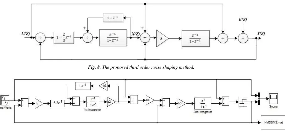
It is also possible to extend this idea for third order noise shaping. The proposed technique for third order noise shaping is shown in figure 8. In this idea also an OPAMP has
been saved and power consumption and chip area will be minimized.
Fig. 6. SNDR versus analog input amplitude per different sampling jitters.
Fig. 7. SNDR versus analog input amplitude per different OPAMP saturation
levels.
Fig. 8. The proposed third order noise shaping method.
In the figure 8 the signal X(z) is being calculated by:
= 1 − + !1 −& " − (18)
Collecting all X(z) in the left side of equation gives:
1 − = !1 −& " − (19)
= 1 −& − (20)
= 1 −& − (21)
Simplifying equation (21) gives:
1 − = 1 −& − (22)
Moving (1-Z-1) from left side of the equation 22 leads to:
= 1 −& − (23)
Also the output signal Y(z) could be calculated as:
= + + & − + (24)
Replacing X(z) from (24) by equation (23) gives:
= + +1 −3 − +
1 −& − (25)
Replacing (1-2/3Z-1) by (1-Z-1+1/3Z-1) gives:
= + +1 −3 − +
1 − +& − (26)
= + +1 −3 − +
&
− + ( ( − (27)
Collecting all Y(z) to the left side and the others to the right side gives:
#1 +1 −3 + 1 −3 + 1 − & &$ =
1 + & + & + ( ( + (28)
Simplifying equation (28) leads to:
! & %& (%& ) (%& (%& & (% (" =
! & %& (%& ) (%& (%& & (% (" +
(29)
! (" = ! (" + (30)
Finally moving (1-Z-1)3 from left side of the equation to the right side gives:
= + 1 − & (31)
The equation (31) is output signal of a third order noise shaping delta sigma modulator.
5. Simulation Results the Proposed Third
Order Delta Sigma Modulator
Ideal MATLAB model of the proposed third order noise shaping method has been shown in the figure 9. If noise sources such as thermal noise from switched capacitors, sampling jitter and OPAMP noise being considered, a model such as what is shown in figure 10 will be reached.
To simulate MATLAB models presented in Figure 9 and 10 all the parameters are considered as the parameters presented in table 3.
Table 3. Simulating parameters are used to simulate the proposed idea (third
order delta sigma modulator).
Value Parameter
fBW=300
Signal bandwidth
FS= 50kHz
Sampling Frequency
OSR=83.3 Oversampling ratio
N=65536 Number of Samples
b=b4=0.33,b2=b3=1,b5=3 Ideal Delta-Sigma Coefficient
b=3/7,b2=2/7,b3=b4=b5=b7=1,b6=0.5,b 8=1.5
Actual Delta-Sigma Coefficient
The PSD diagram of the proposed third order noise shaping method and comparison between the actual implementation and the ideal implementation method have been shown in figure 11.
Fig. 11. The PSD diagram of the proposed third order noise shaping method.
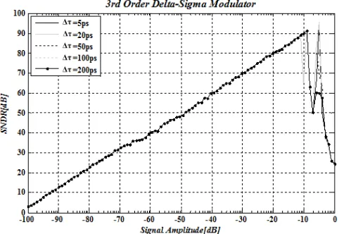
Same as simulation results for the proposed second order noise shaping, simulation results in which SNDR versus analog input signal amplitude has been depicted in figure12 and figure 13. In figure 12, variation of SNDR is studied by different input sampling jitters. And figure 13 shows this parameter versus different OPAMP saturation levels.
Fig. 12. SNDR versus analog input amplitude per different sampling jitters.
Fig. 13. SNDR versus analog input amplitude per different sampling jitters.
Obviously, same as the results obtained from the proposed second order noise shaping idea, maximum SNDR has been reached in -8db for the input analog signal amplitude.
Comparison between the result obtained from the proposed method and ideas presented in [9], [10] and [11] has been presented in table 4.
Table 4. Comparison between related works and the proposed idea.
This Work [11] [10] [9] [9] Parameters 300 100k 20k 20k 120 fBW(Hz)
3 3 3 3 3 Order 91.5 84 61.4 81 65 SNDR(dB) 14.9 13.7 9.9 13.2 10.5 ENOB(bit)
6. Conclusion
In this paper a method has been proposed in which an OPAMP has been saved compared with conventional delta sigma modulator and still the functionality of the delta sigma modulator is correct. Removing one OPAMP leaded to smaller chip area and less power consumption. The proposed idea has been studied in second order noise shaping and third order noise shaping delta sigma modulator. Also the comparison between the proposed idea and other techniques shows better SNDR and effective number of bits.
References
[1] L. Bos, G. Vandersteen, P. Rombouts, A. Geis, A. Morgado, Y. Rolain, G.V. Plas and J. Ryckaert, “Multirate cascaded discrete-time low-pass ∆Σ modulator for GSM/Bluetooth/UMTS,” IEEE J. Solid-State Circuits, vol. 45, pp. 1198-1208, June 2010.
[2] L. Yao, M. S. J. Steyaert, and W. Sansen, “A 1-V 140-µW 88-dB audio sigma-delta modulator in 90-nm CMOS,” IEEE J.
Solid-State Circuits, vol. 39, pp. 1809-1818, Nov. 2004.
[3] E. Fogleman, J. Welz, and I. Galton, “An audio ADC delta-sigma modulator with 100-dB peak SINAD and 102-dB DR using a second order mismatch-shaping DAC,” IEEE J.
[4] D. Johns and K. Martin, Analog Integrated Circuit Design. New York: Wiley, 1997.
[5] P. Malcovati, et al., “Behavioral modeling of switched-capacitor sigma-delta modulators,” in IEEE Trans. Circuits
Syst. I, vol. 50, pp. 352 - 364, Mar 2003.
[6] F. Cannillo, et al., “ 1.4 V 13 W83dBDRCT- modulator with dual-slope quantizer and PWM DAC for bio potential signal acquisition,” in Proc. ESSCIRC, pp. 267-270, Sept. 2011. [7] A. Nilchi and D. A. Johns, “A low-power Delta-Sigma
modulator is using a charge-pump integrator,” in IEEE Trans.
Circuits Syst. I, vol.60, pp.1310-1321, May 2013.
[8] A.F. Yeknami, et al., “Low-Power DT ∆Σ Modulators Using
SC Passive Filters in 65 nm CMOS,” in IEEE Trans. Circuits
Syst. I, vol.61, pp.358-370, Feb. 2014.
[9] Y. Chae and G. Han, “Low voltage, low power, inverter-based switched-capacitor Delta-Sigma modulator,” in IEEE J.
Solid-State Circuits, vol. 44, pp. 458-472, Feb. 2009.
[10] F. Michel and M. Steyaert, “ A 250 mV 7.5 W 61 dB SNDR SC modulator using near threshold voltage biased inverter amplifiers in 130 nm CMOS ” in IEEE J. Solid-State Circuits, vol. 47,pp.709-721, May 2012.
[11] A.P. Perez, E. Bonizzoni and F. Maloberti, “A84dB SNDR 100 kHz Bandwidth Low Power Single Op-Amp Third-Order ∆Σ Modulator Consuming 140µW,” in IEEEISSCC Dig. Tech.