Copyright © 2014 IJECCE, All right reserved
Discrete Time Sigma-Delta Modulator with the
Objective of Power Consumption Reduction with 130 um
Technology
Rouzbeh Jahani
Deptt. of Computer Engg., Shahindezh Branch, Islamic Azad University, Shahindezh, Iran
Email: [email protected]
Heidar Ali Shayanfar
Department of Electrical
Engineering, South Tehran
Branch, Islamic Azad
University, Tehran, Iran
Alireza Gharegozi
Department of Computer Engineering, Shahindezh
Branch, Islamic Azad University, Shahindezh, Iran
Mohsen Tamaddon
Department of Computer Engineering, Shahindezh
Branch, Islamic Azad University, Shahindezh, Iran
Abstract – In this paper a mono-loop discrete time sigma-delta modulator of order 2 is designed and implemented. The major aim of the design is to decrease the power consumption. To attain this goal this paper attempts to optimize the high power characteristic of the OTA modulators. Using an appropriate design and taking the power of biasing sources into account, the amplifier expends 1 mw for operation. At first, this modulator is simulated using MATLAB software as a system which encounters various conditions. The blocks of this modulator, in circuit level, are simulated with ADS software. The operational frequency of this modulator is 12 KHz whose ultra sampling rate is 256 for SNR˃85dB.
Keywords – Sigma-Delta Modulator, OTA Modulators, ADS Software.
I.
I
NTRODUCTIONSigma-delta modulator is a conventional method on which comprehensive examinations are made to convert an analogue signal to very high frequency digital series (J. C. Candy and G. C. Temes, 1992), (S. R. Northworthy, et. al., 1997). Among the major characteristics of sigma-delta modulatorsare: 1. A sampling rate more than nyquist rate, 2. Can use low resolution quantizers. 3. Energy of the noise in quantizer range of performance is removed from. Moreover, the sigma-delta modulators have the least sensitivity to the non-ideal characteristics of analogue elements. Therefore, it is the best option for high resolution applications like digital voice. Up to now, many delta-sigma-based modulators have been designed. However, most of these methods use 0.35 um technology with the power source amplitude of more than 3 volt. In this study the 0.13um technology with voltage source of 1.2v is used for the purpose of a low power circuit in conjunction with the low-power low-voltage digital auxiliary apparatus. To achieve this goal, and streamline the complexity of the design and also to warrant the stability, the modulator’s structure is selected in form of a 2-order mono-loop structure in which the capacitor switching technique is utilized. The structure provides the discrete time calculation, low complexity and low power consumption. In first section, the simulation of different system conditions and feedback coefficient is performed via MATLAB software. Modulator design and simulation results are brought in next section. At the end, the total power consumption of the sigma-delta modulator of order 2 will be calculated. The ADS software is used for simulations.
II.
D
ESIGNI
NS
YSTEML
EVEL
Modulator's structure
Fig. 1 depicts a mono-polar sigma-delta Ideal modulator is calculated by Eq. 1. The OSR is ultra sampling rate and b indicates what bit-number the equalizer is. In this study b takes 1.
𝑆𝑁𝑅𝑝𝑒𝑎𝑘 =
3𝜋 2 2
𝑏− 1 2𝑛 + 1 (𝑂𝑆𝑅
𝜋 )
2𝑛+1 (1)
The primary issue of a multi bit sigma-delta is the linearity of equalizer. Therefore, in system part, the modulator is simulated for multi bit states. For the purpose of a better comparison, From Eq.1 for a 16-bit resolution the OSR (which OSR =fs/2fin) should be taken 256. It should be noted that for implementation of decimation filter, the OSR should be dyadic. By considering OSR=256 for a 1-bit modulator, the SNR is 19 dB. On this basis, the maximum SNR approximately yields a 17-bit resolution.
III.
D
ESIGN INC
IRCUITL
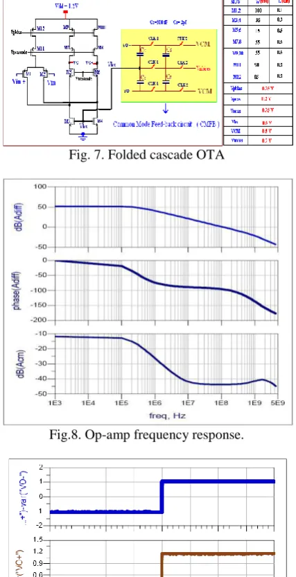
EVELFig.7 shows a differential tilted op-amp. The differential structures can achieve the gain, bandwidth as well as swing amplitude more than a mono-output amplifier could achieve. The use of PMOS inputs can remove the presence of chopper stabilization for less flicker noise than the NMOS type transistors (Mohammad Yavari and Omid Shoaei). One of the primary issues of nanometer technologies like 13nm technology is the small output impedance of the transistors. Therefore, applying them for higher gains is one of the major limitations of this technology. Taking the biasing sources into account, the provided gain-curve shows a gain about 52 dB and the CMRR= 63 dB as well as power consumption=1watt. In order to warrant the common mode voltage in fully differential amplifier, a CMFB circuit is considered in terms of a capacitor switch analogue to digital converter.
1 2
1 2
3 4 2 3 5 3 4
(1 )
( ) (3)
1 ( 2) (1 )
z Ntf z
z a a a a a z a a
relatively great noise (like Quintet noise) attenuated, this drawback could be attenuated as well. Totally, the critical challenge of the modulator design in circuit level relates to the first block. To realize this comparator, a structure called open surviving latch is used (see fig. 12)
Transistors M2,3 and M8,9 which are coupled in diagonal topology, are triggered by signal inserted to the drain instead of the source. In this way the block gating effect could be removed and the surviving rate could be promoted.
Watch generator circuit
A capacitor switch integrator needs 4 clocks (pulses) to operate appropriately; two signals have delayed to one another and the rest two signals are in non-overlapped form. Figure 19 shows the generation of these 4 signals. The delayed pulses are used to decrease the load discharge related to the input signal when the transistors are off.
Modulator circuit schematic
The 2-order modulator is appropriate for a 16-bit resolution. However, in high resolution modulators, the sampling capacitor value is determined by KT/C; the switching related noise. For fully differential modulator, by considering the switching noise, the SNR is:
𝑆𝑁𝑅𝐾𝑇
𝐶 =
(2×𝑂𝐿×𝑉𝑟𝑒𝑓)2
2 ×
𝐶𝑠×𝑂𝑆𝑅
4𝐾𝑇 (2) Holding C3= 1pf, the SNR calculated by E.q 2 is 106 dB. This value meets the 16-bit resolution. The following diagrams indicates the simulation results.
2-order sigma-delta modulator with coefficients a1 to a5 is:
Fig.1. 1-bit modulator
Fig.2. Order delta-sigma modulator
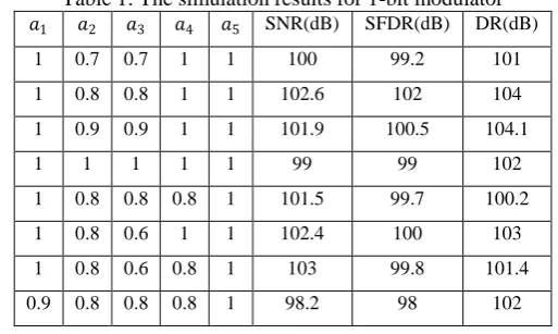
The system simulation results for different values of modulator coefficient are shown in table1. From table 1, the best case of the modulator parameters occurs when a1=0.8 and a2=0.8 while the rests take 1. The SNR value
of this case is 102.6 dB. As regards 2-bit modulators, the values increase by 2-3dB. The increment calculated by Eg. 1 takes 3.7 dB.
Fig.2 presents the SNR diagram for 3 different input values. As shown, the SNR value gets the maximum value for a2=a3=0.8. Out of the 3 cases, the efficient bit value or ENOB can be calculated by:
)
1
(
@
15
.
16
)
7
.
0
(
@
3
.
16
)
8
.
0
(
@
75
.
16
)
5
(
02
.
6
76
.
1
3 2 3 2 3 2
a
a
ENOB
a
a
ENOB
a
a
ENOB
SNR
ENOB
Fig. 16 depicts the schematic of the 2-order mono-loop discrete time modulator. The modulator is controlled by a clock generator. To decrease the changes in samples and the short circuit resistance of the switches and to increase the linearity of the switches, all switches supposed to be CMOS type. One of the advantages of the capacitor-switch ADC circuits is that they don’t need the S&H circuits. The S&H circuits pose a critical challenge in ADC design either for their high power consumption or for their complex designs. Invoking the presence of S&H circuits the complexity gets decreased and the major reduction in power consumption is yielded.
Power consumption calculation
In order to calculate the total power consumption of the modulator, power of each block is calculated and eventually all powers are aggregated. However, with the exclusion of op-amp circuits, all blocks consume dynamic power and with no clock the power consumption would be little and negligible.
256, in 10 , sw 5.12 , dd 1.2 , L 1
OSR f kHz f MHz V V C pf
2 0
.
. . .
2 32 1 2 2.5
OTA d dd
dynamic L dd sw
total OTA switch comparator DAC
p I V
p C V f
P P P P P mW
IV.
C
ONCLUSION(I)
In this work a 2-order mono-loop delta-sigma modulator is simulated in discrete time domain. This method yields the SNR=95dB. The modulator blocks are also simulated in circuit level considering 0.13um technology. It was shown that the total power = 2.5w.
Table 1: The simulation results for 1-bit modulator
𝑎1 𝑎2 𝑎3 𝑎4 𝑎5 SNR(dB) SFDR(dB) DR(dB)
1 0.7 0.7 1 1 100 99.2 101
1 0.8 0.8 1 1 102.6 102 104
1 0.9 0.9 1 1 101.9 100.5 104.1
1 1 1 1 1 99 99 102
1 0.8 0.8 0.8 1 101.5 99.7 100.2
1 0.8 0.6 1 1 102.4 100 103
1 0.8 0.6 0.8 1 103 99.8 101.4
Copyright © 2014 IJECCE, All right reserved Fig.3. and Fig.4. 2-bit modulator' PSD output of 2-bit
modulator
Fig.5. SNR Value
Power consumption calculation
In order to calculate the total power consumption of the modulator, power of each block is calculated and eventually all powers are aggregated. However, with the exclusion of op-amp circuits, all blocks consume dynamic power and with no clock the power consumption would be little and negligible.
P
P
P
P
mWP
f V C p
V I p
pf C V V MHz f
kHz f OSR
DAC comparator switch
OTA total
sw dd L dynamic
dd d OTA
L dd
sw in
5 . 2 2 1
32 2
. . . .
1 , 2 . 1 , 12 . 5 , 10 , 256
2 0
V.
C
ONCLUSION(II)
In this work a 2-order mono-loop delta-sigma modulator
is simulated in discrete time domain. This method yields the SNR=95dB. The modulator blocks are also simulated in circuit level considering 0.13um technology. It was shown that the total power = 2.5w.
Circuits' figure_ diagrams and tables simulated by ADS
Fig.6 . The 2-order mono-loop discrete time modulator
Fig. 7. Folded cascade OTA
Fig.9. Off-set voltage of op-amp (micro volt) Vos=10uv
Fig.10. The output curve of op-amp in time domain and the CMFB effect in output voltage
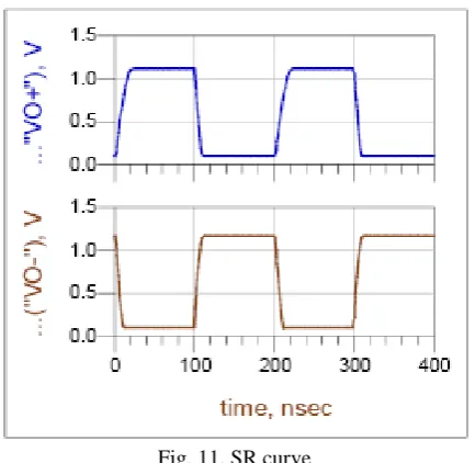
Fig. 11. SR curve
Figures associated with the comparator
Fig.12. 1-bit comparator circuit
Fig.13. The time domain output for 2 sinusoidal inputs
Fig.14. The minimum voltage difference between two inputs for toggling the output Vdiff(min)=0.45V
Figures associated with the 1-bit ADC
Copyright © 2014 IJECCE, All right reserved Fig.16. Input and output
Figures associated with the capacitor switch based
integrator
Fig.17. Capacitor switch- based integrator
Fig.18. Integrator-made difference phase for sinusoidal input. 253 This difference is about 90 deg. For the
frequency=10KHz
Figures associated with the clock generator
Fig.19. clock generator circuit
Fig.20. The curves generated by clock generator circuit( T-delay 10 nsec)
R
EFERENCES[1] J. C. Candy and G. C. Temes, “Oversampling Delta-Sigma Data
Converters,” Piscataway, NJ: IEEEPress, 1992, ISBN
0-87942-285-8.
[2] S. R. Northworthy, R. Schreier, and G. C. Temes, “Delta-Sigma
Data Converters,” Piscataway, NJ: IEEE Press, 1997, ISBN 0-7803-1045-4.
[3] Mohammad Yavari and Omid Shoaei,”A 3.3V Second-Order
Sigma-Delta Modulator for Digital Audio,” Electrical & Computer Engineering Department, University of Tehran, Iran
[4] Shahriar Rabii and Bruce A. Wooley,”A 1.8-V Digital-Audio
Sigma-Delta Modulatorin 0.8-m CMOS,” Stanford University. Stanford, CA 94305
[5] Sumith kumar Nathany ,”14- bit Fully differential discrete time
sigma-delta modulator,”A Thesis for the Degree of master of
science Department Of Electrical Engineering KATE
GLEASON College Of Engineering. Rochester Institute Of Technology .ROCHESTER, NEW YORKNOVEMBER 2006
[6] Syam Prasad SBS Kommana,”first order sigma-delta modulator
of an oversampling ADC in CMOS ,using floating gate mosfets,”
A Thesis Submitted to the Graduate Faculty of theLouisiana State University and Agricultural and Mechanical College in partial fulfillment of therequirements for the degree of Master of Science in Electrical Engineering. Bachelor of Technology, Nagarjuna University, 2001 December 2004
[7] Brian P.Brandt, drew E.Wingard ,Bruce A.Wooley ,”Second
Order Sigma-Delta Modulation For Digital-Audio Signal Acquisition,” IEEE JOURNAL OF SOLID STATE CIRCUITS,
26(4), APRIL 1991.
[8] David A. Sobel “A 25 Ms/s Nyquist-Rate Sigma-Delta