NANOTECHNOLOGY IMPACT ON INFORMATION TECHNOLOGY
Gaurav Kumar*
Vasudha Rani**
INTRODUCTION
Research on the nanoscale has led to the development of completely novel materials that will
undoubtedly find numerous applications. The integrated circuit which, during recent years
has become the basis of modern digital electronics functions by making use of electron range.
However, electronics also possess the quantum mechanical property of spin, which is
responsible for magnetism. New “spintronic’ technologies seek to make use of this electron
spin. Some time in conjunction with electron charge, in order to achieve new types of
devices. Several spintronic devices are currently being developed that outperform traditional
electronics. Often this results from an increased functionality, which means that a single
spintronic element performs an operation that requires several electronic elements. Different
approaches to spintronics have been developed by semiconductor and magnetism properties.
Although there have been some very impressive demonstrations of spin polarized charge
transport and ferromagnetism in cooled semiconductors, the lack of reliable room
temperature semiconductor ferromagnet has hampered their applications. Within the
magnetism community considerable success has been achieved at room temperature by using
common ferromagnetic materials such as Ni81Fe19. This approach offers the benefit of low
power operation, non-volatile data storage and a high tolerance of both impurities and
radiation.
A great success of electronics has been the ability to use group of transistors for performing
the Boolean logic operations. Magnetic logic seeks to perform the necessary for a logic
system with ferromagnetic metals to make use of advantages that these materials offer. One
approach has been to use magnetic/non-magnetic/magnetic tri-layer structures known as
magnetic tunnel junctions (MTs). These have an electrical resistance that depends on the
relative orientation of magnetization of the two magnetic layers, and are commonly used in
magnetic random access memory (MRAM) logic gates made from MTs can perform logic
operations such as AND, OR, NAND, NOR, XOR. Alternatively, MTs may be used to
provide a switchable bias to CMOS transistors so that a logic gate may be capable of
performing one of two logic operations, say logical AND and OR as desired.
*Assistant Professor, Department of Applied Electronics & Instrumentation, JMIT Radaur.
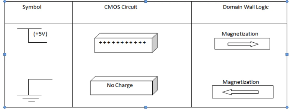
PROPAGATING DATA
Circuits made from planar magnetic nanowires can be used, with wires typically 100 to
250nm wide and 5 to 10 nm thick. The shape anisotropy of these wires creates a magnetic
easy axis in the long axis direction that defines the stable orientation of magnetization as
shown in figure 1. The system with two opposite stable magnetization orientations is ideal for
representing logical “1” and “0”. Where opposite magnetization rotates by 1800(figure 1).
This is another form of magnetic solition and is called domain wall. For the wire dimensions
relevant here, domain walls are typically approximately 100nm wide. Domain walls can be
moved by applying magnetic fields and it is this ability which is exploited in magnetic
domain wall logic. Domain walls travel down sections of nanowire between nanowire
junctions where logic operations are performed. Crucially, the influence of nanowire
imperfections on domain wall propagation is very significantly reduced compared with the
propagation of solitions in interacting dots. Furthermore very little power is required either to
propagate a domain wall or to perform a logic operation compared to the lowest power
CMOS equivalent or magnetic alternatives. This combination makes magnetic domain wall
logic a robust low power logic technology.
Figure 1: Magnetic Domain Wall Logic
Using a unidirectional field will not allow domain walls to be separated reliably and hence
normal data streams both “1” and “0” cannot be propagated. Instead use is made of the
orthogonal fields to create a magnetic field vector that rotates in the plane of the sample to
control domain wall propagation around smooth 900 wire corners. An important rule for
understanding the nanowire circuits is that domain walls will propagate around the corners of
the same sense of rotation as the applied field- that is a clockwise rotating field will lead to
domain walls travelling around corners clockwise. In a correctly designed nanowire circuit
the sense of field rotation will define a unique direction of domain wall propagation and
direction of data flow in magnetic domain wall logic can in principle be reversed simply by
reversing the sense of filed rotation.
DATA PROCESSING
The NOT gate was the first domain wall logic device to be introduced [1-3] and is foundational
to the development of all other logic elements figure 2 shows the geometry of a NOT gate
and illustrates its principle of operation. The NOT gate is a junction formed by two wires. For
a given field rotation one wire will act as the input and other wire as output. A small central
“stub” which emerges from the wire junction is an important part of the device as it ensures
there is sufficient shape anisotropy to maintain a magnetization component in direction in
which the stub points. Under a rotating magnetic field H a domain wall enters the NOT gate
input before reaching the wire junctions. The magnetization following the domain wall points
in the direction of domain wall propagation. Provided that there is sufficient field the domain
wall expands over the junction and splits in two, with one domain wall travelling along the
central stub, leaving the stub magnetization reversed and the other free to propagate on the
NOT gate output wire (figure 2). As the field continues to rotate the domain wall in the
output wire leaves the NOT gate.
Figure 2: Diagrams showing the operating principle of NOT gate. The arrows
represents instantaneous magnetic field vector, while the arrows inside show’s the
wire’s internal magnetization configuration.
The magnetization following the domain wall is now pointing away from the direction of
domain wall motion. The magnetization on either state of the wire junction is reversed and
the device has inverted the input logic state. The reversal in magnetization means that the
inversion process would be expected to require a one half cycle of field. The other circuit
elements that are required for realistic logic system are a minority gate, signal fan out and
signal cross over. The NOT gate operating phase provides a useful and necessary reference
for comparing the performance of these additional elements to ensure compatibility.
Domain walls were introduced to nanowire junctions either by using topological constraints
of a nanowire circuit or a domain wall injection form a large area pad. These are both valid
method for developing logic elements, although a method of entering user defined data is still
required to create viable logic system. An element for data input is presented that is
integrated with domain wall shift register [4]. The design of the optimized data input element
is obtained from a simple test structures, overlaid with that of a NOT gate. A single phase
boundary for the data input element bisects the NOT gate field operation area. Above the
phase boundary no magnetic reversal occurs. Two sets of field amplitude can then be
indentified for operating both NOT gates and the data input element. Below the data input
element phase boundary are the read or no write field conditions above the phase boundary
are the write field conditions.
Figure 3 shows an image of a shift register containing eight NOT gates and one Fan out
junction [4]. In addition, one NOT gate has a data input element attached to its central stub.
The fan out element provides a monitor arm for measurement. The shift register can be
divided into ten cells, each capable of holding a single domain wall and separated from its
neighbor by a total of 180o of wire turn. Due to topological restrictions domain walls can only
be introduced or removed into pairs, so a shift register in figure contains five data bits.
Figure 3: FIB image of a continuous shift register made of eight NOT gate.
MEMORY WITH MEMRISTOR
Nanowires coated with titanium dioxide can be used as memory devices. One group of these
nanowires is deposited parallel to another group. When a perpendicular nanowire is laid over
a group of parallel wires, a device called a memristor is formed at each intersection. A
memristor can be used as a single-component memory cell in an integrated circuit. By
reducing the diameter of the nanowires, researchers believe memristor memory chips can
NANOWIRE RACE TRACKS
Magnetic nanowires made of an alloy of iron and nickel are being used to create dense
memory devices. A method is used to magnetize sections of these nanowires. By applying a
current the magnetized sections can move along the length of the wire. As the magnetized
sections move along the wire, the data is read by a stationary sensor. This method is called
race track memory because the data races by the stationary sensor. Growing millions of
U-shaped race track nanowires on a silicon substrate to create low-cost, high-density and highly
reliable memory chips.
SILICON DIOXIDE MEMORY SANDWICHES
It is found that silicon dioxide nanowires can used to create memory devices. The nanowire is
sandwiched between two electrodes. By applying a voltage, you change the resistance of the
nanowire at that location. Each location where the nanowire sits between two electrodes
becomes a memory cell. The key to this approach is that we can repeatedly change the state
of each memory cell between conductive and nonconductive without damaging the material’s
characteristics. This is believed that we can achieve high memory densities by using
nanowires with a diameter of about 5 nm and by stacking multiple layers of arrays of these
nanowires like a triple-decker club sandwich.
NANODOTS TO STORE MORE DATA IN SMALLER SPACE
A method is developed to increase the density of memory devices to store information on
magnetic nanoparticles. Growing the arrays of magnetic nanoparticles called nanodots which
are about 6 nm in diameter. Each dot would contain information determined by whether or
not they are magnetized. Using billions of these 6-nm diameter dots in a memory device
could increase memory density.
Figure 4: High-resolution image of a polymer-silicate nanocomposite. This material has
improved thermal, mechanical, and barrier properties and can be used in food and
beverage containers, fuel storage tanks for aircraft and automobiles, and in aerospace
BENEFITS
Nanotechnology is already in use in many computing, communications, and other electronics
applications to provide faster, smaller, and more portable systems that can manage and store
larger and larger amounts of information. These continuously evolving applications include:
• Nanoscale transistors that are faster, more powerful, and increasingly energy-efficient,
soon your computer’s entire memory may be stored on a single tiny chip.
• Magnetic random access memory (MRAM) enabled by nanometer‐scale magnetic tunnel
junctions that can quickly and effectively save even encrypted data during a system
shutdown or crash, enable resume‐play features, and gather vehicle accident data.
• Displays for many new TVs, laptop computers, cell phones, digital cameras, and other
devices incorporate nano structured polymer films known as organic light-emitting
diodes, or OLEDs. OLED screens offer brighter images in a flat format, as well as wider
viewing angles, lighter weight, better picture density, lower power consumption, and
longer lifetimes.
• Other computing and electronic products include Flash memory chips for iPod nanos,
ultra responsive hearing aids; antimicrobial/antibacterial coatings on mouse/keyboard/cell
phone casings; conductive inks for printed electronics for RFID/smart cards/smart
packaging; more life-like video games; and flexible displays for e-book readers.
CONCLUSIONS
Domain wall logic is not contender for replacement of CMOS microelectronics. CMOS is a
highly mature technology with many advantages and still has many yes of scaling available to
it. The limited operational speed of domain wall logic does not render it suitable for many
applications. A strong trend in electronics which is expected to apply to the relationship
between CMOS and too many other areas of nanotechnology in future is to combine multiple
technologies on a single platform: the system on a chip. To implement an AND gate in
CMOS would take six transistors, but domain wall logic achieves this simply by bringing two
nanowires together. The technical difficulties in stacking devices in to 3D in CMOS are (i)
disturbing the power and clock to everywhere inside the volume of the network,(ii) extracting
the waste heat from the center of the network so that the device does not melt. It is believed
that domain wall logic is an excellent choice of primitive for 3D architectures.
REFERENCES:
1. D.A. Allwood, G Xiong, M.D. Cooke, C.C. Faulkner, D. Atikson, R.P. Cowburn,
2. D.A. Allwood, G Xiong, M.D. Cooke, C.C. Faulkner, D. Atikson, R.P. Cowburn, J.
Applied Physics 2004, 95, 8264
3. X. Zhu, D.A. Allwood, G. Xiong, R.P. Cowburn, P. Grutter, App physics let. 2005,
87, 062503
4. D.A. Allwood, G Xiong, D.Petit, C.C. Faulkner, D. Atikson, R.P. Cowburn, science
2005, 309, 1688

![Figure 3 shows an image of a shift register containing eight NOT gates and one Fan out junction [4]](https://thumb-us.123doks.com/thumbv2/123dok_us/8054534.2132815/4.893.250.648.634.860/figure-shows-image-shift-register-containing-gates-junction.webp)

