Structural, Electronic and Optical Properties of the Al
2O
3Doped SiO
2:
First Principles Calculations
Yong Yang
1, Masae Takahashi
1, Hiroshi Abe
2and Yoshiyuki Kawazoe
11
Institute for Materials Research, Tohoku University, Sendai 980-8577, Japan
2Sekisui Chemical Co., Ltd. and Sekisui Integrated Research Inc., Kyoto 601-8105, Japan
The doping effects of Al2O3on SiO2(-cristobalite) have been studied by first principles calculations, with emphasis on the structural,
electronic and optical properties. Compared to pure SiO2 crystal, the electronic density of states (DOS) of the Al2O3doped SiO2 show
significant changes. The electron energy states corresponding to the newly emerged sharp DOS peaks are found to exhibit localized characteristics, which are mainly attributed to the unsaturatedly bonded 2p orbitals of O atoms in the –[Al-O-Al]– linkages. The optical properties of the Al2O3doped SiO2are studied by calculating the frequency-dependent dielectric functions. The electric dipole moment induced
by the electron states near the top of the valence band is found to have significant effect on the optical absorption spectrum.
[doi:10.2320/matertrans.MB200831]
(Received July 10, 2008; Accepted September 11, 2008; Published October 25, 2008)
Keywords: Al2O3-SiO2, –[Al-O-Al]–, first principles calculations
1. Introduction
Crystalline SiO2 is transparent to visible light, due to the
wide band gap between the valence band and conduction band (e.g., the band gap is10eV for -quartz1)). Similar behavior is observed in amorphous SiO2, which is the main
component of window glasses. With the presence of dopants, people can significantly modify the optical absorption properties of SiO2 in the visible range. One of the most
commonly used methods is the co-doping of Al2O3with rare
earth elements (e.g., Nd, Er) into SiO2, and the doped SiO2
are found to exhibit interesting optical and spectroscopic properties, new absorption peaks are observed in the infrared and visible range.2–4)The Al
2O3dopants have been shown to
play an important role in the geometric distribution of rare earth elements, i.e., to prevent the clustering of the rare earth ions, which in return reform the quality of optical devices.4) Numerous experiments have been carried out to study the oxygen coordination number (OCN) of Al atoms in the SiO2
-based glass and their high temperature melts. Using electron paramagnetic resonance (EPR), people have established that Al atoms are more likely to substitute the Si positions in natural quartz.5–7)A number of experiments have suggested the existence of four-coordinated Al atoms in silica.5–9) Three-coordinated Al in silica fused from quartz has been found in EPR experiments.10) In addition, experimental evidence for higher Al coordination such as five- and six-coordinated Al atoms is also reported in silica-based glasses.11,12)
On the theoretical side, classical molecular dynamics (MD) simulations or ab initio calculations have been performed to study the structural properties of Al2O3doped
silica in recent years.13–15) First principles MD simulations based on density functional theory (DFT) have shown that, the oxygen coordination number (OCN) of Al and Si atoms varies from 3 to 5 in the molten silicates of CaO-Al2O3-SiO2,
and the four-coordinated species are dominant.13)Lægsgaard has studied some possible forms of Al impurities in SiO2
network by DFT calculations, which show that the Al atoms
present as isolated impurities with three or four coordination oxygen atoms at low Al2O3concentrations.14)A recent work
based on classical MD simulations has studied the static and dynamic properties of Al2O3-SiO2 melts, in which the O
coordination numbers of Al and Si are found to depend on the Al2O3 concentration.15)Most of these efforts have been
focused on the structural and dynamical properties of the Al2O3-SiO2glasses or their melts. Contrary to the structural
properties, the changes that Al2O3 bring to the electronic
and optical properties of SiO2, even the simplest case of
crystalline SiO2, are poorly studied at quantum mechanical
level.
In the present work, we aim at exploring the doping effects of Al2O3 on SiO2 crystal, by using density
func-tional theory (DFT) calculations. In spite of the relatively small simulation cell, the Al2O3 doped SiO2 model
employed in our studies has captured the some of the important aspects of the aluminosilicate glasses. The electronic structures of the Al2O3 doped SiO2 (abbreviated
as Al2O3-SiO2) are significantly modified when comparing
to the pure SiO2 crystal, the electronic density of states
(DOS) split into sharp peaks near the top of valence band. The energy states of the sharp DOS peaks are found to bear localized features, which originate from the unsaturatedly bonded 2p orbitals of O atoms in the –[Al-O-Al]– linkages. Some new states are observed to emerge in-between the valence and conduction bands, which can be recognized in the calculated optical absorption spectra. The electric dipole moment induced by the electronic states around the top of valence band is found to have significant influence on the absorption characteristics. To the best of our knowledge, this is the first theoretical report on the electronic density of states near the Fermi level, as well as the optical properties in the Al2O3-SiO2 system.
The contents of this paper are organized as follows: after this introduction part, section 2 describes the computational method and model used in this work. Section 3 presents the results and discussions on the Al2O3 doped SiO2 structures.
A summary of this work is given in section 4.
Special Issue on Advances in Computational Materials Science and Engineering V
2. Computational Method
The DFT calculations were performed by the VASP code,16–19) employing a plane wave basis set and the PAW potentials20,21) to describe the behavior of electrons. The exchange-correlation energies are described by the Perdew-Wang (PW91) functionals with the generalized gradient approximations (GGA).22) The SiO
2 crystal under
consid-eration is the -cristobalite, which also serves as host materials for the Al2O3 dopants. The primitive unit cell of -cristobalite crystal contains 12 atoms: 4 Si and 8 O atoms. The Al2O3-SiO2 structures in our studies are constructed by
replacing some Si atoms in the host lattice of-cristobalite SiO2 with Al atoms and removed the excess Si and O atoms
to get the correct chemical component for Al2O3 and then
relaxed the structure. We will focus our discussion on the Al2O3-SiO2 structure whose unit cell consists of 42 atoms:
9 Si atoms, 6 Al atoms, and 27 O atoms, with a molar ratio of 1/3 for Al2O3 versus SiO2. This structure is prepared as
follows: (1) Replace 6 Si atoms in the host lattice of -cristobalite SiO2with 6 Al atoms and removed 1 Si and 5 O
atoms (Fig. 1(a)), and then relaxed the atoms, unit cell shape and volume with an energy cut-off of 300 eV for plane waves. (2) Relax the cell shape of the structure obtained in step 1 with fixed volume, using an energy cut-off of 520 eV for plane waves. (3) Repeat step 2 for a set of cell volumes, to find the optimal cell shape and cell volume. Experimentally, similar molar ratio for Al2O3versus SiO2is found in previous
studies on the Al co-doping silicate glasses.23) In all the calculations for the SiO2crystal, the energy cut-off of plane
waves is 520 eV. The positions of the atoms are relaxed into ground state using the conjugate gradient method, which is stopped when the total energy of the system converges to the level of104eV. The Monkhorst-Pack grid,24)with the origin being at the point, has been used for integration in the Brillouin zone. A k-mesh of161616grid is used for all the calculations of the-cristobalite crystal. For the Al2O3
-SiO2, a222 k-mesh is used for the structural relaxation
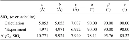
and a 666 k-mesh is used for the calculations of DOS and the dielectric response functions. After structural relaxation, the cell parameters obtained for the two systems are listed in Table 1. The geometries of the -cristobalite crystal agree well with available experimental data.25)
3. Results and Discussion
3.1 Structural characterization
We firstly examined the structural properties of the Al2O3
-SiO2 (molar ratio = 1/3). The calculated radial distribution
functions (RDF) for Si-O and Al-O are displayed in Fig. 2. The range of Si-O bond length is 1:53 ArSiO1:88 A, and the range of Al-O bond length is1:63 ArSiO1:88 A. Similar results are obtained in previous studies on Al2O3
incorporation in SiO2 network,14)where the PAW potential
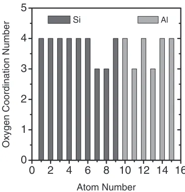
and PW91 exchange-correlation functional are employed, the same as the ones used in our calculations. The RDF peaks in Fig. 2 are not smooth curves because of the relatively small number of atoms in the unit cell. Based on the RDF data, the oxygen coordination numbers of Si and Al atoms are calculated and shown in Fig. 3. For convenience, we tag
each atom with an integer, ‘‘1’’—‘‘9’’ for Si, ‘‘10’’—‘‘15’’ for Al, and ‘‘16’’—‘‘42’’ for O atoms. The most probable oxygen coordination number for both Si and Al is four, which also agrees with previous studies.13,14) Of course, it should be noted here that, to reproduce all (or most of) the important structural properties of the real Al2O3-SiO2glasses remains a Fig. 1 (a) Atomic bonding structure of the SiO2 crystal (-cristobalite,
221unit cell). The Si atoms are represented by large (grey) balls, and the O atoms are represented by small (red) balls. Based on this structure, the Al2O3-SiO2model is constructed. The Si (marked by yellow balls) and
O atoms (marked by green balls) to be removed are labeled as ‘‘R1’’ to ‘‘R6’’, and the Si atoms (marked by blue balls) to be replaced by Al atoms are labeled by ‘‘P1’’ to ‘‘P6’’. (b) The unit cell of the Al2O3-SiO2structure
(molar ratio N(Al2O3):N(SiO2)¼1=3) obtained by DFT calculations.
[image:2.595.308.548.76.382.2]The Si atoms are represented by the largest (grey) balls, and the O atoms are represented by the smallest (red) balls, the doped Al atoms are represented by the second largest (pink) balls (marked by ‘‘Al’’). In the up and down panels, the cell axesaa~,bb~and~ccare denoted by OA, OB and OC, respectively. The seemingly isolated atoms or the atoms with dangling bonds are actually bonded with the atoms in the neighboring unit cells by periodic boundary conditions.
Table 1 The unit cell parameters of SiO2 crystal, and the Al2O3-SiO2
structure (N(Al2O3):N(SiO2)¼1 : 3). Herea,b,cdenote the lengths of
lattice vectors of the unit cell, and,,are the angles formed between the vectors.
a
(A˚ )
b
(A˚ )
c
(A˚ ) ()
()
()
SiO2(-cristobalite)
Calculation 5.053 5.053 7.037 90.00 90.00 90.00
Experiment 4.971 4.971 6.922 90.00 90.00 90.00
Al2O3-SiO2 10.771 9.924 7.949 78.11 95.76 85.22
[image:2.595.304.548.610.686.2]challenging job for DFT-level calculations, because several thousands or even larger number of atoms should be considered in the simulation unit cell. On the other hand, a recent study based on ab initio and classical molecular dynamics (MD) simulations has found that the statistical average structural features of the small glass samples of silica capture the characteristics of the large glass systems quite well.26)The aim of this work is quite modest: to find out what changes would be brought to the electronic and optical
properties by the dopants, and to suggest possible forms of the Al2O3 doped SiO2 structures that bear some important
features of the aluminosilicate glasses. It isnot our aim to simulate the real Al2O3-SiO2glasses that lack of long-range
order and are much too complex. Based on the above model, we then studied the electronic structures and optical proper-ties of the Al2O3-SiO2, which will have important
implica-tions to the doping effects of Al2O3on the SiO2crystals and
glasses.
3.2 Electronic and optical properties
Previous studies on liquid and amorphous SiO2,27,28)and
crystalline Al2O329)have demonstrated that DFT with local
density approximation (LDA) or generalized gradient ap-proximation (GGA) can provide good description for the electronic structures of the ground state. In the following paragraphs we will study the electronic and optical properties of the Al2O3-SiO2 within the framework of DFT-GGA
calculations. We stress here that, the Al2O3-SiO2 system
under consideration is saturated in the total number of electrons. This is different from the Al-SiO2system, in which
the total number of electrons is not saturated, holes induced by the Al impurities are expected and cause challenge for DFT treatment.30)
The calculated total density of states (DOS) around the valence and conduction bands of the -cristobalite crystal and the Al2O3-SiO2 are shown in Fig. 4(a) and 4(b),
respectively. We are interested in the DOS peaks around the top of valence band, i.e., the Fermi level (EF) atT ¼0K, (EF sits in-between the valence and conduction band when T >0K), which play a key role in determining the physical properties of materials under external excitation such as light
0
1
2
3
4
5
0
10
20
30
40
50
60
0
1
2
3
4
5
0
10
20
30
40
50
(a)
R
SiOg
SiO(b)
g
AlOR
AlOFig. 2 Calculated radial distribution functions (RDF) gSiOand gAlOfor the
Al2O3-SiO2structure. The unit for the separations RSiOand RAlOis A˚ .
Oxygen Coordination Number
Atom Number Si
0
2
4
6
8 10 12 14 16
0
1
2
3
4
5
Al
Fig. 3 Calculated oxygen coordination number of Si and Al atoms in the Al2O3-SiO2structure. The Si atoms are tagged by integers from ‘‘1’’ to
‘‘9’’, and the Al atoms are tagged by integers from ‘‘10’’—‘‘15’’. These integers are referred as ‘‘Atom Number’’ on the horizontal axis.
-3 0 3 6
0.0 2.5 5.0 7.5
-1.0 -0.5 0.0 0.0
2.5 5.0
-3 0 3 6
0 10 20 30
-1.00 -0.5 0.0 10
20 30
SiO2 (a)
DOS (states/eV/SiO
2
)
Al2O3-SiO2 (b)
Energy (eV)
Fig. 4 Total electronic density of states (DOS) of the SiO2 crystal (
-cristobalite, up panels) and the Al2O3-SiO2structure (down panels), which
are normalized by the number of SiO2unit. The insets display the DOS
[image:3.595.75.267.70.360.2] [image:3.595.348.509.74.328.2] [image:3.595.76.259.415.605.2]and heat. As shown in Fig. 4(a), the total DOS of pure SiO2
crystal are continuous and decrease to 0 when the energies of valence electrons approach the top of valence band. After doping with Al2O3, the DOS of Al2O3-SiO2 shows split and
discontinuous and sharp peaks around the top of valence band (Fig. 4(b)), which are highlighted by two insets in the up and down panels, with the energy scale ranging from1to 0 eV (relative to the highest occupied energy level). Similar sharp DOS peaks are also observed for the Al2O3 doped SiO2
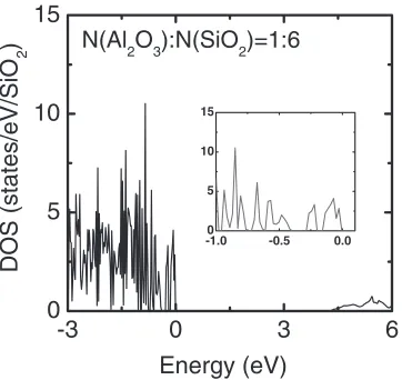
structure with a molar ratio of 1/6 between Al2O3and SiO2,
as shown in Fig. 5.
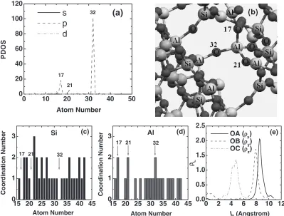
To figure out the contributions of each type of atom and the contributions from atomic orbitals to the total DOS, we plot the partial density of states (PDOS) of the s, p, d orbitals from Si, Al and O atoms of the Al2O3-SiO2in Fig. 6, from the up
panels to the down panels, with an energy range of 1 to 0 eV. By comparing the three panels, one sees clearly that the sharp peaks near the top of valence band are mainly contributed from the 2p orbitals of O atoms. Then, what kind of atomic arrangement will lead to the emergent of such split and sharp DOS peaks?
Shown in Fig. 7(a), are the PDOS contributions of each atom to the s, p, d components of the total DOS peak that is closest to the top of valence band. As before, each atom is tagged by an integer, ‘‘1’’—‘‘9’’ for Si, ‘‘10’’—‘‘15’’ for Al, and ‘‘16’’—‘‘42’’ for O atoms. The sharp DOS peak is found to be mainly contributed by the O atom tagged by the integer ‘‘32’’ (referred as O32), and two other O atoms tagged by
‘‘17’’ (referred as O17) and ‘‘21’’ (referred as O21). The
positions and bonding environment of the three O atoms are schematically shown in Fig. 7(b). The common feature is that the three O atoms are only coordinated by two Al atoms, forming the –[Al-O-Al]– linkages. The Si and Al coordina-tion numbers of each O atom in the Al2O3-SiO2structure are
displayed in Fig. 7(c) and (d), which are obtained by counting the number of Si/Al atoms around each O atom inside the first coordination shell. Both the radii of the first O-Si and O-Al coordination shell are determined to be
1:90A˚ in the calculated radial distribution functions for
O-Si and O-Al. From Fig. 7(c) and (d), one sees that the three O atoms O17, O21 and O32 are not coordinated by any Si
atoms, they are the only three O atoms that are coordinated by two Al atoms nearby, which are the largest Al coordination number in the Al2O3-SiO2. The 2p orbitals of O atoms
in such a structure as –[Al-O-Al]– are unsaturated when comparing to the O atoms in crystalline Al2O3, which is
coordinated by four Al atoms.29)On the contrary, the other O atoms with little contributions to the sharp DOS peaks near the top of valence band are either coordinated with Al and Si atoms, or with Si atoms only, corresponding to the saturated or nearly saturated bonding of the O 2p orbitals. We have calculated the number of electrons within a sphere centered at O atom with a radius of 1.2 A˚ , the counted electrons of O in the –[Al-O-Al]– linkage is about 0.3 electron less than in the –[Si-O-Si]– structure, which again demonstrating at least one 2p orbital in the –[Al-O-Al]– linkage is unsaturated. In Fig. 7(a), the O atom O32contributes to the major part of the
PDOS comparing to the other two O atoms O17and O21. This
may originate from the fact that the O atom O32 is the most
loosely bonded with Al among the three O atoms coordinated by two Al. The minimum O-Al bond length of O32is 1.71 A˚ ,
and the minimum O-Al bond length for the O atoms O17and O21is 1.66 A˚ and 1.63 A˚, respectively. Another factor is that the O32is sitting in-between two cavity structures (Fig. 7(b)), which makes the –[Al-O-Al]– linkage formed by the O32has a much larger contact space with vacuum comparing to the other two –[Al-O-Al]– linkages. Such a vacuum/atom
-3
0
3
6
0
5
10
15
-1.00 -0.5 0.0
5 10 15
DOS (states/eV/SiO
2
)
Energy (eV)
N(Al2O3):N(SiO2)=1:6
Fig. 5 Total DOS of the Al2O3-SiO2structure, whose unit cell consists of
46 atoms: 12 Si atoms, 4 Al atoms, and 30 O atoms, with a molar ratio of 1/6 between Al2O3and SiO2. The inset shows the DOS from1to 0 eV.
The energy 0 eV is set to the top of valence band.
0 1 2 3
0 2 4 6 8
-1.00 -0.5 0.0 2 3 4 5 30
60 90 120 150
0 1 2 3
0 1 2 3
2.0 2.5 3.0 3.5 4.0
0 1 2 3
s Si
p d
Al s p d
O
PDOS (states/eV/unitcell)
s p
Energy (eV)
d s p
d
Fig. 6 Partial density of states (PDOS) contributed from the Si, Al and O atoms in the Al2O3-SiO2structure. The energy 0 eV is set to the top of
[image:4.595.80.261.74.245.2] [image:4.595.340.512.76.379.2]structure provides a potential well for electron trapping. The PDOS contribution peaks in Fig. 7(a) also indicate that the wave function of the electron states should exhibit localized features. To demonstrate this point, we have further analyzed the band decomposed charge density (partial electron density) of the DOS peaks near the top of valence band. Figure 7(e) shows the calculated linear charge density of the highest occupied electronic energy band, along the three lattice vectors directions OA (aa~), OB (bb~) and OC (cc~) of the unit cell. Obviously, the linear electron density (and thus the wave function) vanishes quickly as the distances to the density peaks are increased. From the peak positions along the OA, OB and OC direction, the center of the wave package that has the highest electron density is determined as (8.527 A˚ , 7.902 A˚, 4.769 A˚). This is close to the position of the O labeled as ‘‘32’’ in Fig. 7(b), whose Cartesian coordinates in the unit cell are (8.542 A˚ , 8.687 A˚, 4.677 A˚). The displacement of the center of electron wave package and the nuclear position of the O32will induce an electric dipole
moment, which is estimated to be PP~ ð2eÞðrre~ rr~OÞ ¼
ð0:14;7:54;0:88ÞDebye. Such an electron energy state with localized characteristics sits near the O32 atom in Fig. 7(b). In addition, the possibility of spin polarization is ruled out because our calculations show that no energy difference is found between non-spin-polarized states and spin-polarized states. Similar results are obtained for other isolated and
sharp DOS peaks near the top of valence band, and we expect the results can be demonstrated by future experiments such as electron paramagnetic resonance (EPR).
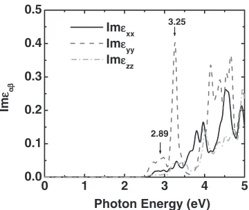
We go further to study the optical properties of the Al2O3
-SiO2 structure, by calculating the frequency-dependent
dielectric functions within the DFT framework. The imag-inary part of the dielectric function (33 tensor) describes the optical absorption in condensed phase materials,31)whose
xx, yy and zz components in the Al2O3-SiO2 are plotted
as a function of photon energies in Fig. 8. In the visible range, two peaks are observed at 2:89 and 3.25 eV. This corresponds to the optical transition of electrons from the highest valence band to the bands identified by the two isolated DOS peaks, which emerge at2:8and 3.2 eV above the top of valence band (Fig. 4(b) & Fig. 6). Our PDOS analysis reveals that the two isolated DOS peaks in-between the valence bands and conduction bands in Fig. 4(b) come mainly from the hybridization of the 2s orbitals of O and 3s orbitals of Si, the 2p orbitals of O and 3d orbitals of Si. Using the selection rule for optical transition, the absorption in visible range should mainly come from the quantum transition of the p orbitals of O atoms (valence band) to the s orbitals of O and Si, and the d orbitals of Si atoms, as can be inferred in Fig. 6. The optical absorption in visible range alongydirection is much stronger than inxandzdirections (Fig. 8). The much stronger electric dipole moment PP~iny
0 10 20 30 40 50
0 20 40 60 80 100 120
(a)
32
21 17
PDOS
Atom Number
s
p
d
15 20 25 30 35 40 45 0
1 2 3
0 2 4 6 8 10 12
0.0 0.5 1.0 1.5 2.0 2.5
Coordination Number
(c)
32 21
17
Coordination Number
Atom Number
Si
15 20 25 30 35 40 45 0
1 2
3 (d)
32 21
17
Atom Number
Al OA(ρx)
ρ L
L (Angstrom)
OB(ρy)
(e)
OC(ρz)
Fig. 7 (a) PDOS contributions of each atom to the highest occupied valence band in the Al2O3-SiO2structure. (b) Bonding structures of
the –[Al-O-Al]- linkages in the Al2O3-SiO2. The surrounding Si atoms (largest, gray balls), Al (second largest, pink balls), O (smallest,
red balls) are also marked. This schematic diagram is obtained by extending the unit cell in Fig. 1(b) and then cut out the part with –[Al-O-Al]- linkages. (c)&(d) The Si and Al coordination number of each O atom in the Al2O3-SiO2. (e) The linear electron density (L)
[image:5.595.98.497.75.378.2]direction thanxandzdirections induced by the electron state near the top of valence band should be responsible for this anisotropy of light absorption, due to the fact that optical absorption in visible range is mainly caused by electric dipole transition. It should be noted here that an accurate quanti-tative description of the optical properties requires a treat-ment such as GW,32) which is beyond the independent particle approximation. On the other hand, the qualitative agreement between theory and experimental results can usually be achieved on the DFT level calculations, i.e., DFT-LDA/GGA calculations can usually give correct description for the energy dispersion relation in the k-space, and the band energies obtained by GW calculations are usually shifted up by a constant comparing to the DFT-LDA/GGA energy bands.32–34)
4. Conclusions
To summarize, we have studied the structural, electronic and optical properties of the Al2O3 doped SiO2 by DFT
calculations. The Al2O3-SiO2 model used in our studies has
captured the important features for Si-O and Al-O bonding in the real Al2O3-SiO2 glasses. By doping with Al2O3, the
electronic structures of the SiO2 crystal are reformed
significantly: sharp DOS peaks emerge near the top of valence band. Partial density of states (PDOS) analysis shows that the sharp DOS peaks are mainly contributed by the unsaturated 2p orbitals of the O atoms in the –[Al-O-Al]– linkages. The electronic energy states near the top of valence band are found to exhibit localized characteristics. The optical absorption of the Al2O3-SiO2 structure has been
studied by calculating the imaginary part of the frequency-dependent dielectric function, whose features are found to be correlated with the new DOS peaks in-between the valence and conduction bands, and the electric dipole moments induced by the electron states near the top of valence band. Our studies shed new light to the doping effects of Al2O3on
SiO2, i.e., the electronic density of states near the top of
valence band can be significantly modified with the presence of the –[Al-O-Al]– linkages. This makes it possible to manipulate the response properties of the materials under
external excitations such as electron heat capacities and optical absorption.
Acknowledgment
We are grateful to the staff of the Center for Computational Materials Science at Institute for Materials Research of Tohoku University. One of us (Y. Y.) is supported by the Center for Special Field Research, Tohoku University. We thank Dr. J. Furthmu¨ller for providing the program optics.F to calculate the dielectric function, and Mr. R. Note, Dr. M. S. Bahramy and Dr. Sheng Meng for their helpful discussions while compiling the program optics.F. We also thank Professor Vijay Kumar for his valuable comments.
REFERENCES
1) E. K. Chang, M. Rohlfing and S. G. Louie: Phys. Rev. Lett.85(2000) 2613.
2) M. G. Ferreira da Silva: J. Non-Cryst. Solids352(2006) 807. 3) S. Berneschi, M. Bettinelli, M. Brenci, G. N. Conti, S. Pelli, S.
Sebastiani, C. Siligardi, A. Speghini and G. C. Righini: J. Non-Cryst. Solids351(2005) 1747.
4) S. Sen and J. F. Stebbins: J. Non-Cryst. Solids188(1995) 54. 5) R. H. D. Nuttall and J. A. Weil: Can. J. Phys.59(1981) 1696. 6) R. S. Dickson and J. A. Weil: Can. J. Phys.68(1990) 630.
7) D. F. Howarth, M. J. Mombourquette and J. A. Weil: Can. J. Phys.75
(1997) 99.
8) S. Sen: J. Non-Cryst. Solids261(2000) 226.
9) M. Schmu¨cker, H. Schneider and K. J. D. MacKenzie: J. Non-Cryst. Solids226(1998) 99.
10) K. L. Brower: Phys. Rev. Lett.41(1978) 879.
11) T. Schaller and J. F. Stebbins: J. Phys. Chem. B102(1998) 10690. 12) J. Jin, S. Sakida, T. Yoko and M. Nogami: J. Non-Cryst. Solids262
(2000) 183.
13) M. Benoit, S. Ispas and M. E. Tuckerman: Phys. Rev. B64(2001) 224205.
14) J. Lægsgaard: Phys. Rev. B65(2002) 174104. 15) V. V. Hoang: Phys. Rev. B75(2007) 174202. 16) G. Kresse and J. Hafner: Phys. Rev. B47(1993) 558. 17) G. Kresse and J. Hafner: Phys. Rev. B49(1994) 14251. 18) G. Kresse and J. Furthmu¨ller: Comput. Mater. Sci.6(1996) 15. 19) G. Kresse and J. Furthmu¨ller: Phys. Rev. B54(1996) 11169. 20) P. E. Blo¨chl: Phys. Rev. B50(1994) 17953.
21) G. Kresse and D. Joubert: Phys. Rev. B59(1999) 1758.
22) J. P. Perdew, J. A. Chevary, S. H. Vosko, K. A. Jackson, M. R. Pederson, D. J. Singh and C. Fiolhais: Phys. Rev. B46(1992) 6671. 23) S. Berneschi, M. Bettinelli, M. Brenci, G. N. Conti, S. Pelli, S.
Sebastiani, C. Siligardi, A. Speghini and G. C. Righini: J. Non-Cryst. Solids351(2005) 1747.
24) H. J. Monkhorst and J. D. Pack: Phys. Rev. B13(1976) 5188. 25) R. T. Downs and D. C. Palmer: Am. Mineral.79(1994) 9.
26) R. M. Van Ginhoven, H. Jo´nsson and L. R. Corrales: Phys. Rev. B71
(2005) 024208.
27) J. Sarnthein, A. Pasquarello and R. Car: Phys. Rev. Lett.74(1995) 4682.
28) J. Sarnthein, A. Pasquarello and R. Car: Phys. Rev. B52(1995) 12690. 29) B. Holm, R. Ahuja, Y. Yourdshahyan, B. Johansson and B. I.
Lundqvist: Phys. Rev. B59(1999) 12777.
30) J. Lægsgaard and K. Stokbro: Phys. Rev. Lett.86(2001) 2834. 31) M. Gajdosˇ, K. Hummer, G. Kresse, J. Furthmu¨ller and F. Bechstedt:
Phys. Rev. B73(2006) 045112.
32) M. S. Hybertsen and S. G. Louie: Phys. Rev. B34(1986) 5390. 33) R. M. Martin:Electronic Structure(Cambridge University Press, 2004)
pp. 43.
34) A. J. Lu and R. Q. Zhang: Solid State Commun.145(2008) 275.
0 1 2 3 4 5
0.0 0.1 0.2 0.3 0.4 0.5
Im
εαβαβ
Photon Energy (eV) Imεxx
Imεyy
2.89 3.25
Imεzz
[image:6.595.80.260.72.224.2]