SYS68K/ ASCU-l/2
HARDWARE USER'S MANUAL
NOT E
The information in this document has been carefully checked and is believed to be entirely reliable. FORCE COMPUTERS makes no
warranty of any kind with regard to the material in this
document, and assumes no responsibility for any errors that may appear in this document. FORCE COMPUTERS reserves the right to make changes without notice to this, or any of its products, to improve reliability, performance or design.
FORCE COMPUTERS assumes no responsibility for the use of any circuitry other than circuitry which is part of a product of FORCE COMPUTERS GmbH/Inc.
FORCE COMPUTERS does not convey to the purchaser of the product described herein any license under the patent rights of FORCE COMPUTERS GmbH/Inc. nor the rights of others.
FORCE COMPUTERS Inc. 727 University Avenue Los Gatos, CA 95030 U.S.A.
Phone Telex FAX
(408) 354 34 10 172465
(408) 395 77 18
FORCE COMPUTERS GmbH Daimlerstrasse 9
D-8012 Ottobrunn/Munich West Germany
Phone Telex FAX
(089) 6 09 20 33 5 24 190 forc-d
(0 89)6 09 77 93
FORCE COMPUTERS FRANCE Sarl 11, rue Casteja
92100 Boulogne France
Phone Telex Fax
(1) 620 37 37 206 304 forc-f
1. 1.1 1.2 2. 2.1 2.2 2.3 3. 3.1 3.2 3.3 3.4 3.5 3.6 3.7 3.8 4. 4.1 4.2 4.3 5. 5.1 5.2 5.3 6. 7. 7.1 8. 8.1 9. 10. 10.1 10.2 10.3 11.
Index of Contents
General Description SYS68K/ASCU-l/2 •••••••••••• Features of the SYS68K/ASCU-l ••••••••••••
Features of the SYS68K/ASCU-2 ••• Additional
Access to the SYS68K/ASCU-l/2 •• Board Base Address Selection ••• Address Modifier Decoding.
Application Example •••••••
The Front Panel ••••• RESET Function Switch •• TEST Function Switch .• The SYSFAIL LED •••••••• The ACFAIL LED ..••••••• Bus Arbitration Status LEOs. The T/L Switch •.•.•••••••••• IEEE 488 GPIB Connector .•••• Serial Interface Connector •••
Interrupt Structure of the SYS68K/ASCU-l/2 .••••.••. Programming of the BIM on the ASCU-l/2 .•••••••••••• Interrupt Sources and lACK Daisy Chain Structure of the SYS68K/ASCU-l/2 •••••••••
Interrupt vector Structure... • ••••
Utility Signal Handling •• The SYSRESET* Signal •••••••• The SYSFAIL* Signal .•
The ACFAIL* Signal ••••
Functional Groups on the SYS68K/ASCU-l/2.
Software Control •••••••••••.•.• Addressing of the PI/T Devices ••
Power Monitor Module •• The RESET Generator ••
The SYSCLOCK Driver ••
The 4-Level Bus Arbiter •••
The PRI Arbiter ••
. . .
..
. .
The RRS Arbiter ••
. . . .
. . .
.
The PRR Arbiter ••
. . .
.
.
. . .
.
. . . .
.
. .
. .
...
The Bus Timer •••
. . .
. . .
. .
.
. . . .
.
. . .
13. 13.1 14. 14.1 14.2 14.3 15. 15.1 15.2 15.3 16. 17. 17.1 17.2 17.3 17.4 17.5 18. 19. 19.1 19.2 20. 21. 22.
Index of Contents cont'd
Centronics Interface ••••••••••••••••••••••••••• Interrupt Scheme of the Centronics Interface •• The Real Time Clock ••
Features of the RTC ••• Timing of the RTC ••••• The RTC Interrupt Scheme •• Special Interrupts •••••• The TEST Interrupt •••••• The User Interrupt 1 ••••
The User Interrupts 2-5.
· . . .
. .
...
. . .
· . . .
.
. . .
Timer Interrupt •••••••••
· . .
. . .
. .
. . .
. .
. .
.
.
.
.
The IEEE 488 GPIB Interface ••••••••••••••••••Features of the NEC 7210 ••••••••••••••••••••• Hardware Realization of the GPIB Interface ••• Addressing of the GPIB Controller •••••••••••• The GPIB Interrupt Scheme •••••••••••••••••••• Programming Example of the GPIB Controller ••• Software Programmable Interrupts.
The BCLR* Timing Function •••••••• BCLR* Signal Generation Structure •••• The BCLR * Timer •••••••••••••••••••••• Board Register Summary.
General Information •••••••••••••••••
Installation of the SYS68K/ASCU-l/2.
.
.
.
.
. . .
APPENDIX:
A: Specification of the SYS68K/ASCU-l/2
B: Address Assignment of the SYS68K/ASCU-l/2 Devices
C: Description of the Jumperfields
D: PIN-Assignment on the SYS68K/ASCU-l/2
E: Circuit Schematics
F: Component Part List SYS68K/ASCU-l/2
G: Glossary of VMEbus/P1014 Terms
H: Data Sheets
I: Product Error Report
68153 68230 68561 58167A 7210
List of Figures
Fig.# Page
1 Photo of the SYS68K/ASCU-l/2 Board ••••....•....••••.•• 12
2 Block Diagram of the SYS68K/ASCU-l .••....•....•..•..•• 15
3 Block Diagram of the SYS68K/ASCU-2 . . . • • . . . • . . • • . . . • . 17
4 Jumper Location Diagram for the Board Base Address Selection. . . . . 20
5 Board Base Address Selection .•..•.•.••...••..•..•... 21
6 Jumper Location Diagram for the Address Modifier Code S e l e c t i o n . . . 27
7 Address Modifier Code Selection .••..••.•.••••..•.•..•• 28
8 The Front Panel of the SYS68K/ASCU-2 .••.•....•....•••. 32
9 Jumperfield Location Diagram of B4 and B19 ...•••...• 40
10 The SYSRESET Jumperfield B16 and the Jumperfield B9 for the first External RESET Switch Connection ....••.. 50
11 Jumperfield B30 for Selection of the Centronics Interface / second Optional RESET Switch •.•.•.•....•.. 52
12 Jumper Locations of the ACFAIL* Signal Handling B10, B12, B13 and B l S . . . 59
13 System Block Diagram... 71
14 Power Fail Timing Diagram... 72
15 Block Diagram of the RESET Structure .•...•••.••••.. 74
16 Power Monitor System Restart Timing ••.•.•...••••..• 75
List of Figures cont'd
Fig.# Page
24 Location Diagram of the Serial I/O Interface Parts •... 98 25 Signal Assignment of Jumperfield B37 ••••••••.•.•.••••• 100
26 Serial I/O Hardware Lay-out .•.••••.•.•.•.••••••••••.•. 101
27 The Optional R/C Implementation •.•••.•..•.•.••.•..•.•. 102
28 Connection between the SYS68K/ASCU-l/2 Board and a
Termina 1 . . . .. 104
29 Timing Diagram of the Centronics Parallel Interface ... 110 30 Hardware Realization of the Centronics Interface •.•.•. 111 31 Connection Example for the Centronics Interface ••••••• 113 32 Location Diagram of the Centronics Interface
Components. . . . .. 114
33 Location Diagram of the Jumperfield B31 and the
Battery position ••.•••••••••••••..••••••••••••••••••.• 118 34 RTC Write Cycle Timing Diagram ..•••••••.••••••••.•.••• 122 35 RTC Read Cycle Timing Diagram .••..•..••.•..••.•.•.•... 124
Table #= List of Tables Page
1 Board Base Address Selection . . . . 22
2 Address Modifier Codes .••••••.••.••••••••.•••.•••••.•• 24
3 Address Modifier Code Selection ..••••••••••••••••••••. 26
4 IEEE 488 Connector Pin Assignment ••••••••.••.••••••.•. 35 5 Default I/O Signal Assignment to the D-Sub-Connector.. 36 6 Sequence of the On-Board lACK Daisy Chain •.•.••••.•.•• 43
7 Non-Vectorized Interrupt Sources ••••.•••.•••.•••..•••• 45
8 Vectorized Interrupt Source •••••••••••••••••••..•... 46
9 Optional Vectorized Int~~rupt Source 1 •.•••••.•••••••• 47 10 optional Vectorized Interrupt Source 2 ..•••••....•.... 47
11 RESET* on the ASCU-l/2... 48
12 The Power Fail Signal Level •••••.••••••••••.••.••••.•. 56 13 ACFAIL* Interrupt Channel Address Assignment •••••••••• 57 14 Delay of the SYSRESET* Generation after ACFAIL* ••••••. 58
15 Functional Group Distribution •...•••••••••••••••.••••• 63
16 Software Control I/O pins .•••.•••••••••.•••••••••••••• 67 17 Selection of the Arbitration Type ..••••••••••••••••••• 79 18 Jumper Selection for Enabled Bus Arbiter Function .•••• 80 19 Jumper Selection for Disabled Bus Arbiter Function .••• 81 20 BCLR* Generation on the SYS68K/ASCU-l .••••••••••••••.• 83
Table #: Page 28 Power Connection for the RTC •••••••••••••••••••••••••• 117
29 Register Table of the RTC ••••••••••••••••••••••••••••• 120
30 RTC Write Time Values ••••••••••••••••••••••••••••••••• 121
31 RTC Read Time V a l u e s . . . 123 32 RTC Interrupt Channel Address Assignment •••••••••••••• 125 33 TEST Interrupt Channel Address Assignment ••••••••••••• 126
34 TIMER Interrupt Channel Address Assignment •••••••••••• 131 35 GPIB Interface Capabilities •••••••••••••••••••• ' ••••.•• 135
36 GPIB Address Selection •••••••••••••••••••••••••••••.•• 138
37 IEEE 488 Connector PIN Assignment .•••••••••••••••••••• 140 38 Register Table of the GPIB Controller ••••••••••••••••• 141 39 GPIB Controller Interrupt Channel Address Assignment .• 142
40 GPIB Interrupt Events •••.••••••••••••••••••••••••••••• 143
41 42 43 44 45
46
The Software Programmable Interrupts of the ASCU-2 •••• BCLR* Generation Modes in the PRI Arbitration Type •••• BCLR* Generation Modes in the RRS Arbitration Type •••• BCLR* Generation Modes in the PRR Arbitration Type •••• The MPCC Address Map in the Byte Mode of Addressing .••
The MPCC Address Map in the Word Mode of Addressing ••• 146 150 151 152
ISS"
156 47 The PI
IT
1 Address M a p . . . 158 48 The PIIT
2 Address M a p . . . 160 49 The RTC Address M a p . . . 16250 The GPIB-Controller Address Map •••••••••.••••••••••.•• 164
51 52 53
The The The
BIM BIM BH1
1
2 3
Register Register Register
Table . . . Table . . . Tabl e . . .
1. General Description SYS68K/ASCU-l/2
The SYS68K/ASCU-l board is a high performance system controller which handles all exception signals on the VMEbus and contains powerful I/O devices such as a serial interface (RS232 and RS422 compatible), a centronics parallel interface, a real time clock with battery backup, and a 4 level bus arbiter.
The SYS68K/ASCU-2 board provides all the features of the ASCU-l board as well as a IEEE 488 GPIB interface with Talker, Listener, and Controller functions and powerful interrupt capabilities for multiprocessor environments.
1.1 Features of the SYS68K/ASCU-l
- 4 level Bus ARBITER with prioritized,
prioritized round robin operating mode.
round robin, and
- LEDs show the current bus master level (0-3)
- High speed serial I/O channel
Communications Controller, RS232
circuitries.
with
and RS422 68561
Multi-Protocol driver/receiver
- Centronics Parallel Interface for printer connection
- 58167A Real Time Clock with on-board battery back-up
- POWER MONITOR provides automatic power-up/power-down and
ACFAIL/SYSRESET handling through power fail detection. A Reset function switch generates a SYSRESET to the VMEbus.
- SYSTEM CLOCK driver (16MHz)
- BUS TIMER with software selectable time-outs for Bus Error generation
- Timer Interrupt can be used for time measurements or as a watch dog
- Software selectable option for generating an interrupt on
ACFAIL detection
Figure 2: Block Diagram of the SYS68K/ASCU-l
INTER·
RUPT
CON·
1.2 Additional Features of the SYS68K/ASCU-2
- All of the features contained in the SYS68K/ASCU-l description
- General Purpose Interface Bus (IEEE488) Talker, Listener, and Controller functions
- 8 different fully software programmable interrupts to the
VMEbus
- 5 user interrupts (buffered inputs through P2 connector)
- Software programmable time-out for bus mastership of the
2. Access to the SYS68K/ASCU-l/2
The SYS68K/ASCU-l/2 is accessible under a user defined address and Address Modifier Code.
The decoding includes the Standard Decoding Mode, with an address range of 16Mbytesand short I/O range with 64 Kbytes address range.
To access the board, the jumper settings for the Board Base
Address and the Address Modifier Code must match the valid
address and Address Modifier Code on the VMEbus. The board is
delivered with a default Board Base Address of $B02000. The default jumper setting for the Address Modifier Code is the mode in which the SYS68K/ASCU-l/2 responds to any defined Address Modifier Code.
The SYS68K/ASCU-I/2 occupies an Address Range of 512 bytes,
beginning at the Board Base Address. However, within this
2.1 Board Base Address Selection
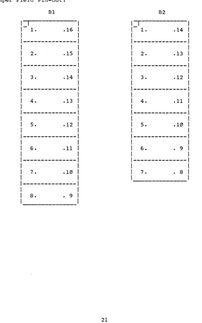
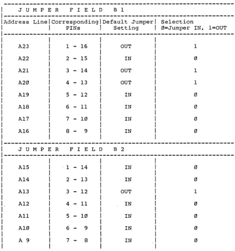
The Base Address of the SYS68K/ASCU-l/2 is jumper selectable in the l6Mbyte address space, in steps of 512 bytes. To select the board, the address on the address lines A9-A23 must match the base address jumper settings at jumper fields Bl and B2.
Bl is the jumper field which defines the bit pattern of the address lines A23-A16. B2 is the jumper field for the address lines A15-A9.
Fig. 4 shows the location of the jumper fields Bl and B2 on the PC board.
Fig. 5 shows the pinout of the jumper fields Bl and B2.
Table 1 points out the connection assignment:
"IN" stands for a connection of the associated pins by a
plugged-in jumper,
Figure 4: Jumper Location Diagram for the Board Base Address Selection
:r
c..
J7b
I
Ll-h _J7_B - - - - IPut
h
J3CI
'-' J75 U Jb
LJ1
6 1 0
C"') C"')
a>
"'
...
B3~Ih
6
I
7 (;lb
M
J29
o
h
J5 '-'C"') ~
I
...,
n
J'i9om
~h
ij~ I-
I
U J5D
a>
..,
-q[
~-J3-D----O--CI3----~~~~lJ_ID-J9--~·
C'i9~ .
-:8
en '-'
-LJ1
a>-~o~nc
'-'
c6r
uma:
Figure 5: Board Base Address Selection
Jumper Field Pin-out:
I
1.
2.
3.
4.
5.
6.
7.
8.
Bl
.16
. 15
• 14
.13
.12
.11
• 10
• 9
B2
I
1 • .14
2 • .13
3. .12
4. .11
5. .10
6. • 9
[image:21.620.110.516.110.758.2]Table 1: Board Base Address Selection
Default Base Address : $B02000
1 JUMPER FIELD Bl 1
1---1
IAddress LinelcorrespondinglDefault Jumper 1 Selection 1
1 PINs 1 Setting 1 0=Jumper IN, l=OUT 1
---1
A23 1 - 16 OUT 1
A22 2 - 15 IN
A21 3 - 14 OUT 1
A20 4 - 13 OUT 1
A19 5 - 12 IN
Ala 6 - 11 IN
1
A17 7 - 10 IN 0 1
1
A16
a -
9 IN 0I
I
---1
J U M PER F I E L D B 2
A15 ·1
-
14 IN 0A14 2
-
13 IN 0I
1 A13 3
-
12 OUT 11
I.
A12 4-
11 IN 01
[image:22.617.65.523.134.624.2]2.2 Address Modifier Decoding
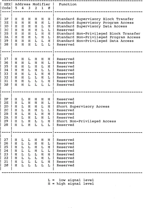
The VMEbus has 6 signal lines (AM0-AMS) carrying the Address Modifier Code which is generated by the bus master together with the address signals. The definition of the AM codes is given in table 2.
The SYS6SK/ASCU-I/2 can be accessed with several AM codes,
according to the jumper settings in the field B7 and BS. The following AM codes are decoded and selectable as described in
table 3. At least one jumper must be inserted, and any
combination is allowed. Therefore, .the board is able to respond to several AM codes without changing the jumper settings.
Figure 6 outlines the jumper location diagram of the AM jumper field B7 and BS.
Figure 7 shows the pin numbering of B7 and BS.
The default setting in the AM jumper field during manufacturing is as shown in table 3, which causes the board to ignore the AM code.
Table 2: Address Modifier Codes
---HEX Code 3F 3E 3D 3C 3B 3A 39 38 37 36 35 34 33 32 31 30 2F 2E 2D 2C 2B 2A 29 28 27 26 25 24
Address Modifier Function
5 4 3 2 1 0
---
---H H H H H H Standard Supervisory Block Transfer H H H H H L Standard Supervisory Program Access H H H H L H Standard Supervisory Data Access
H H H H L L Reserved
H H H L H H Standard Non-Privileged Block Transfer
H H H L H L Standard Non-Privileged Program Access H H H L L H Standard Non-privileged Data Access
Ii H H L L L Reserved
---
---H H L H H H Reserved
H H L H H L Reserved
H H L H L H Reserved
H H L H L L Reserved
H H L L H H Reserved
H H L L H L Reserved
H H L L L H Reserved
H H L L L L Reserved
---
---H L H H H H Reserved
Ii L .H H H L Reserved
H L H H L H Short Supervisory Access
H L H H L L Reserved
H L H L H H Reserved
H L H L H L Reserved
H L H L L H Short Non-Privileged Access
H L H L L L Reserved
---
---H L L H H H Reserved
H L L H H L Reserved
H L L H L H Reserved
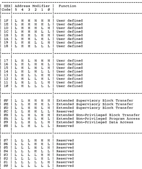
[image:24.617.64.527.72.744.2]Table 2 cont'd
---1 HEX Address Modifier Function
1 Code 5 4 3 2 1 0
1---- ---
---1
1 IF L H H H Ii Ii User defined
1 IE L Ii H Ii Ii L User defined
1 1D L Ii H Ii L H User defined
lC L H H H L L User defined
lB L H Ii L H Ii User defined lA L Ii Ii L H L User defined
19 L H H L L H User defined
18 L H Ii L L L User defined
--- ---1
1
17 L H L H H H 1 User defined 1
16 L H L Ii H L User defined 1
15 L H L Ii L H User defined 1
14 L H L Ii L L User defined
I
13 L H L L H H User defined
I
12 L H L L H L User defined
I
11 L H L L L Ii User defined 1
10 L H L L L L User defined 1
1
--- ---1
1
0F L L H Ii H H Extended Supervisory Block Transfer 1
0E L L H H H L Extended Supervisory Block Transfer 1
0D L L H Ii L H Extended Supervisory Block Transfer 1
0C L L H Ii L L Reserved 1
0B L L H L H H Extended Non-Privileged Block Transfer
I
0A L L H L Ii L Extended Non-Privileged Program Access 1
09 L L H L L H Extended Non-Privileged Data Access 1
08 L L H L L L Reserved 1
1
--- ---1
1
07 L L L H H H 1 Reserved 1
06 L L L H Ii L 1 Reserved 1
05 L L L H L H 1 Reserved 1
04 L L L Ii L L 1 Reserved 1
03 L L L L H H 1 Reserved
I
02 L L L L H L 1 Reserved 1
01 L L L L L H 1 Reserved 1
00 L L L L L L 1 Reserved 1
1 1
---T = low signal level
[image:25.620.97.560.85.637.2]Table 3: Address Modifier Code Selection
AM Code I Function
HEX
I
I Jumper- I PINS I Decoded I I field I I Address II
I I I Lines I---1
I
3D Standard Supervisory Data B7 1-8 Al-A23I
Access I
I
I
39 Standard Non-privileged B7 2-7 Al-A23I
Data Access I
2D Short Supervisory I/O Access B7 3-6 Al-A15
29 Short Non-privileged I/O B7 4-5 Al-A15
Access
xx
*
Ignore any code B8 1-4 Al-A233F Standard Access Mode for CPU B8 2-3 Al-A23
boards which do not drive the AM signal lines. This AM code is not decoded in the sense of the P10l4 Block Transfer Definition.
[image:26.617.66.528.90.506.2]Figure 6: Jumper Location Diagram for the Address Modifier Code Selection
•
6
J3J7b
16
'-'-
_J7B _____I
~ iRffi
fril
J7S w Jb
g
1 0 M'"' b a:h 83
{6 6
7 1.1b
°h
JS MM J29 ~
J'I9
I
....,
0
Om ~
6
~ L .J5DJ
'"'I I I RS 1
OW
' - - 1 I
J28
J31
U - - - . . . JiE r--h - - - , ;
Om ~I
t
N·r--b - - - ,Pll
...-
---~-
JlD~:'-'---r=u....6==-==-==-~::;-'~
~
JlIl C2'II
h
J9C'I9[); L.L....-_ _ ~
l
Jbben :8 =! enw
-1.1>
, " ,
-IZI
~pc
... 0
[image:27.620.76.537.47.735.2]Figure 7: Address Modifier Code Selection
Jumper Field Pin-out:
B7: 1 I
1-
1. . 81
1 1
1---1
1 1
1 2. . 7 1
1 1
1---1
1 1
1 3. • 6 1
1 1
1---1
1 1
1 4. • 5 1
1 _ _ _ _ _ _
-B8: 1 1
,- 1. . 4 1
1 1
1---1
1 1
1 2. • 3 I
2.3 Application Examples
Example I}:
If the Board Base Address has to be changed to $A57400 and the board should operate with the Standard Supervisory Data Access (AM Code: $3D) as well as the Standard Non-Privileged Data Access (M1 Code: $39), then the following jumper settings have to be provided:
Address Jumper
Line Setting Selection
Jumper Field Bl: A23 OUT 1
A22 IN 0
A21 OUT 1
A20 IN 0
A19 IN 0
A18 OUT 1
A17 IN 0
A16 OUT 1
Jumper Field B2: A15 IN 0
A14 OUT 1
A13 OUT 1
A12 OUT 1
All IN 0
A10 OUT 1
A 9 IN 0
Jumper Field B7: AM-Code (HEX) Connected PINs
3D 1-8
Example 2):
In this example, the Short Board Base Address $1600 with the AM-Code for Short Non-Privileged I/O access ($29) is selected. It is irrelevant, in this case, which jumper settings are made in the field Bl, because the address lines A16-A23 will not be decoded.
The following jumper connections have to be installed:
Address Jumper
Line Setting Selection
Jumper Field B2: A15 IN 0
A14 IN 0
A13 IN 0
A12 OUT 1
A19 IN 0
A10 OUT 1
A 9 OUT 1
Jumper Field B7: AM-Code (HEX) Connected PINs
3. The Front Panel
3.1 RESET Function Switch
The switch on the top of the SYS68K/ASCU-l/2 front panel is the
RESET function switch. Pushing this switch can generate a
SYSRESET* signal to the VMEbus, and resets all devices on the SYS68K/ASCU-l/2. The SYSRESET* signal is signaled by the red
RESET LED on the front panel (Figure 8). For further
information, please refer to chapter 8 - "Utility Signal
Handling" and "Power Monitor Module".
3.2 TEST Function Switch
The second switch on the front panel is the TEST function switch. It generates an interrupt request to the VMEbus. The interrupt level and vector is software programmable. The TEST function is
inactive after the power-up procedure. For correct operation
please refer to chapter 15 - "TEST Interrupt".
3.3 The SYSFAIL LED
The red SYSFAIL LED signals the status of the -corresponding Utility Bus Signal Line SYSFAIL*.
This signal line is used to indicate that a local self test of a board is in progress, or a system test has been started by an intelligent master board. During this test procedure the signal line is driven low.
The SYSFAIL* line may be driven by any module in the system that is able to detect faults.
It may also be driven low at any time during normal operation to indicate that some kind of failure has occurred. Further details can be found in chapter 5.
3.4 The ACFAIL LED
The red ACFAIL LED is built onto the SYS68K/ASCU-l/2 board as a visual indicator of power failures. The LED will signal a power failure when the ACFAIL* signal line is asserted.
Figure 8: The Front Panel of the SYS68K/ASCU-2
0
0
0
0
0
0
0
0
0
0
0
0
,....-
'--;A
0 0 0 0 0 0 0 0 0 0 0 0 0 0
o~
~
RESET function switch
TEST function switch
RESET Indication LED
sysFAIL Indication LED
ACFAIL Indication LED
BFREE LED
BCLR LED
LEV 3 LED
LEV 2 LED
LEV 1 LED
LEVOLED
TIL function switch
IEEE-488
GPIB Interface
Serial 110
3.5 BUS ARBITRATION STATUS LEOs
The SYS68K/ASCU-l/2 is equipped with six Bus Arbitration Status LEOs which show the activity of the Bus Arbiter and the bus load. The LEDs are designated on the front panel as follows:
The BUSFREE terminated, Further on, line.
BFREE (green)
BCLR ( red)
LEV 3 (yellow)
LEV 2 (yellow)
LEV 1 (yellow)
LEV
"
(yellow)LED turns on after the power-up
when the SYSRESET* signal line has the BUSFREE LED is controlled by the
procedure is been cleared. BBSY* signal
This signal line is driven to a high level if no Bus Master has control of the Data Transfer Bus. On this condition, the BUSFREE LED will light up.
The asserted BBSY* signal line indicates that a Bus Master has control of the Data Transfer Bus and the BUSFREE LED will turn off.
The BUSFREE LED will also turn off if the SYSRESET* signal line is asserted.
The BCLR (Bus Clear) LED signals the asserted BCLR* signal which is either generated by the on-board ARBITER or the BCLR-Timer.
(The BCLR-Timer is installed only on the SYS68K/ASCU-2).
To monitor operating, to LEV 0}.
the level on which the current Bus Master is
the SYS68K/ASCU-1/2 provides four yellow LEDs, (LEV 3
These LEDs are attached to four daisy-chained Bus lines which are defined in the VMEbus and P10l4* specification as Bus Grant (0-3) OUT lines (BGx OUT).
The relation of the LEDs to the Bus Grant lines are as follows: LEV 3
LEV 2 LEV 1 LEV 0
-> -> -> ->
BG 3 OUT BG 2 OUT BG lOUT BG 0 OUT
When the Arbiter grants the Data Transfer Bus to a requesting board by asserting the BGx OUT line, the LEV(x} LED will turn on
(where x is a number 0, 1, 2 or 3).
For a detailed description of the Bus Arbitration function,
please refer to chapter 10 - "The 4-Level Bus ARBITER", and chapter 11 - "The BCLR-TIMER".
3.6 The TIL Switch (included only on the ASCU-2)
3.7 IEEE-488 GPIB Connector (included only on the ASCU-2)
The ASCU-2 provides a high performance IEEE-488 Interface (also
called GPIB, HPIB, or IEC bus interface) with a 24 pin
microribbon connector mounted on the front panel (see figure 8). The mechanical construction and the mounting of the connector
meets fully the IEEE-488 specification and allows stacked
connection of interface cables.
The pin assignment of the connector is given in table 4.
Table 4: IEEE 488 Connector Pin Assignment
I
ContactI
Signal LineI
ContactI
Signal Line1---1 I
1 1 DIO 1 I 13 DIO 5
I
2 DIO 2
I
14 DIO 63 DIO 3 15 DIO 7
4 DIO 4 16 DIO 8
5 EOI (24) 17 REN (24)
6 DAV 18 Gnd, (6)
7 NRFD 19 Gnd, (7)
8 NDAC 20 Gnd, (8)
9 IFC 21 Gnd, (9)
10 SRQ 22 Gnd, (10)
11 ATN 23 Gnd,(ll)
12 SHIELD 24 Gnd,LOGIC
NOTE: Gnd,(n) refers to the signal ground return of the
referenced contact. EOI and REN return on contact 24.
3.8 Serial Interface Connector
The 25-pin female D-sub connector is available on the front panel (see figure 8), and provides the connection to the RS232 and RS422-compatible Serial Interface.
The pin assignment to the connector of the two interfaces is completely jumper selectable.
The default pin assignment during manufacturing is given in table 5, using the RS232 interface.
This allows the connection of a standard terminal
initialization of the MPCC device.
after
For further information, please refer to chapter 12 - "The Serial I/O".
Table 5: The Default I/O Signal Assignment to the D-Sub-Connector
Terminal Signal D-Sub-Connector
DTR CTS RX DATA TX DATA GND GND
All other signals are not connected by
manufacturing.
20
5
3
2
1
7
4. Interrupt Structure of the SYS68K/ASCU-l/2
This chapter describes
SYS68K/ASCU-l/2.
the Interrupt Structure of the
A short description of the following terms is given in Appendix G (Glossary of Pl0l4 Terms) at the end of this manual.
Terms:
- INTERRUPT HANDLER - INTERRUPTER
- INTERRUPT BUS
- INTERRUPT ACKNOWLEDGE CYCLE - DAISY CHAIN
Introduction:
The P1014 Standard Specification defines a Priority Interrupt Bus with seven interrupt request lines (IRQI-IRQ7). Each interrupt
request line is assigned one interrupt level.
In a Single Handler System, where one Interrupt Handler services all interrupt requests, the signal line IRQ7 has the highest priority, and IRQl the lowest. Interrupters drive the interrupt request line low when requesting an interrupt. The Interrupt Handler honours the request by asserting the IACK* line, putting the level code on the address lines A0-A3, and driving AS* low. The Interrupter then terminates the Interrupt Acknowledge Cycle providing the Interrupt Vector on the data bus lines D0-D7 and drives DTACK* low. More than one Interrupt Request Line can be driven simultaneously, and the same Interrupt Request Line can be asserted by several boards.
If more than one Interrupt Request Line is asserted at the same time, the Interrupt Handler prioritizes the requests and services them in order of priority.
If two or more Interrupter Modules request an interrupt at the same IRQ level, the Interrupter Modules themselves decide in
which order the Interrupt Handler will acknowledge the
interrupts.
To make sure that only one Interrupt responds to the interrupt
acknowledge cycle, the VMEbus/P10l4 specification defines an
Interrupt Acknowledge Daisy Chain structure with the Interrupt Acknowledge Daisy Chain line IACKIN*/IACKOUT*.
This line passes through each board on the system, whereby the IACKOUT* pin of each Interrupter Module is connected to the IACKIN* pin of the next Interrupter Module.
For this purpose the jumperfie1d B4 is provided on the board. An inserted jumper in this field connects the bus lines IACK* with the IACKIN* line of the board.
This jumper has to be inserted if the SYS68K/ASCU-l/2 is located at slot 1, but must be removed when the board is plugged into other slot positions. The default condition during manufacturing is a plugged-in jumper.
The jumper on jumperfield B19 connects the on-board Interrupt Acknowledge daisy chain line to the IACKOUT* bus line. This
jumper is not user selectable.
In the default condition on the SYS68K/ASCU-l the jumper connects pins 2 and 3 of B19, and on the SYS68K/ASCU-2, pins 1 and 2 are connected.
Figure 9: Jumperfield Location Diagram of B4 and BI9
•
[image:40.617.61.499.72.729.2]4.1 Programming of the BIM on the ASCU-l/2
The SYS68K/ASCU-l/2 contains Bus Interrupter Modules (BIM 68153) to transmit the Interrupt Request Signals of peripheral devices (also called Interrupt Sources) to the VMEbus and the Interrupt Acknowledge Signal from the VMEbus to the interrupt sources. All interrupt sources are arbitrated by the BIMs.
The SYS68K/ASCU-l has two BIMs on the board serving seven
interrupt sources.
The SYS68K/ASCU-2 board is equipped with four BIM devices
supporting sixteen interrupt sources.
Each Bus Interrupter Module has the capability to drive each Interrupt Request line on the VMEbus. It also provides a vector if the Interrupter does not support the vectored protocol. Both functions, the selection of the Interrupt Request Level as well
as the supplied interrupt vector are fully under software
control.
The BIM contains two types of registers:
and the Vector Register. The Control Register,
Programming the Control Register allows the selection of Interrupt Request Level as well as to enable or disable
function. If the interrupting source does' not provide
interrupt vector, the Control Register can be programmed to
out the contents of the associated Vector Register as
required Interrupt Vector.
the this the give the
When the BIM device is reset, it prevents the interrupt
generation from the board to the VMEbus.
4.2 Interrupt Sources and lACK Daisy Chain Structure
of the SYS68K/ASCU-l/2
For easier comprehension of the interrupt structure of the
SYS68K/ASCU-l/2 it is helpful to consider all Bus Interrupter
Modules on the board as a single device providing several
interrupt channels.
Each interrupt source is assigned one interrupt channel. Every interrupt channel has an associated software programmable Control Register and Vector Register and can be programmed to generate an Interrupt Request on every IRQ-level of the VMEbus. It depends on the interrupting device, whether the Vector Register of the interrupt channel or the interrupt source by itself supplies the vector.
The 1/2.
following interrupt sources are provided on the SYS68K/ASCU-The list also shows the assigned interrupt channel number'.
- PORT INTERRUPT OF PI/T 1 - TIMER INTERRUPT OF PI/T 1 - ACFAIL
- SYSFAIL
- TEST INTERRUPT - RTC
- MPCC
- GPIB CONTROLLER
- 8 PROGRAMMABLE INTERRUPTS BIM J30 BIM J31
Interrupt Channel Number
1 2 3 4
5
6 7 8 9-12 13-16
*
*
Table 6: Sequence of the On-Board lACK Daisy Chain
I Interrupt Source IChannel No.1 Comment
1---I I I
SYSFAIL 4 I highest priority
I
ACFAIL 3 I
I
TIMER INTERRUPT OF PI/T 1 2 I
I
PORT INTERRUPT OF PI/T 1 1 I
I I I decreasing
--- ---1
I II \/ priority
GPIB CONTROLLER 8 I
I
MPCC 7 I
I
RTC 6 I
I
TEST INTERRUPT 5 I
I
I
---1---1
I
I
PROGRAMMABLE INTERRUPT PA3 I 12 I
I
I
PA2 I 11 I
I
I
PAl I 10 I
I
I
PA0 I 9 I
I I I
1---1---1
I I I
I PROGRAMMABLE INTERRUPT PA7 I 16 I
I I I
I PA6
I
15 II I I
I PAS I 14 I
I I I
I PA4 I 13 I lowest priority
I I I
[image:43.618.91.541.78.577.2]4.3 Interrupt Vector Structure
All interrupt sources on the SYS68K/ASCU-I/2 are arbitrated by the Bus Interrupter Modules which provide one interrupt vector for each interrupt source.
The BIM can be programmed to honour an Interrupt Acknowledge with the content of its vector register or to send the acknowledge signal to the interrupt source.
The SYS68K/ASCU-I/2 has three different groups of interrupt
sources:
The first group are interrupt sources, which do not supply an interrupt vector.
Table 7: Non-vectorized Interrupt Sources
Interrupt IInterruptlInterrupterlOffset- Board Base Address 1
Source
1
Channel1
Device1
BIM Control1
BIM Vector1
1
Number1
1
Register1
Register1
---1
1
1
ACFAIL 1 3 1 BH1 1 $105 $10D
--- ---1--- -
---1
SYSFAIL 4 1 BIM 1 $107 $10F
--- ---1--- -
---1
TEST 5 1 BIM 2 $111 $119
1 INTERRUPT 1
1--- ---1--- --- --- ---I
1
1
1
1 REAL TIME 6 1 BIM 2 $113 $llB 1
1 CLOCK 1 \ \
\--- ---\---\--- --- ---I
\ \ \ \ \
\ GPIB 8 \ BIM 2 \ $117 $llF \
* \
\ CONTROLLER \ \ \
\---\---\---\---
---\---\ 1 \ \ \
\ PROGRAM. \ 9 1 BIM 3 \ $121 $129 \
*
\ INTERRUPT 1 \ \ \
\---\---\---\---
---\---\ 1 \ \ \
1 PROGRAM. 1 10 \ BIM 3 \ $123 $12B 1
*
1
INTERRUPT1
1
1
1
1---1---\---1---
---1---1
1
1
1
1
1
PROGRAM.1
111
BIM 31
$1251
$12D1
*
1
INTERRUPT1
1
1
1
\
1
1---\---1---1---1---1---1
1
1
1
1
1
1
1
1
PROGRAM.1
121
BIM 3 \ $1271
$12F \*
1
1
INTERRUPT \ \1
\
1
1
\---\---\---1---\---\---1
\ \ \ \ \ \ 1
\ PROGRAM. \ 13 \ BIM 4 \ $131 \ $139 \
* \
INTERRUPT 1 \ \ \ 1 \
---1---1---\---\---\---1
\ \ \ \ \ 1
PROGRAM. I 14 \ BIM 4 \ $133 I $13B 1
*
1INTERRUPT
1
1
\
1
\
1
---1---\---\---\---1---1
\ \ \ \ \ \
PROGRAM. 1 15 \ BIM 4 \ $135 \ $13D \
* \
INTERRUPT \ \ 1 \ 1 1
---\---1---\---\---1---1
The second group is an Interrupt Source, which always supplies its own vector when i t honours an Interrupt Acknowledge Cycle.
This interrupt source is the Multi Protocol Communication
Controller (MPCC 68561).
The MPCC has three vector registers:
- Receiver Interrupt Vector Number Register (RIVNR) - Transmitter Interrupt Vector Number Register (TIVNR) - Serial Interrupt Vector Number Register (SIVNR)
As the MPCC always serves an interrupt acknowledge cycle with one of its own vectors, the BIM has to be programmed for an external interrupt acknowledge response.
The register address assignment of the MPCC interrupt source is shown in the table below:
Table 8: Vectorized Interrupt Source
Interrupt Source
Interrupt Channel Number
I Offset to Board Base Address I
I BIM 2 I MPCC I
1---1---1
I Control I Vector I Vector Register I I Register I Register I IByte IWord I
I I I I IMode IMode
I
---1
I I I I I
I
IMPCC I 7
I
$115 Inot usedIRIVNR: I $0051 $0251I
I I I TIVNR: I $00D I $02D II I I ISIVNR:
I
$0151 $0351The third group of interrupt sources can be enabled or disabled of providing the interrupt vector. The user can therefore choose whether the interrupt source or the BIM provides the vector.
The two independent interrupt sources belonging to this group reside in the Parallel Interface/Timer Module PI/T 1 (68230).
The timer has one interrupt vector available which is
programmable in the 8-bit wide Timer Interrupt Vector Register of the PI/T 1 device. If the timer is enabled to support the
vectored interrupt, the BIM must not provide the interrupt
vector.
Table 9 shows the timer interrupt channel address assignment (offset to Board Base Address)
Table 9: Optional Vectorized Interrupt Source 1
I Offset to Board Base Address I
I
I
1---1
I Interrupti Interrupti B I M 1 I PI/T 1 I
I Source I Channel IContro1 Reg. I Vector Reg. I Timer Interrupti
I I Number I I IVector Register
I
1---1
I I I I I II I 2 I $103 I $10B I not used I
I TIMER
1---1---1---1---1
I
I
21
$103 I not used I TIVR: $063I
I
I
I
I
I
I
The Port Interrupt of the PI/T 1 device has one associated vector register, but it represents four consecutive vector numbers. As the BIM can only provide one vector for the Port Interrupt, it is recommendable to handle the BIM transparent, always selecting the external vector generation of the PI/T 1 device.
Table 10 shows the Port Interrupt channel address assignment (offsets to Board Base Address).
Table 10: Optional Vectorized Interrupt Source 2
I
Offset to Board Base AddressI
I
I
1---1I Interrupti Interrupti B I M 1 I PI/T 1
I
I Source 1 Channel IContro1 Reg. I Vector Reg.1 Port Interrupti
I I Number I I IVector Register 1
1---1
5. Utility Signal Handlins
The SYS68K/ASCU-l/2 handles the utility signals SYSRESET*,
SYSFAIL* and ACFAIL* which are provided by the Utility Bus, and supply initialization and diagnostic capabilities for a VME/P10l4 standard system.
5.1 The SYSRESET* Sisnal
The SYS68K/ASCU-l/2 board can be configured to drive the
SYSRESET* signal line or not to drive it. Figure 10 outlines the
jumper location diagram B16 with which the function can be
selected.
Jumper B16 inserted -> SYSRESET* is driven to the VMEbus removed -> SYSRESET* is not driven to the VMEbus The SYSRESET* signal is driven to the VMEbus by default during manufacturing.
The SYSRESET* Bus signal is always received by the board and resets each of the devices described in the following table.
Table 11: RESET on the ASCU-l/2
Abbreviation Device
BUS INTERRUPTER MODULE 1 BIM 1 68153
BUS INTERRUPTER MODULE 2 BIM 2 68153
. BUS INTERRUPTER MODULE 3 BIM 3 68153 *
BUS INTERRUPTER MODULE 4 BIM 4 68153 *
PARALLEL INTERFACE/TIMER MODULE 1 PI/T 1 68230
The whole SYSRESET* exception signal handling is performed by the
POWER MONITOR MODULE. It generates a SYSRESET signal during
power-up sequence, and monitors five reset sources. If any of the five sources becomes active, the Power Monitor Module asserts
the SYSRESET* signal line (providing that Jumper B16 is
inserted) •
The five reset sources are:
1) The RESET switch on the FRONT PANEL, 2) An optional
A2l, A22. way:
switch connected to the P2 connector pins A20, This switch should be connected in the following
RESET-Switch
r---"
II
1._-- ______
01P2
Conn!!ctor
A20
A21
A22
To enable the function switch, the jumper B9 has to be
removed. If there is no switch connected, the jumper must be
Figure 10: The SYSRESET Jumperfie1d Bl6 and the Jumperfield B9
:r
0..
•
for the External Reset Switch Connection
b
J3N LJ>
("') b 1 0 ("') CD
"'n
7 Clb
o
h
J5M
J29
("') :r
-.
n
h
Om :r
CD '
-N w N
6
Q
.D
-.
~o I R23 I
[p
[
JbbI
b
Jb5 N :r N'" a:
[image:50.618.69.535.46.744.2]("') ... -. w ~~ N N W J75
J7b
I
u..b _J7_B_-oJfu1
w Jb93
~I
b b
I
w
J'l9
I
I
w J5D
I
.D CD JI
I;;;
J'lI~
J2
I
.D .D
O'>W
-LJ>
CD-co a::
LJ>
~pc
-.~o
W Cb
D
c :r -. c .D -. ... ... -.N N
3) A second connector generates ground.
optional RESET switch can be connected to the - PIN A2. This pin is a TTL-compatible input a reset execution if the switch closes the pin
P2 and to
This pin is a double function pin also providing a signal ground for the Data 1 line of the CENTRONICS Interface, which is installed on the board. Therefore, selecting the function
of the second optional RESET switch or the Centronics
Interface, the jumper B30 has to be changed according to the following table.
Figure 11 shows the location diagram for Jumperfield B30.
Jumperfield B30
1
11 1 1
1--1
2 3
1 Jumperfield B30 1 1 Connected Pins 1
---1---1
1 1 1
1 Centronics Interface
*
1 1 - 2 11 1 1
1---1---1
1 1 1
1 Optional Reset Switch 1 2 - 3 1
1 1 1
Figure 11: Jumperfield B30 for Selection of the Centronics
Interface/second Optional RESET Switch
b
J3J7b I u..h _J78_-..I
g
~ 6 1 01 ] 1:1D
!=! J29
...
Om
'
-u - - l
_Jbb_'
•
b
JbS ;;:; :r N II: II: C'ibM
....
...
J15
fEl
u JbM
83 II:h
~b
b
o
h
JSat
:r
n
L
~,
:r
,Dal
u.." I ' AS'
,
Jl
J'i
J2
o
6
_,~
D
~
J'i9
J50
I
k9
I
I
,
~
I
[image:52.613.78.516.61.746.2]4) A software programmable SYSRESET* execution is provided by the SYS68K/ASCU-l/2.
The function is directed by the signal PB7 of the PI/T 1 Parallel Interface, and can be activated if the PB7 signal is set to a logical 0 (low state).
This function becomes inactive after the SYS68K/ASCU-l/2 board has been reset.
If the board does not drive the SYSRESET* signal to the VMEbus, the programmable reset function has no effect on the on-board devices.
More information about the programming of this function is available in chapter 7 "Software Control".
5) Reset after ACFAIL* detection.
This function can be enabled or disabled by inserting or removing the jumper B10.
In default, the Reset after ACFAIL* detection function is enabled with an inserted B10 jumper.
Figure 12 shows the location diagram of the jumper B10.
Detailed information
given in section 5.3, Monitor Module".
5.2 The SYSFAIL* Signal
The SYSFAIL* signal line is monitored by the SYS68K/ASCU-l/2 and the status of the line is shown by the red SYSFAIL LED, mounted on the Front Panel. Additionally, a second LED can be connected to the P2 Connector Pin C23 and Pin C24.
Pin C24 provides the signal level for the second LED and Pin C23
sources the supply current. The LED is directly connectable
without using an external resistor.
The SYSFAIL* signal line is used for system diagnostics and may be driven by any system module able to detect faults.
The SYS68K/ASCU-l/2 provides an Interrupt Request generation to the VMEbus after the board has received the signal line at low-state.
The interrupt level and the vector is fully software programmable through the control register and the vector register of a Bus Interrupter Module (BIM).
The following table shows the offset of the two BIM registers to the Board Base Address.
1 Interrupt 1 Interrupt IInterrupterlOffset to Board Base Addressl
1 Source 1 Channel 1 Device
1---1
1 1 Number 1 IControl Reg. 1 Vector Reg. 1
1---1
1 1 1 1 1 1
1 SYSFAIL* 1 4 1 BIM 1 1 $107 1 $10F 1
1 1 1 1 1 1
5.3 The ACFAIL* Signal
The SYS68K/ASCU-I/2 provides the connection of an external power fail signal on two pins of the P2 Connector. This power fail signal is typically driven by the System Power Supply to indicate AC power failure.
The board drives the power fail signal to the VMEbus ACFAIL* line and receives the signal from this open collector bus line.
The ACFAIL* line is always received by the ASCU-I/2 board,
therefore, the line can also be driven by another board in the system.
The external power fail signal can be connected to the ASCU-I/2 board at the following pins on Connector P2:
Connector P2 Pin Al
Pin A27
The Pin Al of the P2 Connector is a double function pin and also provides the signal ground for the DATA STROBE signal of the Centronics Interface.
A jumper on the Jumperfield Bl2 selects the AI pin either as a power fail input pin or a signal ground for the Centronics Interface Data Strobe line.
In the default jumper setting during manufacturing the Al pin functions as signal ground.
The following table lists the Bl2 jumper settings for these two functions.
1 PIN Al Function IJumperfield Bl21
1 1 Connected PINs 1
---1---1
1 1 Centronics I. F. 1 1
1
Connector P2-->1
Data Strobe Signal GND1
2 - 3 *1
1
PIN Al--I
1---1---1
1 --> 1 Power Fail 1 I - 2 I
1 1 Input-Pin I I
Pin-Out of Jumperfield B12
I
I
I
1 2 3I
I-I
To adjust a Power Fail signal which is either true on low state (0) or on high state (I), jumperfield B13 is provided on the board. The possible jumper settings given in Table 12 determine the active level of the two power fail input pins at Connector P2 Pins Al and A27.
If there is no Power Fail signal attached to the board, the jumper settings on B13 has to be either the default one, or the jumper has to be removed. A removed jumpe~.will hinder the board from reacting on the external Power Fail signal.
The location of B13 is shown in Figure 12.
Table 12: The Power Fail Signal Level
I
I
Power Fail Signal Jumperfield B13Connected Pins
I
Active low
I
1 - 2*
I
---1---1
Active high
I
2 - 3I
---1---I
Disabled function
I
Jumper removed*
default jumper setting. [image:56.618.63.523.333.553.2]When the Ascu-1/2 board receives the ACFAIL* line asserted, i t will latch the signal and execute the following functions:
- turning on the red ACFAIL LED on the front panel - requesting an interrupt to the VMEbus (if programmed)
- triggering a time-out counter which drives the SYSRESET* line low after a selectable delay.
The latched ACFAIL* signal is readable via the PBS Port terminal of the Parallel Interface Timer Module llPort B (PI/T 1, location J37). The latch can be cleared if the PBG terminal of the pIIT 1 device is programmed as a low status output, providing that the ACFAIL* signal line is not still asserted.
This feature allows the system software to distinguish between
occurring short AC-power drop-outs and longer power failure
periods, which require an appropriate data saving reaction.
After the power-up sequence, both terminals PBG and PB7 of the pIIT 1 are programmed as inputs and carry high level.
If the latched ACFAIL* signal is cleared, the ACFAIL LED on the front panel will also turn off.
A second external LED for an ACFAIL display is connectable on the P2 connector Pin C2G and C2S·. Pin C2G provides the signal level and C2S the LED supply voltage. The circuitry includes a pre-register which supplies a source current of S0mA.
The Interrupt Request caused by the latched ACFAIL* handled by the BIM 1 device and has to be enabled by the appropriate Control and Vector register of the refer to chapter 4.1 and the Data Sheet of the Bus Module).
signal is programming BIM {please Interrupter
Table 13 outlines the offset of the corresponding BIM Register to the Board Base Address.
Table 13: ACFAIL* Interrupt Channel Address Assignment
1
Interrupt1
Interrupt1
Interrupt IOffset to Board Base Address1
1
Source1
Channel1
Device1---1
1
1
Number1
IControl Reg.1
Vector Reg.I
1---1
1 1 I 1 1 1
If the ASCU-l/2 detects the ACFAIL* line to be asserted, i t will drive the SYSRESET* signal line low after a defined time.
This feature is enabled with an inserted jumper at B10.
The delay between the ACFAIL* and the SYSRESET* transition is jumper selectable in the range of 2ms to l6ms. The selection is made by an inserted jumper in jumperfield B15.
Figure 12 shows the location of the jumperfield 810 and B15.
Table 14: Delay of SYSRESET*/Generation after ACFAIL* Detection
1
1 Delays Jumperfield B15 1
1 corresponding Pins 1
1--- ---1
1 1
1 2ms 1 - 8 1
I 1
1 4ms 2 - 7 1
1 1
I 8ms 3 - 6
*
1I 1
1 l6ms 4 - 5 1
1 1
* default jumper setting
Pin-Out of Jumperfield B15:
I 1
, - 1 8 1
1 1
---1
[image:58.618.99.198.497.675.2]Figure 12: Jumper Location of the ACFAIL* Signal Handling B10, B12, B13, and B15
::0
r;1"Ln'----"<inlU--J55_h J _ 3 _ _~~
_ J _ 7 b1"""=1---1
h _J7B ---,~ LJ~
~J75
fulJb~O
MCI~
a....b
r -_-_ -_ -_ -_-_--1_1 '"rlD-r-_ _
1li~i:======~
B ...~ ==h======~
M c..
•
M M
..,
M N
..,
Q
R23 rll3!
~D
:::1
==~I LJJ29
J31
=r-I
CDI I I Rsl
1
~bl CD ..,
b
& ~6
I
.: b
J3Ya:
5.sl
t;
t
JIDb
J9I
D
W6
J5D
Pi
JIIrb
!!lOb
I
~h
JYI
~b
~Db
b
Wb
J2
:8
cnw
-II> CD-a:
CD
~pc
.DO
W Cb
1
~
I
~
[image:59.618.97.536.54.745.2]6. Functional Groups on the SYS68K/ASCU-l/2
The SYS68K/ASCU-l/2 can be considered to consist of the following functional groups:
- Software Control of Board Features - Power Monitor Module
- SYSCLOCK DRIVER - Bus Arbiter - Bus Timer
- Serial Interface - Centronics Interface - Real Timer Clock - Test Interrupt - User Interrupt 1 - Timer Interrupt
- IEEE-488 GPIB Interface - User Interrupts 2-5
- Programmable Interrupts - Bus Clear Timer
(only on ASCU-2) (only on ASCU-2) (only on ASCU-2) (only on ASCU-2)
Some of the functional groups consist of one device while others are distributed to several devices e.g. the IEEE-Interface.
The SOFTWARE CONTROL of BOARD FEATURES is provided by two Parallel Interface/Timer Modules (68230) PI/T 1 and PI/T 2. The port terminals are used to control and steer functional groups on the board.
The POWER MONITOR MODULE handles the SYSRESET*, ACFAIL* and
SYSFAIL* utility bus lines. It is assigned two interrupt channels of the BIM device (Channel 4 and Channel 3). Channel 4 is driven by the SYSFAIL* line, Channel 3 is assigned to the ACFAIL*
function. Two port terminals of the PI/T 1 device have control of the latched ACFAIL* signal, which can be read as well as cleared. The programmable SYSRESET* generation is performed by another port terminal.
The SYSCLOCK DRIVER MODULE provides a l6MHz frequency which can be used as a known system time base. It can be considered as an autonomous module as well as the BUS ARBITER, which provides an efficient allocation method of the Data Transfer Bus to several bus masters.
The BUS TIMER functional group is controlled by the PI/T 1 device. Five signal lines of Port B (PB0-4) select the desired bus time-out.
The same Parallel Interface/Timer Module PI/T 1 provides the standard CENTRONICS INTERFACE for printer connection. Interrupt
generation is supported by the HI handshake input, which is
connected to the Data Acknowledge signal line of the Centronics Interface. The assigned Interrupt Channel is Channell.
The REAL TIME CLOCK can force an interrupt to the VMEbus via the Interrupt Channel 6.
The TEST INTERRUPT function can be enabled by the initialization of Interrupt Channel 5.
The USER INTERRUPT 1 line is connected to the H3 input of the PI/T 1 device and uses the same interrupt channel (Channell) as the Centronics Interface and the USER INTERRUPTS 2-5. A distinction
between the Centronics Interface interrupt request and the
Peripheral User Interrupt 1 request can be made by using the vector generating mode of the Port Interrupt. The source of the Peripheral User Interrupt 2-5 has to be identified by a polling software routine.
The TIMER INTERRUPT function is a part of the PI/T 1 device and generates the interrupt request over Channel 2.
Port A of the pIIT 2 device provides eight independent software
PROGRAMMABLE INTERRUPTS. Each of these interrupt sources is
assigned a unique interrupt channel.
Table 15: Functional Groups Distribution
I DEVICES I
I
I
---1---1
I I PI/T 11 PI/T 21Bus I Other I
FUNCTIONAL GROUPS I (J37)1 (J47) I InterrupterlDevice I
1---I---IModule
I
I
IPINII/olpINII/oIChannel No.1 I
---1
SOFTWARE CONTROL I I I I I
I I I I I
Programmable Interrupt I IPA01 0 I CH 9 I
Programmable Interrupt I IPAll 0 I CH10 I
Programmable Interrupt I IPA21 0 I CHll I
Programmable Interrupt I IPA31 0 I CH12 I
Programmable Interrupt I IPA41 0 I CH13 I
Programmable Interrupt I IPAsl 0 I CH14 I
Programmable Interrupt I IPAGI 0 I CHls I
Programmable Interrupt I IPA71 0 I CH1G I
GPIB Address Bit Dl I PB01 I I I
GPIB Address Bit D2 I PBll I I I
GPIB Address Bit D3 I PB21 I I I
GPIB Address Bit D4 I PB31 I I I
GPIB Address Bit Ds I PB41 I I I
BCLR* Timer I pC01 0
BCLR* Timer I pCll 0
BCLR* Timer \ PC2\ I
BCLR* Timer pC31 0
BCLR* Timer PC4\ 0
GPIB Direction Control PCGI 0
Status T/L Switch PC71 I
Bus Timer Out Data Cycle PB0 0 I
Bus Timer Out Data Cycle PBl 0 I
Bus Timer Out Data Cycle PB2 0 I
Bus Timer Out lACK Cycle PB3 0 I
IBus Timer enable/disable PB41 0 1
IACFAIL* latched PBsl I I
IACFAIL* IRQ cleared PBGI 0 1
IRESET programmable PB71 0 I I
I I I I I I
1--- ---1---1---1---1--- ---1
1 POWER MONITOR MODULE 1 1 1 1 1
1 -I 1 1 I \ 1
1 ACFAIL* latched 1 PBS 1 I I I 1 1
1 ACFAIL* IRQ cleared 1 PBGI 0 1 I I I
I RESET programmable \ PB71 0 I I I I
IACFAIL* Interrupt Req. \ 1 1 1 1 CH 3 1 1
ISYSFAIL* Interrupt Req. \ 1 I 1 1 CH 4 1 1
1---1---1---1---1---1---1---1
1 SYSCLOCK DRIVER 1 1 1 1 I 1 Individual 1
[image:63.618.94.545.68.711.2]