Abstract—This paper presents a Second-Order Pulse Width Modulation (PWM) feedback loop to improve Power Supply Rejection (PSR) of any open-loop PWM Class-D amplifiers (CDAs). PSR of the audio amplifier has always been a key parameter in mobile phone applications. In contrast to Class AB amplifiers, the poor PSR performance has always been the major drawback for CDAs with half-bridge connected power stage. The proposed PWM feedback loop is fabricated using GLOBALFOUNDRIES' (GF’s) 0.18 µm CMOS process technology. The measured PSR is more than 80 dB and the measured Total Harmonic Distortion (THD) is less than 0.04% with a 1 kHz input sinusoidal test tone.
Index Terms—Class D amplifier, half-bridge power stage, PSR, THD, PWM Feedback Loop.
I. INTRODUCTION
LASS-D amplifiers (CDAs) are becoming the most prevalent choice for battery operated audio systems. This is mainly due to their remarkably high power efficiency over a large modulation index range [1, 2]. Fig. 1(a) depicts the basic structure of a conventional Open-Loop analog CDA. It consists of three basic blocks, namely an analog Pulse Width Modulation (PWM) stage, a CDA power stage and a passive LC low-pass filter. The analog PWM stage modulates an input audio signal onto the duty cycle of high frequency switching pulses (typically 200 kHz to 400 kHz). It has been reported that the PWM stage can be implemented with digital means, thereby leading to a fully digital audio amplifier solution [3-5]. This is very desirable as digital CDAs eliminate the need for a power hungry Digital-to-Analog Converter (DAC) to convert the digitally stored audio signal back into analog form for amplification. Recent research shows that the PCM-to-PWM conversion stage can generally be linearized, at the cost of circuit complexity [6-8]. In view of that, most digital CDAs are implemented in an Open-Loop manner to avoid further increasing the design complexity of the digital PWM stage. In fact, Open-Loop digital CDAs can achieve very good
Manuscript received May 2, 2012. This work was supported in part by Mediatek Inc. Singapore.
1Chun Kit Lam and Prof Kiat Seng Yeo are with the School of Electrical
and Electronic Engineering, Nanyang Technological University, S639798 Singapore (e-mail: [email protected], [email protected]).
2Dr. Meng Tong Tan, was with the School of Electrical and Electronic
Engineering, Nanyang Technological University, S639798 Singapore. He is now with the Institute of Microelectronics (e-mail: [email protected]).
3Dr. Stephen Cox is with the School of Mathematical Sciences, University
of Nottingham, U.K. (e-mail: [email protected]).
performance provided that the power supply rails in the power switching stage are well regulated [9]. However, audio amplifiers are often connected to the battery directly in cell phone applications. The typical charge and discharge profile of the battery, and the GSM TDMA noise caused by the transmit RF power amplifier in the cell phones at 217 Hz often modulates the battery voltage [10]. In some cases, the power supply noise at the load can be partially suppressed by configuring the output as a bridge tied load as depicted in Fig. 1(b). However, the half-bridge amplifier power stage as depicted in Fig. 1(c) is still adopted by most of the current-art commercial CDA designs due to its simple structure, reduced material cost and smaller form factor [11]. Additionally, in applications such as an audio headphone amplifier, the half-bridge power stage is more suitable due to the hardware limitation of the headset connector [12]. Since an Open-Loop half-bridge amplifier is single-ended, there is no common-mode or other form of noise rejection as in its differential full-bridge counterpart. Therefore, it is worthwhile to investigate a way to improve the power supply rejection (PSR) of a digital Open-Loop CDA with half-bridge power stage.
An evident way to mitigate the power supply noise is to apply negative feedback to the analog PWM stage in analog CDA [13], although a Closed-Loop PWM stage often results in DC errors and aliasing errors due to the feedback ripple signal [14]. Fortunately, these errors can be minimized by utilizing a Minimum Aliasing Error (MAE) loop filter as proposed in [14]. On the other hand, a similar technique in Digital CDA often requires an Analog-to-Digital Converter (ADC) in the feedback path [15, 16]. This ADC restricts the cost and performance competences of digital amplifiers. Therefore, a more elegant error correction technique is to apply negative feedback directly to the power stage instead of the PCM-to-PWM stage [10]. In this way, the design complexity of the digital PCM-to-PWM stage is greatly reduced, and the requirement of ADC in the feedback path is also eliminated. In fact, several PWM feedback techniques had been developed to improve the PSR of the half-bridge CDA power stage [17-19], however, the improvement made by these techniques is rather inadequate.
In this paper, an analysis of the design and performance of the proposed PWM feedback loop for half-bridge CDA power stage is presented. It had been proven by simulation in [20] that the Second-Order PWM feedback loop has a very good PSR and THD performance. Here, the techniques to further improve the THD performance of the Second-Order PWM
Class D Amplifier Power Stage with PWM
Feedback Loop
Chun Kit Lam
1, Meng Tong Tan
2, Stephen M. Cox
3, and Kiat Seng Yeo
1,
Senior
Member, IEEE
feedback loop by analyzing the causes of its inherent harmonic distortion are discussed. First, a mathematical analysis of a First-Order PWM feedback loop is performed to provide an insight into its inherent harmonic distortion. To do so, the PWM input signal is assumed to be an ideal PWM signal derived by Open-Loop natural sampling of a sinusoidal signal. The simulation and practical measurement results based on GF’s 0.18 µm process technology are presented. In addition,
the THD performance of the proposed Closed-Loop PWM CDA half-bridge power stage under different load condition is also discussed.
The outline of this paper is given as follows: In Section II, the pulse width correction concept is presented. In Section III, the PSR analysis for the proposed PWM feedback loop is discussed. In section IV, the THD analysis for the proposed First- and Second-Order PWM feedback loop for half-bridge CDA power stage is discussed. Finally, in Section V, simulation and experimental results of an integrated circuit based on the proposed architecture which combines the benefits of digital input with an analog feedback loop are presented.
Analog PWM
Stage Output StageClass D
Low Pass Filter
(a) Conventional Open-Loop Class D amplifier VDD
VSS
IOUT
(b) Half Bridge Output Stage VDD/2
VDD VDD
VSS VSS
IOUT
(c) Full H-Bridge Output Stage
Fig. 1. Basic CDA and its power stage configurations.
II.PULSE WIDTH CORRECTION CONCEPT
One of the unique features of PWM CDA is that the audio reproduction quality can be preserved if the overall pulse area within each PWM cycle is maintained [18]. This can be further illustrated by the mathematical expression of the effective average output signal, vo(t), taken from the load of
any PWM CDAs as follows.
Assuming that the PWM signal is generated by a balanced power supply system, Fig. 2 shows one PWM cycle with a period of T.
( )
!" # $
% & ' + ! " # $ % &
=
(
(
dTT sdT s
o vdt
T dt v T t
v 1 1
0
=vs
(
2d!1)
(1) where T is the period of a PWM cycle,d is the duty ratio of the PWM cycle, vs is the amplitude of the PWM signal.
Equation (1) shows that any changes in the amplitude of the PWM signal can be directly compensated by altering its duty ratio within the same PWM cycle to maintain the equivalent
vo(t). In view of that, a PWM feedback system should be
designed to intelligently re-modulate the pulse-width of the
PWM signal in a similar manner to effectively compensate for any amplitude error introduced in the CDA output power stage. However, it is rather challenging to apply a PWM feedback loop in the CDA power stage due to the following constraints. First, the signal at the input and the output of the power stage are both digital. Second, any correction introduced to improve the PSR and THD should preferably maintain the switching frequency at the output for low power dissipation considerations. Third, the correction system should not introduce harmonic distortion to its output during normal operation.
t
1 PWM Cycle vo(t)
T dT
vs
[image:2.612.359.508.203.265.2]0 -vs
Fig. 2. Pulse width correction approach.
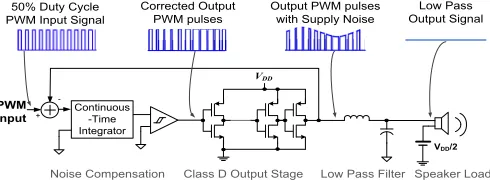
III.PWM FEEDBACK LOOP FOR HALF-BRIDGE CDA POWER STAGE
To circumvent the constraints and to meet the objectives discussed in the previous section, let us take a look at an analog PWM negative feedback loop [20] as depicted in Fig. 3. Note that this topology is very similar to the one used for self-oscillating (SO) CDAs, despite the fact that the input in this case is a PWM signal. In other words, this topology can be considered as a special case of the SO CDAs where an analog feedback mechanism is applied to the digital PWM signal. As a result, the system analysis becomes very complicated. A very detailed linearity analysis of the distortion mechanism for SO CDAs resulting from higher order loop filter had been presented in [21] and [22]. However, very little literature had reported the linearity analysis of PWM input amplifiers.
VDD
PWM
Input Continuous-Time Integrator
Noise Compensation Class D Output Stage Low Pass Filter Speaker Load Low Pass Output Signal Output PWM pulses
with Supply Noise 50% Duty Cycle
PWM Input Signal
Corrected Output PWM pulses
+
[image:2.612.51.298.314.462.2]-VDD/2
Fig. 3. CDA power stage with negative feedback.
[image:2.612.316.561.484.574.2]VDD
PWM
Input -+
C1
R1
VDD/2 R2
(a)
C1
VDD
PWM
Input -+ C2
R3
R1
VDD/2
R2
[image:3.612.50.295.57.193.2](b)
Fig. 4. A PWM CDA power stage with (a) First-Order PWM feedback loop, and (b) Second-Order PWM feedback loop.
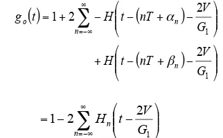
( )
!!" # $$
% &
+ = '
1
1 s KG
s s
NTFst order (2a)
( )
! ! ! !
" #
$ $ $ $
% &
+ + = '
2 1 3 2
2
2
C C RR
K s RC
K s
s s
NTFnd order (2b)
where G1 is the DC gain of the First-Order integrator (G1
=-1/(R*C1)),
K is the combined linearized gain of the quantizer and the power stage,
and
2 1
2 1
2 1
2 1 and
C C
C C C R R
R R R
+
!
= +
!
=
In general, CDA feedback systems with higher order loop filter often generate extra distortion to the overall circuit [13, 21-23]. This is either due to the DC error (for Closed-Loop system utilizing an even-order loop filter) or the phase modulation error (for Closed-Loop system utilizing an odd-order loop filter) from the high frequency ripple that affects the overall system linearity [14, 23]. In fact, this conclusion is drawn based on a Quasi-Stationary Approximation (QSA), which assumes that the audio signal is constant over one PWM cycle. Instead, a systematic time domain analysis was derived for the proposed Second-Order PWM feedback loop in [24] without any approximation to fully capture all the non-linearity in the system. The conclusion drawn from [24] are further discussed in the later part of this paper.
IV. THD ANALYSIS FOR THE PROPOSED CDA POWER STAGE
A.Mathematical analysis for First-Order PWM feedback loop
In order to enhance the THD performance of the Second-Order PWM feedback loop that was reported in [20], an investigation on the THD performance of its First-Order counterpart was first done to gain some insight into the THD performance of the general PWM feedback loop architecture. Fig. 5 depicts a Matlab Simulink model for the First-Order PWM feedback loop. A mathematical analysis is subsequently derived based on this model. Notice that the PWM input signal for this model is generated by an Open-Loop Natural Sampling PWM stage. The reason for that is to isolate any potential non-linearities generated by the PWM feedback loop
for analysis purposes. In addition, all of the signal magnitudes are normalized between the range of ±1. It is worthwhile to mention here that an adder is used in the Simulink model to obtain the difference between the input and output PWM signals instead of a subtractor because of the negative integrator gain, thus giving rise to a negative feedback system. Thereby, the integrator performs a first-order integration on the difference signal, hi(t), and the relay resembles the
hysteresis comparators in Fig. 3. In addition, the CDA output inverter stage is modeled by a simple delay for analysis purposes.
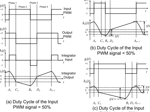
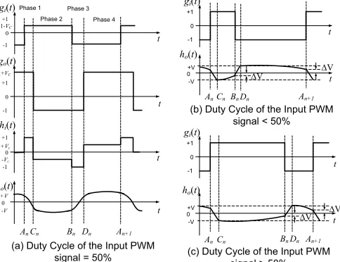
Fig. 6 depicts the time domain waveforms for one PWM cycle of the PWM feedback loop with 50% duty ratio PWM input signal. Before analyzing the signal waveform, the PWM cycle is divided into four phases. In phases 1 and 3, the input PWM signal (gi(t)) and the anti-phase output PWM signal
(go(t)) have the same magnitude, resulting in a large constant
integrator input voltage (hi(t)). Thereby, the integrator
integrates this constant voltage, resulting in a ramp at its output (ho(t)) with a gradient opposite to the polarity of hi(t)
due to the negative integrator gain. Subsequently, go(t)
switches its state once the voltage of ho(t) reaches the
threshold voltage of the hysteresis comparator, ±V, as depicted in Fig. 6. On the other hand, gi(t) and go(t) have
different voltage levels during phases 2 and 4. As a result, the resulting hi(t) is effectively zero under this condition.
Therefore, ho(t) remains at the respective threshold voltage
level until gi(t) switches state.
G1 1 s
K ++ In1 Out1
Integrator Integrator Gain
Relay
Class D Output Inverter Stage Forward Gain
K
Feedback Gain )
(t hi )
(t
gi ho(t) go(t)
Fig. 5. Matlab Simulink model of the proposed First-Order PWM feedback loop
Under noise-free conditions, go(t) should ideally be the
same as gi(t) with only a constant time delay. This can be
proven in the following by using a similar mathematical approach as in [25]
From the characteristic of the hysteresis comparator, the following relationship can be obtained:
( )
( )
! " #
< $
+ > +
=
V -en wh 1
V en
wh 1 ) (
t h
t h t
g
o o
o , (3)
where +V = upper threshold voltage level of the hysteresis comparator,
-V = lower threshold voltage level of the hysteresis comparator.
It is assumed that gi(t) is modulated from a triangular
waveform with a carrier frequency of 1/T and the switching instants of gi(t) and go(t) in Fig. 6 are denoted by (4). To
simplify the analysis, Table I summarizes the condition of
gi(t), go(t) and hi(t) for each of the time intervals between the
[image:3.612.57.300.229.389.2] [image:3.612.313.560.399.476.2](
n)
n nT
A = +! , Bn =
(
nT+!n)
,(
n)
n nT
C = +! , Dn =
(
nT+!n)
. (4) wheren is an integer,
nT+αn = an up-switching instant when gi(t) switches to +1,
nT+βn = a down-switching instant when gi(t) switches to -1,
nT+γn = a down-switching instant when go(t) switches to -1,
nT+δn = an up-switching instant when go(t) switches to +1.
Based on Fig. 5, the mathematical expression for ho(t) can be
described by the following equation:
!
"= G h t dt
t
ho() 1 i() (5) where G1 = DC gain of integrator.
To further simplify the analysis, the initial condition at the beginning of phase 1 (when t=nT+αn) for ho(t) is assumed to
be at the upper threshold voltage level, +V, of the hysteresis comparator as shown in Fig. 6. Therefore,
( )
nT h(
nT)
Vho = o +!n = (6)
With this initial condition defined in (6), equation (5) can be easily solved to obtain the following expression which describes ho(t) in phase 1.
( )
t G[
t(
nT)
]
Vho =− 1 − +
α
n + (7)As depicted in Fig. 6, the voltage level of ho(t) reaches the
lower threshold voltage level, -V, of the hysteresis comparator at the end of phase 1 (when t=nT+γn). Therefore, the final
condition for (7) is given as:
(
nT)
Vho +"n =! (8)
By substituting (8) into (7), we obtain the expression describing the timing interval between An<t<Cn.
(
) (
)
[
]
1
2 G
V A C nT
nT+#n ! +"n = n ! n = (9)
Similarly, the expression for phase 3 can be obtained using the same approach,
(
) (
)
[
]
1
2 G
V B D nT
nT+#n ! +"n = n ! n = (10)
According to [25], gi(t) and go(t) can be described as:
( )
!
"( )
#" = + =
n n
i t H t
g 1 2 (11)
( )
∑
∞( )
−∞
= + =
n n
o t H t
g 1 2 ' (12)
where Hn(t)=H(t-(nT+αn)) - H(t-(nT+βn))
H’n(t)=-H(t-(nT+γn)) + H(t-(nT+δn))
H(t) is a step function
(H(t) = 0 for t < 0 and H(t) = 1 for t > 0)
By substituting (9) and (10) into (12),
( )
(
)
(
)
⎟⎟⎠ ⎞ ⎜⎜
⎝ ⎛
−
+
−
+
⎟⎟ ⎠ ⎞ ⎜⎜
⎝ ⎛
−
+
− −
+
=
∑
∞
−∞
=
1 1
2 2 2
1
G V nT
t H
G V nT
t H t
g
n
n n
o
β α
∑
∞−∞
= ⎟⎟⎠
⎞ ⎜⎜ ⎝ ⎛
− −
=
n
n G
V t H
1
2 2
1 (13)
By comparing (11) and (13), it can be concluded that go(t)
for the First-Order PWM feedback loop is just a linear phase shifted version of gi(t) by a constant time delay of (2V/G1). In
theory, the First-Order PWM feedback loop would not generate any inherent harmonic distortion to its input reference PWM signal. Therefore, the output audio reproduction quality depends solely on the input reference PWM signal, which is a topic beyond the scope of this paper. However, it is still advisable to keep this delay to its minimum to avoid stability problems. Hence, the integrator gain of G1
should be maximized. In addition, the NTF in (2a) also suggests that the PSR performance depends heavily on both
G1 and K. Therefore, it is again advisable to keep both G1 and K as high as possible. Doing so minimizes the time delay between gi(t) and go(t) as depicted in (13). However, there are
some restrictions in maximizing G1 and K. For instance, if G1
is designed to be excessively high, ho(t) might saturate (see
Fig. 7(a)) to the positive supply rail while the integrator is trying to produce a positive slope at its output when compensating for the drop in the supply voltage level. On the other hand, if the hysteresis window width is too narrow, output pulse splitting might occur (see Fig. 7(b)) when the loop is correcting for the positive supply noise at the power stage. Due to the above mentioned constraints, a higher order integrator is imperative to further enhance the PSR performance instead of indefinitely maximizing both G1 and K.
gi(t)
hi(t)
ho(t)
t t t t +1
-1 0
+1
-1 0
+1
-1 0
+V
-V 0
Input PWM
Output PWM
Integrator Input
Integrator Output Phase 1
Phase 2 Phase 3
Phase 4
An Cn Bn Dn An+1
nT
[image:4.612.314.475.59.159.2]go(t)
[image:4.612.313.554.500.703.2]TABLE I.
INPUT CONDITIONS FOR EACH TIME INTERVAL. An < t < Cn
(Phase 1)
Cn < t < Bn
(Phase 2)
Bn < t < Dn
(Phase 3)
Dn < t < An+1
(Phase 4)
gi(t) +1 +1 -1 -1
go(t) +1 1 -1 +1
hi(t) +1 0 -1 0
ho(t) -G1[t – (n+αn)T]+V -V -G1[t – (n+βn)T] - V +V
Output PWM Signal + Noise Input PWM Signal
Correction Signal Hysteresis Windows
(b) with output pulse splitting due to narrow hysteresis window and high integrator gain (a) clipped correction signal due to large
hysteresis window and high integrator gain Clipping
Pulse Splitting
Fig. 7. Simulated waveforms for a single supply First-Order PWM feedback loop for CDA power stage
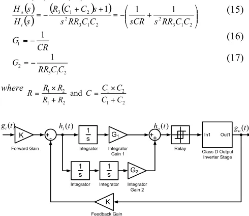
B.Causes of Inherent Harmonic Distortion for Second-Order PWM Feedback Loop
Fig. 8 depicts a Matlab Simulink model for the Second-Order PWM feedback loop. This model comprises a First-Order integrator with a gain of G1 and a Second-Order
integrator with a gain of G2. The correction signal is produced
by summing the First- and Second-Order integrator output signals. It had been shown in [20] that the THD of the Second-Order PWM feedback loop is higher than its First-Second-Order counterpart.
Equation (15) describes the transfer function of the Second-Order integrator based on Fig. 4(b). By comparing (15) to Fig. 8, the respective gain values of G1 and G2 can be identified as
shown in (16) and (17).
( )
( )
(
)
(
)
!! " # $$
% &
+
'
= + +
'
=
2 1 3 2 2
1 3 2
2 1
3 1 1 1
C C RR s sCR C
C RR s
s C C R s H
s H
i
o (15)
CR
G1=− 1 (16)
2 1 3 2
1
C C RR
G =! (17)
where
2 1
2 1
2 1
2 1 and
C C
C C C R R
R R R
+ ! = +
!
=
K +- In1 Out1
Relay
Class D Output Inverter Stage Forward Gain
K
Feedback Gain
++ G1
Integrator Gain 1
G2
Integrator Gain 2
1 s
Integrator
1 s
Integrator
1 s
Integrator ) (t hi
) (t
[image:5.612.51.534.64.283.2]gi ho(t) go(t)
Fig. 8. Matlab Simulink model of the proposed Second-Order PWM feedback Loop
Fig. 9(a) shows the time domain waveform of the
Second-Order PWM feedback loop in the absence of supply noise. Similar to the analysis for the First-Order design, ho(t) is again
divided into four phases in a single PWM cycle. However,
ho(t) no longer has a constant slope in phase 1 and 3, and a
constant voltage in phase 2 and 4 in this case. This is due to the Second-Order integrating effect on hi(t). For instance, the
constant slope in phase 1 and 3 becomes a corresponding Second-Order curve (parabola) due to the integration of a ramp signal (first-order integrated signal). Similarly, the constant value in phase 2 and 4 becomes a corresponding constant slope for the same reason.
As derived earlier, the mathematical harmonic distortion analysis for the First-Order design was relatively straight-forward. This is because the instantaneous voltage value of
ho(t) at the end of each phase is predictable and consistent
from cycle to cycle regardless of the modulation index of gi(t)
under no noise condition. In contrast, the corresponding mathematical analysis for the Second-Order model is considerably more complicated. It was explained in [21-23] that the Second-Order loop filter would always result in higher distortion than its First-Order counterpart due to the significant contribution of the DC error as a direct consequence of the ripple signal [14]. However, the approach adopted in [21-23] is based on a Quasi-Stationary Approximation, which limits the accuracy of the linearity analysis. Therefore, a very detailed and systematic mathematical analysis for the Second-Order PWM feedback loop was derived in [24] (see (18) later). This analysis proceeds in the time domain: between each switching instant of the input or output, the behavior of the amplifier is readily determined by straightforward integration. The result is a system of difference equations which are algebraic equations relating the integrator outputs sampled at time t=An+1 to the
corresponding values sampled at time t=An. The key to the
[image:5.612.56.301.482.694.2]calculation is that at no stage is any Quasi-Stationary Approximation made: at no point is it assumed that one may consider the audio signal to be effectively constant over a switching period. While such an approximation is good “at leading order”, the slight changes to the audio signal over a switching period must be accounted for in a fully systematic treatment. For a sinusoidal audio input σ(t)= σ0sin(ωt), the
audio output of the Second-Order PWM feedback loop, ga(t),
is clearly also periodic and so can be expanded as a Fourier series. In view of the symmetries of the input, σ(t)=-σ(t) and
σ(t+π/ω)=-σ(t), it is clear that only sines are needed and then only those whose angular frequencies are odd multiples of ω.
Thus ga(t) can be expanded as a Fourier sine series of odd
harmonics:
(
)
!
"=
+
+
=
0 1
2
sin
2
1
)
(
k k
a
t
G
k
t
g
#
(18)where k is a positive integer,
ω is the angular frequency of the input audio signal G1= σ0+O((ωT)2),
G2k+1= O((ωT)2),and
σ0 is the output audio magnitude.
Equation (18) shows that the original input sinusoidal signal is reproduced at the output of the Second-Order PWM feedback loop with distortion of order (ωT)2. It means that the
output harmonic distortion increases with the input audio frequency. In general, (18) provides us a detailed insight into the harmonic distortion behavior of the Second-Order design. However, it is more practical to intuitively understand the causes of harmonic distortion generated by the Second-Order feedback loop from engineering viewpoints.
Fig. 9(b) and 9(c) depict the respective output waveforms,
ho(t), of the Second-Order PWM feedback system with two
different input modulation indexes. The absolute voltage difference between ho(An) and ho(Cn) is denoted as |ΔVACn|,
and similarly, the absolute voltage difference between ho(Bn)
and ho(Dn) is denoted as |ΔVBDn|. Based on Fig. 9(b) and 9(c),
|ΔVACn| and |ΔVBDn| are to a good approximation proportional
to the modulation index of gi(t). Furthermore, the duration of
the time intervals in phase 1 and phase 3 depends heavily on the values of |ΔVACn| and |ΔVBDn|, respectively. Put differently,
the time durations of phase 1 and phase 3 vary with the duty ratio of gi(t). In contrast to the First-Order design, the time
delays in phase 1 and 3 in this case are not consistent in each PWM cycle even in the absence of supply noise. Hence, it can be safely concluded that go(t) is not an exact reproduction of gi(t) for the Second-Order PWM feedback loop. This effect is
not very obvious for gi(t) that carries low audio frequency
content. This is because the change in duty ratio between adjacent PWM cycles would be relatively small for gi(t) with
low audio frequency. Therefore, the magnitude variations of |ΔVACn| and |ΔVBDn| in the current PWM cycle compared to
those in the next PWM cycle are relatively small. However, this effect becomes more prominent in a PWM signal carrying higher audio frequency content. This is because the duty ratio changes between adjacent PWM cycles are relatively large. Therefore, the magnitude differences in |ΔVACn| and |ΔVBDn|
between adjacent PWM cycles are increased. In return, the time duration of phase 1 and phase 3 become very inconsistent.
Another potential cause of harmonic distortion comes from the pulse skipping effect of go(t). This occurs when gi(Bn) and gi(An+1) switch before ho(t) settles to its respective threshold
voltage level to trigger go(t) to switch states at Cn and Dn
respectively. For instance, the switching time sequence becomes …An, Bn, Cn,Dn… instead of ...An, Cn, Bn, Dn… under
no noise condition. This effect arises when |ΔVACn| or |ΔVBDn|
have a sufficiently high value to cause a very long integrating time in phase 1 or phase 3 respectively. In other words, potential harmonic distortion would be introduced when the system is excited by gi(t) with high modulation index. Also, it
is worth mentioning here that this effect is actually cumulative and will carry over to the next PWM cycle. Therefore, harmonic distortion due to pulse skipping is more obvious for lower audio frequency signals with large number of consecutive high duty ratio pulses.
t t t t
+1
-1 0
+1
-1 0
+1
-1 0
+V -V 0
Input PWM
Output PWM
Integrator Input
Integrator Output
Phase 1 Phase 2
Phase 3 Phase 4
gi(t)
hi(t)
ho(t)
go(t)
An Cn Bn Dn An+1
t
+V -V 0
ho(t)
t
+V -V 0
ho(t)
t
+1
-1 0
gi(t)
t
+1
-1 0
gi(t)
(b) Duty Cycle of the Input PWM signal < 50%
(c) Duty Cycle of the Input PWM signal > 50%
An CnBn An+1
AnCn BnDn
Dn
An+1
∆V
∆V
(a) Duty Cycle of the Input PWM signal = 50%
∆V
[image:6.612.317.562.291.474.2]∆V
Fig. 9. PWM input, PWM output, Integrator input and Integrator output of the Second-Order PWM feedback loop for CDA power stage without supply error.
C.Proposed THD Enhancement of the Second-Order PWM Feedback Loop
In order to alleviate the harmonic distortion problem for the Second-Order PWM feedback design, one of the options is to decrease the gain G2. Doing so reduces the maximum value of
|ΔVACn| and |ΔVBDn|, and also the tendency towards pulse
skipping as described in the previous section. Based on (15), (16) and (17), G2 can be reduced without affecting G1 by
increasing the value of R3 in Fig. 4(b). However, the zero in its
transfer function (15) would move towards the lower frequency, and eventually, a first-order roll off rate would become dominant if the value of R3 is sufficiently large. As a
result, the PSR performance would deteriorate as the NTF 2nd-Order (2b) becomes a first-order function that is equivalent to NTF1st-Order (2a). This would defeat the purpose of having a
Second-Order integrator in the correction circuit. In order to reduce the harmonic distortion while keeping its Second-Order PSR performance, a profound understanding of how |∆VACn|
As mentioned in the previous section, the huge magnitude of |ΔVACn| and |ΔVBDn| would result in a large integrating time
in phase 1 and phase 3. To minimize the delay time, the value of |∆VACn| and |∆VBDn| must be reduced. Based on the
integrator correction mechanism, |∆VACn| can be minimized by
intentionally increasing the DC magnitude (Vc) of go(t). As a
result, the integrator would attempt to correct for the intended DC error by producing a negative curve in phase 4. Thus, the maximum value of |∆VACn| would then be reduced.
Consequently, the overall integrating time in phase 1 in each PWM cycle would be reduced. However, the maximum magnitude of |∆VBDn|is not affected by simply increasing the
magnitude of go(t). Therefore, it is necessary to reduce the
magnitude of gi(t) by the same amount to produce a similar
effect in phase 2. However, the magnitude of Vc should not be
too large as it might introduce a pulse splitting problem in
go(t)similar to Fig. 7(a). In general, it is recommended that the
optimum instantaneous voltage values of ho(An) and ho(Bn)
should be near to -V and +V respectively when the system is excited by a 50% duty ratio PWM input signal under noise-free conditions as depicted in Fig. 10(a). Consequently, the resulting ho(t) would become similar to the First-Order design
in Fig. 6. This condition can be summarized as follows:
( )
+( )
= !2 1
2 1pDn k mDn
k (19)
( )
+( )
=" ! 2 12
1pCn k mCn
k (20)
In this way, the resulting time delays in phases 1 and 3 are effectively reduced. As a result, the cycle-to-cycle time delay variations are also minimized. Thereby, the overall harmonic distortion of the system is reduced. In this manner, the transfer function of the Second-Order integrator is preserved, and the overall THD of the output signal is therefore improved without compromising the Second-Order PSR performance.
t
+V -V 0
ho(t)
t
+V -V 0
ho(t)
t
+1
-1 0
gi(t)
t
+1
-1 0
gi(t)
(b) Duty Cycle of the Input PWM signal < 50%
(c) Duty Cycle of the Input PWM signal > 50% AnCn BnDn
AnCn BnDn
An+1
An+1
∆V ∆V
hi(t)
t t t +1
-1 0
+1
-1 0
+1
-1 0
+V
-V
Phase 1 Phase 2
Phase 3 Phase 4
gi(t)
go(t)
t 0
ho(t)
+1-VC
+1+VC
AnCn Bn Dn An+1
(a) Duty Cycle of the Input PWM signal = 50%
∆V
∆V
+Vc
[image:7.612.52.294.452.638.2]-Vc
Fig. 10. PWM input, PWM output, Integrator input and Integrator output of the proposed Enhanced Second-Order PWM feedback loop for CDA power stage without supply error.
In order to find the optimum Vc based on the above
mentioned criterion, the integrator output signal at each phase that was defined in [24] has to be re-defined based on Fig. 10. The re-defined equation for the integrator output signal is summarized in Table 2. Using a similar approach to that in [24] with the conditions as indicated in (19) and (20), the
equations in table 2 can be simplified to a cubic equation for
Vc as shown in (21). Therefore, the optimum value of Vc can
be easily found by solving the cubic equation (21). For example, by solving the above equation for Vc with k1
=-2666666.6667, k2=-1666666666666.67, T=250µs, and ∆=1.25,
the solutions for Vc are Vc=0.289, Vc=2.3, Vc=-1.801. Based on
simulation with both Matlab Simulink and Cadence Spectre, the optimum value of Vc to satisfy the two conditions where ho(Cn)=ho(Bn) and ho(Dn)=ho(An+1) was Vc=0.3. The negative
value of Vc is trivial and a high Vc would lead to pulse splitting
problems, which would consequently increase the PWM switching rate.
0 8 8
2 2 2 1
2 1 3 2
1V "kkTV " kV " k!=
k c c c (21)
where ∆ defines the hysteresis of the comparator
TABLE II
DEFINITION OF THE SECOND-ORDER PWM FEEDBACK LOOP OUTPUT AT DIFFERENT PHASES WITHIN ONE PWM CYCLE
An<t<Cn (phase 1)
Cn<t<Bn (phase 2)
s(t) 1-Vc 1-Vc
g(t) 1+Vc -1
hi(t) +1 -(½)Vc
m(t) m(t) = m(An) + (t-An) m(t) = m(Cn) - ½Vc(t - Cn)
p(t) p(t)= p(An) + m(An)(t - An)
+ ½(t - An)2
p(t)= p(Cn) + m(Cn)(t - Cn)
- ¼Vc(t - Cn)2
Bn<t<Dn (phase 3)
Dn<t<An+1 (phase 4)
s(t) -1 -1
g(t) -1 1+Vc
hi(t) -1 (½)Vc
m(t) m(t) = m(Bn) - (t-Bn) m(t) = m(Dn) + ½Vc(t - Dn)
p(t) p(t)= p(Bn) + m(Bn)(t - Bn)
- ½(t - Bn)2
p(t)= p(Dn) + m(Dn)(t - Dn)
+ ¼Vc(t - Dn)2
D.Proposed THD Enhancement of the Second-Order PWM Feedback Loop
Based on Fig. 4b and Fig. 8, the simplified system loop gain of the Second-Order loop is shown in (22) and the loop plot is shown in Fig. 11.
(
)
2 3
2 / 1
s C R s
loopgain= + (22)
Note that (22) contains a LHP zero at 1/(2R3C). Similar to
signal would not result in a linearity problem. In fact, this is very similar to the ripple instability condition described for the configuration B in [23]. The zero magnitude pole in the loop transfer function ensured the stability of the Closed-Loop linearized small-signal system, while the ripple instability (i.e. pulse splitting effects in this case) does not affect the Closed-Loop system linearity [23]. Instead, an extra switching in the output PWM signal improves the overall THD of the low-passed audio output signal (as the loop continues to correct the low frequency errors) at the expense of the switching power consumption and circuit reliability [23]. On the other hand, a more severe criterion for stability consideration is the pulse skipping problem as mentioned in the previous section. In the case of this Second-Order PWM feedback loop under noise-free conditions, pulse skipping occurs when the integrator gain is not sufficient to produce an output signal that is fast enough to track the PWM signal. In more serious case, oscillation occurs at the output audio signal. Therefore, the low frequency gain of the Second-Order integrator should be sufficiently high to avoid the pulse skipping problem. Hence, the system stability can be ensured.
Fig. 11. Loop gain transfer function of the optimized Second-Order PWM feedback design.
V.THD ANALYSIS FOR THE PROPOSED CDA POWER STAGE
In this section, the simulation and measurement results are presented. The First- and Second-Order designs are simulated using both Matlab Simulink Model (refer to Fig. 5 and 8) and Cadence Spectre simulation with GF’s 0.18 µm CMOS
process (refer to Fig. 4(a) and 4(b)). In addition, the proposed design was fabricated with GF’s 0.18 µm CMOS technology and the micrograph of the test chip is shown in Fig. 12. The circuit operates at 3.3V supply voltage and the maximum unclipped power efficiency obtained with a 16 Ω load condition is 89.5%. It had been shown in [20] that the proposed design attains a comparable PSR performance, with much better THD results than the PowerDac design that was introduced in [17]. In this paper, the sources of harmonic distortion of the proposed design are identified, and verified with the simulation and measurement results shown in this section.
In this section, the Second-Order feedback loop design
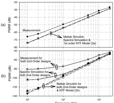
discussed in section IV part B is denoted as 2nd-Order Design. On the other hand, the Second-Order feedback loop design with Enhanced THD performance as introduced in section IV part C is denoted as Enhanced 2nd-Order Design. Fig. 13 depicts the PSR comparison of the proposed Closed-Loop CDA power stages across the audio band (from 100 Hz to 20 kHz). A 50% duty ratio PWM signal with a pulse frequency of 400 kHz was first generated by a Natural Sampling PWM modulator. A sinusoidal test tone was then applied to the positive power supply rail of the CDA power stage to simulate the supply noise condition. In addition, an ACBC-DPZ [27] op-amp was used for the integrator in both Cadence Spectre simulation and the actual chip measurement. On the basis of Fig. 13(a) and (b), the following observations are made.
1) The PSR for the proposed circuits generally degrades as the supply noise frequency increases. This is due to the high-pass noise shaping effects as shown in (2a) and (2b) 2) The slight deviation in the PSR between the simulation and measurement results is mainly due to the noise floor therein.
3) From Fig. 13(a), the PSR results for the 1st-Order design obtained from the Spectre simulation are closely matched to its Matlab Simulink Model as well as its 1st-Order NTF plot derived earlier in (2a). In addition, the simulation and the measurement results show that the 1stOrder feedback topology has a PSR of more than -60dB at 217 Hz.
4) Both of the 2nd-Order and the Enhanced 2nd-Order designs have similar PSR performance as they share the same circuit architecture and also the same NTF. 5) Fig. 13(b) shows that both the 2nd-Order design and the
Enhanced 2nd-Order design attain more than -100 dB PSR performance at 217 Hz for the simulation. However, the actual measured PSR is approximately -80 dB. 6) The deviation in the 2nd-Order NTF and the respective
Spectre simulation, and also the practical measurements, at low frequency is mainly due to the fact that the Open-Loop gain of the op-amp is not taken into account in the NTF derivation in (2b).
[image:8.612.60.262.317.474.2]In conclusion, the proposed 2nd-Order integrator feedback design architectures have a much better PSR performance across the whole audio band due to the Second-Order noise-shaping effect.
[image:8.612.394.496.563.620.2](a)
PS
R
R
(dB)
-80 -70 -60 -50 -40 -30 -20
Measurement
Matlab Simulink, Spectre Simulation & 1st order NTF Model (2a)
(b)
Frequency (Hz)
102 103 104
PS
R
R
(dB)
-140 -120 -100 -80 -60 -40
Measurement for both 2nd-Order designs
Spectre Simulation for both 2nd-Order designs
[image:9.612.57.280.62.263.2]Matlab Simulink for both 2nd-Order designs & NTF Model (2b)
Fig. 13. Comparison of PSR for the proposed power stage with (a) 1st –Order PWM feedback loop, and (b) 2nd-Order PWM feedback loop.
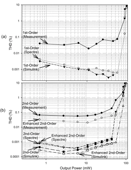
Fig. 14 depicts the THD of the Closed-Loop PWM power stages for different input modulating signal frequencies (from 100 Hz to 20 kHz). The PWM reference input of the CDA power stage is generated by modulating a sinusoidal test tone with a triangular wave carrier frequency at 400 kHz. It is worthwhile to mention here again that the PWM input signal is generated by open-loop Natural sampling PWM and the Class D power stage is implemented with zero dead time because we would like to isolate and quantify the non-linearities generated by the proposed Closed-Loop PWM power stages for analysis. On the basis of Fig. 14, the following observations are made.
1) The THD results in Fig 14(a)-(b) show that the Matlab Simulink Models are closely matched to the Spectre Simulation.
2) Based on Fig. 14(a)-(b), the simulated 1st-Order feedback loop design attains the lowest THD among the three. These results verify the earlier conclusion that no inherent THD was generated in the output PWM signal under ideal condition for the 1st-Order PWM feedback loop design.
3) From Fig. 14(b), the simulated THD results verify the analysis in section IV that the THD performance for both of the 2nd-Order and Enhanced 2nd-Order designs generally degrades as the frequency increases.
4) Following 3), the proposed Enhanced 2nd-Order Design attains a substantial improvement in THD performance across the audio band as compared to the 2nd-Order Design. In other words, it further verifies the conclusions in the THD enhancement analysis discussed in section IV, part C.
5) The measured THD is generally higher than that of the simulated results. This is mainly due to the noise floor, the quality of the LC low-pass filter, process variation, 1/f and thermal noise, power supply spike, ground bounce, substrate noise due to the high switching current, the linearity of the triangular carrier for the PWM stage, the rise and fall time of the PWM signal,
and the measuring equipment etc, that was being used in the measurement..
6) The measured THD results decrease with the input frequency because of the internal filtering effect of the measurement devices. Therefore, the harmonics of those signals with higher fundamental frequency were not captured.
(b)
Frequency (Hz)
103 104
0.001 0.01 0.1
TH
D
(
%
)
2nd-Order
(a)
TH
D
(
%
)
0.001 0.01
2nd-Order (Measurement)
Enhanced 2nd-Order (Measurement)
(Spectre)
(Measurement)
(Simulink)
Enhanced 2nd-Order (Simulink)
(Spectre)
[image:9.612.321.541.69.394.2](Simulink) (Spectre)
Figure 14. THD Performance over different input frequencies at input modulation index of 80% for (a) 1st-Order design, (b) 2nd-Order Designs
Fig. 15 depicts the THD of the three CDA power stages obtained again by Matlab Simulink, Cadence Spectre simulation, as well as practical measurement over a full output power range for 1 kHz input sinusoidal signal. The following observations are made.
1) The results obtained from the Matlab Simulink model are generally better than those obtained from the Spectre simulation and the measurement because the behavior of the actual op-amp and the process characteristics of the output power MOSFET transistors are ignored in the Matlab Simulink model.
2) Fig. 15(a) shows that the simulated THD performance for the 1st-Order design decreases as the output power increases. Conversely, the simulated THD results for both the 2nd-Order and the Enhanced 2nd-Order Designs in Fig. 15(b) increase with the output power. 3) Fig. 15(b) also depicts a relatively high simulated THD
result for the 2nd-Order Design with output power at 54 mW (the corresponding modulation index=0.9). This is mainly due to the large values of |∆VACn| and |∆VBCn|, and the pulse delay effect as explained in the earlier section.
performance at output power of 54 mW (modulation index = 0.9).
Output Power (mW)
1 10 100
T
H
D
(
%)
0.0001 0.001 0.01 0.1 1 10
2nd-Order (Measurement)
2nd-Order (Spectre)
(a)
T
H
D
(
%)
0.001 0.01 0.1 1 10
1st-Order (Spectre) 1st-Order (Measurement)
1st-Order (Simulink)
2nd-Order (Simulink)
Enhanced 2nd-Order (Spectre)
Enhanced 2nd-Order (Simulink) Enhanced 2nd-Order
(Measurement)
[image:10.612.63.279.81.362.2](b)
Figure 15. THD (%) Performance vs output power (mW) with input signal frequency of 1kHz for (a) 1st-Order design, (b) 2nd-Order Designs
As the impedance for most headphone speakers varies with frequency, it is worthwhile to investigate the performance of the proposed 1st- and 2nd-Order PWM feedback loops against the output load variations. Therefore, the resistance of the output load is reduced by approximately 4 times to investigate the non-linear effects on the system due to the reduction of the load. The cutoff freqeuncy for the respective loading condition is being maintained at 35 kHz. Fig. 16 shows the THD results across the audio band for the CDA power stages with two different loading conditions (4Ω and 16Ω).
1) As depicted by the Spectre simiulation results of the Open-Loop CDA power stage in Fig. 16(a), the THD results obtained for 4Ω resistive load is around 17 times higher than that obtained for 16Ω resistive load condition. In other words, harmonic distortion is introduced as the load resistance decreases in the Open-Loop condition.
2) Comparing the THD results of the 1st-Order design under the two loading conditions in Fig. 16(b), it can be seen that it is still relatively sensitive to the changes in the load resistance. The THD results obtained for 4Ω resistive load is approximately 14 times higher than that obtained for 16Ω resistive load condition. 3) Following 2), it was suggested by the mathematical
analysis for the 1st-Order feedback loop in the earlier section that its THD performance depends very much on the quality of the input PWM reference signal. From the simulation and measurement results, it is seen that the amount of non-linearity introduced in the
output power stage is also a factor affecting its THD performance. It is worthwhile to mention here again that the 1st-Order PWM feedback loop would not generate any inherent THD by itself.
4) Conversely, Fig. 16(c) show that the load resistance variations do not affect the THD results obtained by both the Order Design and the Enhanced 2nd-Order Design across the audio band.
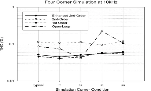
The THD performance of the proposed design against power stage transistor variations is investigated by performing the four corner simulations as depicted in Fig. 17. The worst case THD result for the Open-Loop CDA power stage is obtained in the sf condition and it deviates from the typical condition THD results by approximately 160%. In contrast, the worst case THD deviation in the four corner simulation for the 1st-Order design is below 30%, and less than 20% for both Enhanced 2nd-Order and 2nd-Order designs.
(c)
Frequency (Hz)
1000 10000
T
H
D
(
%)
0.001 0.01 0.1
2nd-Order (Measurement)
Enhanced 2nd-Order (Spectre)
2nd-Order
(Spectre) Enhanced 2nd-Order (Measurement) 4Ω
16Ω
4Ω
16Ω
16Ω
4Ω
16Ω
4Ω
(b) THD
(
%)
0.001 0.01 0.1 1
1st-Order (Measurement)
1st-Order (Spectre)
4Ω
4Ω
16Ω
16Ω
1st-Order (Spectre)
1st-Order (Measurement)
(a)
T
H
D
(
%)
0.01 0.1 1
Open-Loop (Measurement)
Open-Loop (Spectre)
4Ω
4Ω
16Ω
16Ω Open-Loop(Spectre)
[image:10.612.312.554.261.625.2]Open-Loop (Measurement)
Figure 16. THD vs Frequency plot for different load resistance, RL for (a) Open Loop CDA power stage, (b) 1st-order design (c) 2nd-order designs
only -60 dB. On the other hand, both of the proposed 2nd-Order designs achieved very good PSR measurement of -80 dB at 217 Hz and the 2nd-Order Class D power stages PWM feedback loop design is insensitive to any load variations. In addition, with careful analysis of the causes of its inherent harmonic distortion, the THD results can be reduced by at least a factor of 2. According to the Spectre simulation, the maximum THD result for the Enhanced 2nd-Order Design is less than 0.1% across the audio band and the full modulation index range. Hence, the proposed Enhanced 2nd-Order Design has the best PSR and THD trade-off over the entire range of modulation index and frequency.
Four Corner Simulation at 10kHz
Simulation Corner Condition
typical ff fs sf ss
TH
D
(%
)
0.01 0.1 1
[image:11.612.50.297.202.351.2]Enhanced 2nd-Order 2nd-Order 1st-Order Open-Loop
Figure 17. Four Corner simulation for input signal frequency of 10kHz
VI.
C
ONCLUSIONSAn in-depth mathematical analysis of the proposed First-Order feedback loop CDA power stage is presented. Also, an intuitive way to understand the causes of inherent harmonic distortion of the Second-Order feedback loop CDA power stage is provided. Based on such understanding, the harmonic distortion of the Second-Order PWM feedback loop is effectively reduced by intentionally creating a voltage difference between the input and output PWM signals. The respective behaviors of PSR and THD performance for the CDA power stage PWM feedback loop designs are verified using the Matlab Simulink Model, the Spectre Simulation, as well as practical measurement with GF’s 0.18 µm CMOS
process. The proposed Enhanced Second-Order PWM feedback loop can achieve a simulated PSR of more than −100
dB and -80 dB practically at 217 Hz, and a THD below 0.1% from 1 kHz to 20 kHz regardless of any loading condition as well as process variation. This shows that the proposed negative PWM feedback loop can effectively reduce the power supply noise and non-linearities of a CDA power stage. Hence, the power stage is very suitable for CDA applications in which the PWM signal from a digital PWM can be replicated with sufficient drive to drive the loud speaker.
VII.ACKNOWLEDGMENT
The authors would like to express their greatest appreciation to MediaTek Inc. Singapore for their support in this work.
REFERENCES
[1] K. Nielsen, "MECC - A novel control method for high end switching audio power amplification," in 105th AES Convention, San Francisco, CA, USA, preprint no. 4839, September 1998. [2] M. T. Tan, J. S. Chang, H. C. Chua, and B. H. Gwee, "An
investigation into the parameters affecting total harmonic distortion in low-voltage low-power Class-D amplifiers," IEEE Transactions on Circuits and Systems I: Fundamental Theory and Applications, vol. 50, pp. 1304-1315, 2003.
[3] L. Risbo and T. Morch, "Performance of an all-digital power amplification system," presented at the 104th AES Convention, Amsterdam, The Netherlands, May 1998.
[4] B. Putzeys, "Digital audio's final frontier," IEEE Spectrum, vol. 40, pp. 34-41, 2003.
[5] V. M. E. Antunes, V. F. Pires, and J. F. A. Silva, "Narrow Pulse Elimination PWM for Multilevel Digital Audio Power Amplifiers Using Two Cascaded H-Bridges as a Nine-Level Converter," IEEE Transactions on Power Electronics, vol. 22, pp. 425-434, 2007. [6] A. Yoneya and A. Watanabe, "Low distortion digital pulse width
modulation for audio class-D amplifier," in IEEE International Symposium on Communications and Information Technology, 2004, pp. 515-518 vol.1.
[7] C. Pascual, Z. Song, P. T. Krein, D. V. Sarwate, P. Midya, and W. J. Roeckner, "High-fidelity PWM inverter for digital audio amplification: Spectral analysis, real-time DSP implementation, and results," IEEE Transactions on Power Electronics, vol. 18, pp. 473-485, 2003.
[8] P. H. Mellor, S. P. Leigh, and B. M. G. Cheetham, "Digital sampling process for audio class D, pulse width modulated power amplifiers," Electronics Letters, vol. 28, pp. 56-58, 1992. [9] Z. Yu and H. Feng, "A method of error correction for digital class
D power amplifier," in Asia Pacific Conference on Postgraduate Research in Microelectronics & Electronics, 2009. PrimeAsia 2009. , 2009, pp. 153-156.
[10] M. Berkhout, "Class-D audio amplifiers in mobile applications," in
IEEE International Symposium on Circuits and Systems, 2009, pp. 1169-1172.
[11] S. DAVIS. (August 2005). Trends in class D amplifiers CIRRUS LOGIC AUSTIN TX.
[12] G. Pillonnet, N. Abouchi, R. Cellier, and A. Nagari, "A 0.01%THD, 70dB PSRR Single Ended Class D using variable hysteresis control for headphone amplifiers," in IEEE International Symposium on Circuits and Systems, 2009, pp. 1181-1184. [13] J. Yu, M. T. Tan, S. M. Cox, and W. L. Goh, "Time-Domain
Analysis of Intermodulation Distortion of Closed-Loop Class-D Amplifiers," IEEE Transactions on Power Electronics, vol. 27, pp. 2453-2461, 2012.
[14] L. Risbo and C. Neesgaard, "PWM Amplifier Control Loops with Minimum Aliasing Distortion," in AES 120th Convention Paris, France, May, 2006, p. 6693.
[15] P. Midya, B. Roeckner, and S. Bergstedt, "Digital correction of PWM switching amplifiers," IEEE Power Electronics Letters, vol. 2, pp. 68-72, 2004.
[16] T. Forzley and R. Mason, "A low power Class D audio amplifier with discrete time loop filter compensation," in Joint IEEE North-East Workshop on Circuits and Systems and TAISA Conference. , 2009, pp. 1-4.
[17] K. Philips, J. van den Homberg, and C. Dijkmans, "PowerDAC: a single-chip audio DAC with a 70%-efficient power stage in 0.5 µm CMOS," in IEEE International Solid-State Circuits Conference, 1999, pp. 154-155.
[18] K. Nielsen, "PEDEC-a novel pulse referenced control method for high quality digital PWM switching power amplification," in
Power Electronics Specialists Conference, 1998. PESC 98 Record. 29th Annual IEEE, 1998, pp. 200-207 vol.1.
[19] S. Logan and M. O. J. Hawksford, "Linearization of class D output stages for high-performance audio power amplifiers," in Second International Conference on Advanced A-D and D-A Conversion Techniques and their Applications, 1994, pp. 136-141.
[21] M. C. W. Høyerby and M. A. E. Andersen, "Carrier Distortion in Hysteretic Self-Oscillating Class-D Audio Power Amplifiers: Analysis and Optimization," IEEE Transactions on Power Electronics, vol. 24, pp. 714-729, 2009.
[22] J. Lu and R. Gharpurey, "Design and Analysis of a Self-Oscillating Class D Audio Amplifier Employing a Hysteretic Comparator,"
IEEE Journal of Solid-State Circuits, vol. 46, pp. 2336-2349, 2011.
[23] L. Risbo, "Discrete-time modeling of continuous-time pulse-width modulator loops," presented at the 27th Int. AES Conference, Hillerød, Denmark, September 2005.
[24] S. M. Cox, C. K. Lam, and M. T. Tan, "A second-order PWM-in/PWM-out class-D audio amplifier," IMA J. Appl. Math., June, 2011.
[25] S. M. Cox and B. H. Candy, "Class-D audio amplifiers with negative feedback," SIAM J. Appl. Math. 66, pp. 468-488, 2005. [26] R. Cellier, G. Pillonnet, N. Abouchi, R. M'Rad, and A. Nagari,
"Analysis and design of an analog control loop for digital input class D amplifiers," in IEEE International Conference on Electronics, Circuits and Systems, 2011, pp. 105-108.
[27] M. T. Tan, P. K. Chan, C. K. Lam, and C. W. Ng, "AC-Boosting Frequency Compensation with Double Pole-Zero Cancellation for Multistage Amplifiers," Circuit, Systems, and Signal Processing,


![Forecasts of the Scottish economy [November 2004]](data:image/gif;base64,R0lGODlhAQABAIAAAP///wAAACH5BAEAAAAALAAAAAABAAEAAAICRAEAOw==)