Overview
Programming Model
Cache and Bus Interface Unit Operation
Exceptions
Memory Management
Instruction Timing
Signal Descriptions
System Interface Operation
Performance Monitor
PowerPC Instruction Set Listings
Invalid Instruction Forms
PowerPC 604 Processor System Design
and Programming Considerations
Glossary
Index
2
3
4
5
6
7
8
9
A B C1
GLO INDOverview
Programming Model
Cache and Bus Interface Unit Operation
Exceptions
Memory Management
Instruction Timing
Signal Descriptions
System Interface Operation
Performance Monitor
PowerPC Instruction Set Listings
Invalid Instruction Forms
PowerPC 604 Processor System Design
and Programming Considerations
Glossary
Index
2
3
4
5
6
7
8
9
A B C1
GLO INDG522-0330-00 MPC604EUM/AD 3/98
PowerPC
™604e
RISC Microprocessor User's Manual
.
This document contains information on a new product under development. Motorola reserves the right to change or discontinue this product without notice. Information in this document is provided solely to enable system and software implementers to use PowerPC microprocessors. There are no express or implied copyright licenses granted hereunder to design or fabricate PowerPC integrated circuits or integrated circuits based on the information in this document.
The PowerPC 604e microprocessor embodies the intellectual property of IBM and of Motorola. However, neither party assumes any responsibility or liability as to any aspects of the performance, operation, or other attributes of the microprocessor as marketed by the other party. Neither party is to be considered an agent or representative of the other party, and neither has granted any right or authority to the other to assume or create any express or implied obligations on its behalf. Information such as data sheets, as well as sales terms and conditions such as prices, schedules, and support, for the microprocessor may vary as between IBM and Motorola. Accordingly, customers wishing to learn more information about the products as marketed by a given party should contact that party.
Both IBM and Motorola reserve the right to modify this manual and/or any of the products as described herein without further notice. Nothing in this manual, nor in any of the errata sheets, data sheets, and other supporting documentation, shall be interpreted as conveying an express or implied warranty, representation, or guarantee regarding the suitability of the products for any particular purpose. The parties do not assume any liability or obligation for damages of any kind arising out of the application or use of these materials. Any warranty or other obligations as to the products described herein shall be undertaken solely by the marketing party to the customer, under a separate sale agreement between the marketing party and the customer. In the absence of such an agreement, no liability is assumed by the marketing party for any damages, actual or otherwise.
“Typical” parameters can and do vary in different applications. All operating parameters, including “Typicals,” must be validated for each customer application by customer’s technical experts. Neither IBM nor Motorola convey any license under their respective intellectual property rights nor the rights of others. The products described in this manual are not designed, intended, or authorized for use as components in systems intended for surgical implant into the body, or other applications intended to support or sustain life, or for any other application in which the failure of the product could create a situation where personal injury or death may occur. Should customer purchase or use the products for any such unintended or unauthorized application, customer shall indemnify and hold IBM and Motorola and their respective officers, employees, subsidiaries, affiliates, and distributors harmless against all claims, costs, damages, and expenses, and reasonable attorney fees arising out of, directly or indirectly, any claim of personal injury or death associated with such unintended or unauthorized use, even if such claim alleges that Motorola or IBM was negligent regarding the design or manufacture of the part.
Motorola and are registered trademarks of Motorola, Inc. Motorola, Inc. is an Equal Opportunity/Affirmative Action Employer.
The PowerPC name, the PowerPC logotype, PowerPC 601, PowerPC 603, PowerPC 603e, PowerPC 604, and PowerPC 604e are trademarks of International Business Machines Corporation used by Motorola under license from International Business Machines Corporation.
© Motorola Inc. 1998. All rights reserved.
CONTENTS
Paragraph
Number Title
Page Number
About This Book
Audience ... xxiv
Organization...xxv
Suggested Reading... xxvi
General Information... xxvi
PowerPC Documentation... xxvi
Conventions ... xxviii
Acronyms and Abbreviations ... xxix
Terminology Conventions ... xxxii Chapter 1
Overview
1.1 Overview... 1-1 1.2 PowerPC 604e Microprocessor Features ... 1-2 1.3 PowerPC Architecture Implementation ... 1-8 1.3.1 Features ... 1-9 1.3.2 PowerPC 604e Processor Programming Model... 1-10 1.3.2.1 Implementation-Specific Registers... 1-10 1.3.2.2 Support for Misaligned Little-Endian Accesses ... 1-12 1.3.2.3 Instruction Set ... 1-13 1.3.3 Cache and Bus Interface Unit Operation ... 1-14 1.3.3.1 Instruction Cache ... 1-14 1.3.3.2 Data Cache... 1-15 1.3.3.3 Additional Changes to the Cache ... 1-15 1.3.4 Exceptions... 1-16 1.3.5 Memory Management... 1-21 1.3.6 Instruction Timing ... 1-21 1.3.7 Signal Descriptions ... 1-24 1.3.8 System Interface Operation ... 1-27 1.3.9 Performance Monitor ... 1-28
Chapter 2
Programming Model
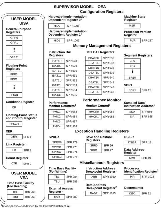
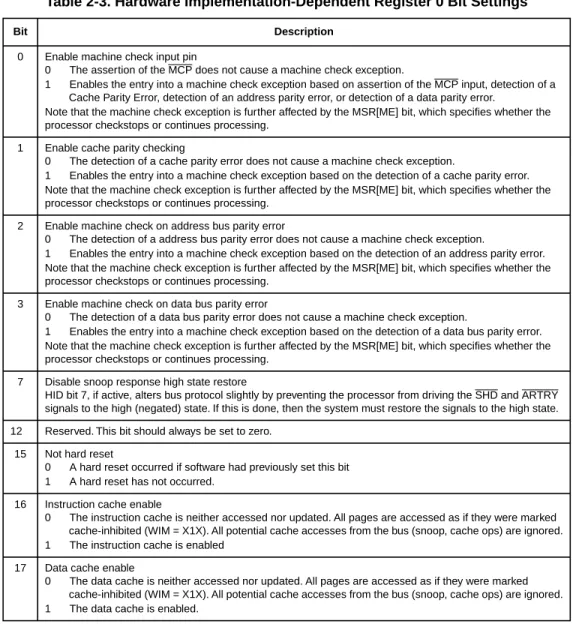
2.1 Register Set ... 2-1 2.1.1 Register Set ... 2-2 2.1.2 PowerPC 604e-Specific Registers ... 2-8 2.1.2.1 Instruction Address Breakpoint Register (IABR)... 2-9 2.1.2.2 Processor Identification Register (PIR) ... 2-9 2.1.2.3 Hardware Implementation-Dependent Register 0 ... 2-10
CONTENTS
Paragraph
Number Title
Page Number 2.1.2.4 Hardware Implementation-Dependent Register 1 (HID1) ... 2-12 2.1.2.5 Performance Monitor Registers ... 2-12 2.1.2.5.1 Monitor Mode Control Register 0 (MMCR0) ... 2-13 2.1.2.5.2 Monitor Mode Control Register 1—MMCR1... 2-14 2.1.2.5.3 Performance Monitor Counter Registers (PMC1–PMC4) ... 2-15 2.1.2.5.4 Sampled Instruction Address Register (SIA) ... 2-20 2.1.2.5.5 Sampled Data Address Register (SDA)... 2-21 2.1.3 Reset Settings... 2-21 2.2 Operand Conventions... 2-22 2.2.1 Floating-Point Execution Models—UISA... 2-22 2.2.2 Data Organization in Memory and Data Transfers... 2-23 2.2.3 Alignment and Misaligned Accesses ... 2-23 2.2.4 Support for Misaligned Little-Endian Accesses ... 2-23 2.2.5 Floating-Point Operand... 2-24 2.2.6 Effect of Operand Placement on Performance ... 2-26 2.3 Instruction Set Summary... 2-26 2.3.1 Classes of Instructions ... 2-28 2.3.1.1 Definition of Boundedly Undefined ... 2-28 2.3.1.2 Defined Instruction Class ... 2-28 2.3.1.3 Illegal Instruction Class ... 2-29 2.3.1.4 Reserved Instruction Class ... 2-30 2.3.2 Addressing Modes ... 2-30 2.3.2.1 Memory Addressing ... 2-30 2.3.2.2 Memory Operands ... 2-30 2.3.2.3 Effective Address Calculation ... 2-31 2.3.2.4 Synchronization ... 2-31 2.3.2.4.1 Context Synchronization ... 2-31 2.3.2.4.2 Execution Synchronization... 2-32 2.3.2.4.3 Instruction-Related Exceptions... 2-32 2.3.3 Instruction Set Overview ... 2-33 2.3.4 PowerPC UISA Instructions ... 2-33 2.3.4.1 Integer Instructions ... 2-33 2.3.4.1.1 Integer Arithmetic Instructions... 2-33 2.3.4.1.2 Integer Compare Instructions ... 2-35 2.3.4.1.3 Integer Logical Instructions... 2-35 2.3.4.1.4 Integer Rotate and Shift Instructions ... 2-36 2.3.4.2 Floating-Point Instructions ... 2-37 2.3.4.2.1 Floating-Point Arithmetic Instructions ... 2-37 2.3.4.2.2 Floating-Point Multiply-Add Instructions ... 2-38 2.3.4.2.3 Floating-Point Rounding and Conversion Instructions ... 2-38 2.3.4.2.4 Floating-Point Compare Instructions... 2-39 2.3.4.2.5 Floating-Point Status and Control Register Instructions ... 2-39 2.3.4.2.6 Floating-Point Move Instructions ... 2-40
CONTENTS
Paragraph
Number Title
Page Number 2.3.4.3 Load and Store Instructions ... 2-40 2.3.4.3.1 Self-Modifying Code ... 2-41 2.3.4.3.2 Integer Load and Store Address Generation... 2-41 2.3.4.3.3 Register Indirect Integer Load Instructions ... 2-42 2.3.4.3.4 Integer Store Instructions... 2-43 2.3.4.3.5 Integer Load and Store with Byte Reverse Instructions ... 2-44 2.3.4.3.6 Integer Load and Store Multiple Instructions... 2-44 2.3.4.3.7 Integer Load and Store String Instructions... 2-45 2.3.4.3.8 Floating-Point Load and Store Address Generation... 2-47 2.3.4.3.9 Floating-Point Store Instructions... 2-48 2.3.4.4 Branch and Flow Control Instructions... 2-50 2.3.4.4.1 Branch Instruction Address Calculation... 2-50 2.3.4.4.2 Branch Instructions... 2-50 2.3.4.4.3 Condition Register Logical Instructions... 2-51 2.3.4.4.4 Trap Instructions... 2-51 2.3.4.5 System Linkage Instruction—UISA... 2-52 2.3.4.6 Processor Control Instructions—UISA ... 2-52 2.3.4.6.1 Move to/from Condition Register Instructions... 2-52 2.3.4.6.2 Move to/from Special-Purpose Register Instructions (UISA)... 2-53 2.3.4.7 Memory Synchronization Instructions—UISA ... 2-53 2.3.5 PowerPC VEA Instructions ... 2-54 2.3.5.1 Processor Control Instructions—VEA ... 2-55 2.3.5.2 Memory Synchronization Instructions—VEA ... 2-55 2.3.5.3 Memory Control Instructions—VEA ... 2-56 2.3.5.3.1 User-Level Cache Instructions—VEA ... 2-57 2.3.5.4 Optional External Control Instructions... 2-59 2.3.6 PowerPC OEA Instructions ... 2-59 2.3.6.1 System Linkage Instructions—OEA ... 2-59 2.3.6.2 Processor Control Instructions—OEA ... 2-59 2.3.6.3 Memory Control Instructions—OEA ... 2-61 2.3.6.3.1 Supervisor-Level Cache Management Instruction—(OEA) ... 2-61 2.3.6.3.2 Segment Register Manipulation Instructions (OEA)... 2-61 2.3.6.3.3 Translation Lookaside Buffer Management Instructions—(OEA) ... 2-62 2.3.7 Recommended Simplified Mnemonics... 2-63
Chapter 3
Cache and Bus Interface Unit Operation
3.1 Data Cache Organization ... 3-4 3.2 Instruction Cache Organization ... 3-5 3.3 MMUs/Bus Interface Unit ... 3-6 3.4 Memory Coherency Actions ... 3-9
CONTENTS
Paragraph
Number Title
Page Number 3.4.1 PowerPC 604e-Initiated Load and Store Operations ... 3-9 3.4.2 General Comments on Snooping ... 3-10 3.5 Sequential Consistency ... 3-11 3.5.1 Sequential Consistency Within a Single Processor ... 3-11 3.5.2 Weak Consistency between Multiple Processors ... 3-11 3.5.3 Sequential Consistency Within Multiprocessor Systems ... 3-12 3.6 Memory and Cache Coherency... 3-12 3.6.1 Data Cache Coherency Protocol ... 3-13 3.6.2 Coherency and Secondary Caches ... 3-15 3.6.3 Page Table Control Bits ... 3-15 3.6.4 MESI State Diagram ... 3-15 3.6.5 Coherency Paradoxes in Single-Processor Systems ... 3-16 3.6.6 Coherency Paradoxes in Multiple-Processor Systems... 3-17 3.7 Cache Configuration ... 3-17 3.8 Cache Control Instructions ... 3-18 3.8.1 Instruction Cache Block Invalidate (icbi)... 3-18 3.8.2 Instruction Synchronize (isync)... 3-19 3.8.3 Data Cache Block Touch (dcbt) and Data Cache Block Touch
for Store (dcbtst) ... 3-19 3.8.4 Data Cache Block Set to Zero (dcbz) ... 3-19 3.8.5 Data Cache Block Store (dcbst) ... 3-20 3.8.6 Data Cache Block Flush (dcbf) ... 3-20 3.8.7 Data Cache Block Invalidate (dcbi) ... 3-20 3.9 Basic Cache Operations ... 3-20 3.9.1 Cache Reloads... 3-20 3.9.2 Cache Cast-Out Operation ... 3-21 3.9.3 Cache Block Push Operation ... 3-21 3.9.4 Atomic Memory References ... 3-21 3.9.5 Snoop Response to Bus Operations ... 3-22 3.9.6 Cache Reaction to Specific Bus Operations ... 3-22 3.9.7 Enveloped High-Priority Cache Block Push Operation ... 3-25 3.9.8 Bus Operations Caused by Cache Control Instructions... 3-26 3.9.9 Cache Control Instructions ... 3-26 3.10 Cache Actions ... 3-27 3.11 Access to Direct-Store Segments... 3-48
Chapter 4
Exceptions
4.1 PowerPC 604e Microprocessor Exceptions... 4-2 4.2 Exception Recognition and Priorities ... 4-5 4.3 Exception Processing ... 4-6 4.3.1 Enabling and Disabling Exceptions ... 4-9
CONTENTS
Paragraph
Number Title
Page Number 4.3.2 Steps for Exception Processing... 4-10 4.3.3 Setting MSR[RI] ... 4-11 4.3.4 Returning from an Exception Handler... 4-11 4.4 Process Switching ... 4-11 4.5 Exception Definitions ... 4-12 4.5.1 System Reset Exception (0x00100) ... 4-13 4.5.2 Machine Check Exception (0x00200) ... 4-14 4.5.2.1 Machine Check Exception Enabled (MSR[ME] = 1)... 4-15 4.5.2.2 Checkstop State (MSR[ME] = 0) ... 4-16 4.5.3 DSI Exception (0x00300) ... 4-16 4.5.4 ISI Exception (0x00400)... 4-16 4.5.5 External Interrupt Exception (0x00500) ... 4-16 4.5.6 Alignment Exception (0x00600) ... 4-17 4.5.7 Program Exception (0x00700)... 4-18 4.5.8 Floating-Point Unavailable Exception (0x00800) ... 4-19 4.5.9 Decrementer Exception (0x00900) ... 4-19 4.5.10 System Call Exception (0x00C00) ... 4-19 4.5.11 Trace Exception (0x00D00)... 4-19 4.5.12 Floating-Point Assist Exception (0x00E00) ... 4-20 4.5.13 Performance Monitoring Interrupt (0x00F00) ... 4-20 4.5.14 Instruction Address Breakpoint Exception (0x01300) ... 4-21 4.5.15 System Management Interrupt (0x01400) ... 4-21 4.5.16 Power Management ... 4-21 Chapter 5 Memory Management 5.1 MMU Overview... 5-2 5.1.1 Memory Addressing ... 5-4 5.1.2 MMU Organization... 5-4 5.1.3 Address Translation Mechanisms ... 5-9 5.1.4 Memory Protection Facilities... 5-11 5.1.5 Page History Information... 5-12 5.1.6 General Flow of MMU Address Translation ... 5-12 5.1.6.1 Real Addressing Mode and Block Address Translation Selection ... 5-12 5.1.6.2 Page and Direct-Store Interface Address Translation Selection... 5-14 5.1.6.2.1 Selection of Page Address Translation ... 5-16 5.1.6.2.2 Selection of Direct-Store Interface Address Translation... 5-16 5.1.7 MMU Exceptions Summary ... 5-16 5.1.8 MMU Instructions and Register Summary ... 5-18 5.1.9 TLB Entry Invalidation... 5-20 5.2 Real Addressing Mode... 5-20
CONTENTS
Paragraph
Number Title
Page Number 5.3 Block Address Translation... 5-20 5.4 Memory Segment Model ... 5-20 5.4.1 Page History Recording ... 5-21 5.4.1.1 Referenced Bit ... 5-22 5.4.1.2 Changed Bit ... 5-22 5.4.1.3 Scenarios for Referenced and Changed Bit Recording ... 5-23 5.4.2 Page Memory Protection ... 5-24 5.4.3 TLB Description ... 5-24 5.4.3.1 TLB Organization ... 5-25 5.4.3.2 TLB Invalidation ... 5-26 5.4.4 Page Address Translation Summary... 5-28 5.4.5 Page Table Search Operation... 5-30 5.4.6 Page Table Updates ... 5-34 5.4.7 Segment Register Updates ... 5-35 5.5 Direct-Store Interface Address Translation ... 5-35 5.5.1 Direct-Store Interface Accesses... 5-35 5.5.2 Direct-Store Segment Protection ... 5-36 5.5.3 Instructions Not Supported in Direct-Store Segments... 5-36 5.5.4 Instructions with No Effect in Direct-Store Segments ... 5-36 5.5.5 Direct-Store Segment Translation Summary Flow... 5-37
Chapter 6
Instruction Timing
6.1 Terminology and Conventions... 6-1 6.2 Instruction Timing Overview... 6-3 6.2.1 Pipeline Structures ... 6-5 6.2.1.1 Description of Pipeline Stages... 6-7 6.2.1.1.1 Fetch Stage ... 6-8 6.2.1.1.2 Decode Stage ... 6-8 6.2.1.1.3 Dispatch Stage ... 6-9 6.2.1.1.4 Execute Stage ... 6-9 6.2.1.1.5 Complete Stage... 6-10 6.2.1.1.6 Write-Back Stage... 6-11 6.3 Memory Performance Considerations ... 6-11 6.3.1 MMU Overview... 6-12 6.3.2 Cache Overview... 6-12 6.3.3 Bus Interface Overview ... 6-14 6.3.4 Memory Operations ... 6-14 6.3.4.1 Write-Back Mode ... 6-14 6.3.4.2 Write-Through Mode... 6-15 6.3.4.3 Cache-Inhibited Mode ... 6-15 6.4 Timing Considerations... 6-16
CONTENTS
Paragraph
Number Title
Page Number 6.4.1 General Instruction Flow ... 6-16 6.4.2 Instruction Fetch Timing ... 6-17 6.4.2.1 Cache Hit Timing Example ... 6-17 6.4.2.2 Cache Miss Timing Example... 6-21 6.4.3 Cache Arbitration... 6-23 6.4.4 Branch Prediction ... 6-23 6.4.4.1 Branch Timing Examples ... 6-24 6.4.4.1.1 Timing Example—Branch Timing for a BTAC Hit... 6-24 6.4.4.1.2 Timing Example—Branch with BTAC Miss/Decode Correction... 6-25 6.4.4.1.3 Timing Example—Branch with BTAC Miss/Dispatch Correction... 6-27 6.4.4.1.4 Timing Example—Branch with BTAC Miss/Execute Correction ... 6-27 6.4.5 Speculative Execution... 6-28 6.4.6 Instruction Dispatch and Completion Considerations ... 6-29 6.4.6.1 Rename Register Operation ... 6-30 6.4.6.2 Execution Unit Considerations ... 6-32 6.4.7 Instruction Serialization ... 6-32 6.4.7.1 Dispatch Serialization Mode... 6-33 6.4.7.2 Execution Serialization Mode... 6-33 6.4.7.3 Postdispatch Serialization Mode... 6-33 6.4.7.4 Serialization of String/Multiple Instructions ... 6-34 6.4.7.5 Serialization of Input/Output ... 6-34 6.5 Execution Unit Timings... 6-34 6.5.1 Branch Unit Instruction Timings ... 6-34 6.5.2 Integer Unit Instruction Timings ... 6-34 6.5.3 Floating-Point Unit Instruction Timings... 6-36 6.5.4 Load/Store Unit Instruction Timings ... 6-38 6.5.5 isync, rfi, and sc Instruction Timings... 6-40 6.6 Instruction Scheduling Guidelines... 6-41 6.6.1 Instruction Dispatch Rules... 6-41 6.6.2 Additional Programming Tips for the PowerPC 604e Processor ... 6-42 6.7 Instruction Latency Summary... 6-44
Chapter 7
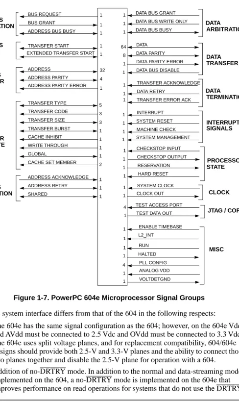
Signal Descriptions
7.1 Signal Configuration... 7-2 7.2 Signal Descriptions ... 7-3 7.2.1 Address Bus Arbitration Signals... 7-4 7.2.1.1 Bus Request (BR)—Output ... 7-4 7.2.1.2 Bus Grant (BG)—Input ... 7-4 7.2.1.3 Address Bus Busy (ABB) ... 7-5 7.2.1.3.1 Address Bus Busy (ABB)—Output... 7-5
CONTENTS
Paragraph
Number Title
Page Number 7.2.1.3.2 Address Bus Busy (ABB)—Input ... 7-5 7.2.2 Address Transfer Start Signals ... 7-6 7.2.2.1 Transfer Start (TS) ... 7-6 7.2.2.1.1 Transfer Start (TS)—Output... 7-6 7.2.2.1.2 Transfer Start (TS)—Input ... 7-6 7.2.2.2 Extended Address Transfer Start (XATS) ... 7-7 7.2.2.2.1 Extended Address Transfer Start (XATS)—Output... 7-7 7.2.2.2.2 Extended Address Transfer Start (XATS)—Input ... 7-7 7.2.3 Address Transfer Signals ... 7-7 7.2.3.1 Address Bus (A[0–31])... 7-8 7.2.3.1.1 Address Bus (A[0–31])—Output (Memory Operations)... 7-8 7.2.3.1.2 Address Bus (A[0–31])—Input (Memory Operations) ... 7-8 7.2.3.1.3 Address Bus (A[0–31])—Output (Direct-Store Operations)... 7-8 7.2.3.1.4 Address Bus (A[0–31])—Input (Direct-Store Operations) ... 7-9 7.2.3.2 Address Bus Parity (AP[0–3]) ... 7-9 7.2.3.2.1 Address Bus Parity (AP[0–3])—Output... 7-9 7.2.3.2.2 Address Bus Parity (AP[0–3])—Input... 7-9 7.2.3.3 Address Parity Error (APE)—Output ... 7-10 7.2.4 Address Transfer Attribute Signals... 7-10 7.2.4.1 Transfer Type (TT[0–4]) ... 7-10 7.2.4.1.1 Transfer Type (TT[0–4])—Output ... 7-10 7.2.4.1.2 Transfer Type (TT[0–4])—Input... 7-11 7.2.4.2 Transfer Size (TSIZ[0–2]) ... 7-12 7.2.4.2.1 Transfer Size (TSIZ[0–2])—Output ... 7-12 7.2.4.2.2 Transfer Size (TSIZ[0–2])—Input... 7-13 7.2.4.3 Transfer Burst (TBST)... 7-13 7.2.4.3.1 Transfer Burst (TBST)—Output... 7-13 7.2.4.3.2 Transfer Burst (TBST)—Input ... 7-14 7.2.4.4 Transfer Code (TC[0–2])—Output... 7-14 7.2.4.5 Cache Inhibit (CI)—Output ... 7-17 7.2.4.6 Write-Through (WT)—Output ... 7-17 7.2.4.7 Global (GBL)... 7-18 7.2.4.7.1 Global (GBL)—Output... 7-18 7.2.4.7.2 Global (GBL)—Input ... 7-18 7.2.4.8 Cache Set Element (CSE[0–1])—Output ... 7-18 7.2.5 Address Transfer Termination Signals ... 7-18 7.2.5.1 Address Acknowledge (AACK)—Input... 7-18 7.2.5.2 Address Retry (ARTRY) ... 7-19 7.2.5.2.1 Address Retry (ARTRY)—Output ... 7-19 7.2.5.2.2 Address Retry (ARTRY)—Input... 7-20 7.2.5.3 Shared (SHD)... 7-20 7.2.5.3.1 Shared (SHD)—Output ... 7-20 7.2.5.3.2 Shared (SHD)—Input ... 7-21
CONTENTS
Paragraph
Number Title
Page Number 7.2.6 Data Bus Arbitration Signals ... 7-21 7.2.6.1 Data Bus Grant (DBG)—Input ... 7-21 7.2.6.2 Data Bus Write Only (DBWO)—Input ... 7-22 7.2.6.3 Data Bus Busy (DBB) ... 7-22 7.2.6.3.1 Data Bus Busy (DBB)—Output ... 7-22 7.2.6.3.2 Data Bus Busy (DBB)—Input ... 7-23 7.2.7 Data Transfer Signals... 7-23 7.2.7.1 Data Bus (DH[0–31], DL[0–31]) ... 7-23 7.2.7.1.1 Data Bus (DH[0–31], DL[0–31])—Output ... 7-24 7.2.7.1.2 Data Bus (DH[0–31], DL[0–31])—Input ... 7-24 7.2.7.2 Data Bus Parity (DP[0–7])... 7-24 7.2.7.2.1 Data Bus Parity (DP[0–7])—Output ... 7-24 7.2.7.2.2 Data Bus Parity (DP[0–7])—Input ... 7-25 7.2.7.3 Data Parity Error (DPE)—Output ... 7-25 7.2.7.4 Data Bus Disable (DBDIS)—Input ... 7-26 7.2.8 Data Transfer Termination Signals... 7-26 7.2.8.1 Transfer Acknowledge (TA)—Input ... 7-26 7.2.8.2 Data Retry (DRTRY)—Input ... 7-27 7.2.8.3 Transfer Error Acknowledge (TEA)—Input ... 7-27 7.2.9 System Interrupt, Checkstop, and Reset Signals ... 7-28 7.2.9.1 Interrupt (INT)—Input... 7-28 7.2.9.2 System Management Interrupt (SMI)—Input ... 7-29 7.2.9.3 Machine Check Interrupt (MCP)—Input... 7-29 7.2.9.4 Checkstop Input(CKSTP_IN)—Input ... 7-30 7.2.9.5 Checkstop Output (CKSTP_OUT)—Output ... 7-30 7.2.9.6 Reset Signals... 7-30 7.2.9.6.1 Hard Reset (HRESET)—Input ... 7-30 7.2.9.6.2 Soft Reset (SRESET)—Input ... 7-31 7.2.10 Processor Configuration Signals... 7-31 7.2.10.1 Drive Mode (DRVMOD)—Input ... 7-31 7.2.10.2 Timebase Enable (TBEN)—Input ... 7-31 7.2.10.3 Reservation (RSRV)—Output ... 7-32 7.2.10.4 L2 Intervention (L2_INT)—Input ... 7-32 7.2.10.5 Run (RUN)—Input ... 7-32 7.2.10.6 Halted (HALTED) —Output ... 7-33 7.2.11 COP/Scan Interface... 7-33 7.2.12 Clock Signals ... 7-34 7.2.13 Power Management ... 7-34 7.2.13.1 State Transition from Normal Mode to Doze Mode... 7-35 7.2.13.2 State Transition from Doze Mode to Nap Mode ... 7-35 7.2.13.3 State Transition from Nap Mode to Doze Mode ... 7-35 7.2.13.4 State Transition from Nap Mode to Normal Mode ... 7-35
CONTENTS
Paragraph
Number Title
Page Number 7.2.13.6 System Clock (SYSCLK)—Input... 7-36 7.2.13.7 Test Clock (CLK_OUT)—Output ... 7-36 7.2.14 Analog VDD (AVDD)—Input ... 7-37 7.2.15 VOLTDETGND Signal (BGA Package Only)... 7-37 7.2.16 PLL Configuration (PLL_CFG[0–3])—Input ... 7-37
Chapter 8
System Interface Operation
8.1 Overview... 8-1 8.1.1 Operation of the Instruction and Data Caches ... 8-2 8.1.2 Operation of the System Interface ... 8-4 8.1.3 Direct-Store Accesses ... 8-5 8.2 Memory Access Protocol... 8-6 8.2.1 Arbitration Signals ... 8-7 8.2.2 Address Pipelining and Split-Bus Transactions... 8-9 8.3 Address Bus Tenure... 8-10 8.3.1 Address Bus Arbitration ... 8-10 8.3.2 Address Transfer... 8-12 8.3.2.1 Address Bus Parity ... 8-13 8.3.2.2 Address Transfer Attribute Signals ... 8-13 8.3.2.2.1 Transfer Type (TT[0–4]) Signals... 8-14 8.3.2.2.2 Transfer Size (TSIZ[0–2]) Signals ... 8-14 8.3.2.3 Burst Ordering During Data Transfers ... 8-14 8.3.2.4 Effect of Alignment in Data Transfers ... 8-15 8.3.2.4.1 Alignment of External Control Instructions ... 8-17 8.3.2.5 Transfer Code (TC[0–2]) Signals ... 8-18 8.3.3 Address Transfer Termination ... 8-19 8.4 Data Bus Tenure ... 8-20 8.4.1 Data Bus Arbitration ... 8-21 8.4.1.1 Effect of ARTRY Assertion on Data Transfer and Arbitration... 8-22 8.4.1.2 Using the DBB Signal ... 8-23 8.4.2 Data Bus Write Only... 8-24 8.4.3 Data Transfer ... 8-24 8.4.4 Data Transfer Termination... 8-25 8.4.4.1 Normal Single-Beat Termination ... 8-26 8.4.4.2 Data Transfer Termination Due to a Bus Error ... 8-29 8.4.5 Memory Coherency—MESI Protocol ... 8-30 8.5 Timing Examples ... 8-33 8.6 Direct-Store Operation... 8-39 8.6.1 Direct-Store Transactions ... 8-41 8.6.1.1 Store Operations ... 8-42 8.6.1.2 Load Operations... 8-42
CONTENTS
Paragraph
Number Title
Page Number 8.6.2 Direct-Store Transaction Protocol Details ... 8-43 8.6.2.1 Packet 0... 8-44 8.6.2.2 Packet 1... 8-45 8.6.3 I/O Reply Operations ... 8-45 8.6.4 Direct-Store Operation Timing ... 8-47 8.7 Optional Bus Configurations ... 8-49 8.7.1 Data Streaming Mode ... 8-49 8.7.1.1 Data Streaming Mode Design Considerations... 8-51 8.7.1.2 Data Streaming in the Data Streaming Mode ... 8-51 8.7.1.3 Data Bus Arbitration in Data Streaming Mode ... 8-52 8.7.1.4 Data Valid Window in the Data Streaming Mode... 8-52 8.7.2 No-DRTRY Mode ... 8-53 8.8 Interrupt, Checkstop, and Reset Signals ... 8-54 8.8.1 External Interrupts ... 8-54 8.8.2 Checkstops ... 8-54 8.8.3 Reset Inputs... 8-54 8.8.4 PowerPC 604e Processor Configuration during HRESET ... 8-54 8.9 Processor State Signals ... 8-55 8.9.1 Support for the lwarx/stwcx. Instruction Pair ... 8-55 8.10 IEEE 1149.1-Compliant Interface ... 8-55 8.10.1 IEEE 1149.1 Interface Description ... 8-55 8.11 Using Data Bus Write Only ... 8-56
Chapter 9
Performance Monitor
9.1 Performance Monitor Interrupt ... 9-2 9.1.1 Special-Purpose Registers Used by Performance Monitor... 9-2 9.1.1.1 Performance Monitor Counter Registers (PMC1–PMC4) ... 9-3 9.1.1.2 SIA and SDA Registers ... 9-9 9.1.1.2.1 Sampled Instruction Address Register (SIA) ... 9-9 9.1.1.2.2 Sampled Data Address Register (SDA)... 9-9 9.1.1.2.3 Updating SIA and SDA ... 9-10 9.1.1.3 Monitor Mode Control Register 0 (MMCR0) ... 9-10 9.1.1.3.1 Monitor Mode Control Register 1—MMCR1... 9-12 9.1.2 Event Counting ... 9-12 9.1.2.1 Event Selection ... 9-13 9.1.2.2 Threshold Events ... 9-13 9.1.2.2.1 Threshold Conditions ... 9-14 9.1.2.2.2 Lateral L2 Cache Intervention ... 9-14 9.1.2.2.3 Warnings... 9-14 9.1.2.3 Nonthreshold Events... 9-15
CONTENTS
Paragraph
Number Title
Page Number
ILLUSTRATIONS
Figure Number Title Page Number 1-1 Block Diagram... 1-3 1-2 Programming Model—PowerPC 604e Microprocessor Registers ... 1-11 1-3 Big-Endian and Little-Endian Memory Mapping ... 1-13 1-4 Cache Unit Organization ... 1-14 1-5 Pipeline Diagram ... 1-21 1-6 Block Diagram—Internal Data Paths ... 1-23 1-7 PowerPC 604e Microprocessor Signal Groups ... 1-25 1-8 System Interface ... 1-27 2-1 Programming Model—PowerPC 604e Microprocessor Registers ... 2-3 2-2 Instruction Address Breakpoint Register... 2-9 2-3 Processor Identification Register... 2-9 2-4 HID1 Clock Configuration Register... 2-12 2-5 Monitor Mode Control Register 1 (MMCR1) ... 2-14 2-6 Big-Endian and Little-Endian Memory Mapping ... 2-24 3-1 Cache Unit Organization ... 3-3 3-2 Cache Integration... 3-4 3-3 Bus Interface Unit and MMU ... 3-7 3-4 Memory Queue Organization ... 3-8 3-5 MESI States ... 3-14 3-6 MESI Cache Coherency Protocol—State Diagram (WIM = 001) ... 3-16 4-1 Machine Status Save/Restore Register 0 ... 4-6 4-2 Machine Status Save/Restore Register 1 ... 4-6 4-3 Machine State Register (MSR)... 4-7 5-1 MMU Conceptual Block Diagram—32-Bit Implementations ... 5-6 5-2 PowerPC 604e Microprocessor IMMU Block Diagram ... 5-7 5-3 PowerPC 604e Microprocessor DMMU Block Diagram... 5-8 5-4 Address Translation Types ... 5-10 5-5 General Flow of Address Translation (Real Addressing Mode and Block)... 5-13 5-6 General Flow of Page and Direct-Store Interface Address Translation ... 5-15 5-7 Segment Register and DTLB Organization... 5-25 5-8 Page Address Translation Flow—TLB Hit ... 5-29 5-9 Primary Page Table Search... 5-32 5-10 Secondary Page Table Search Flow ... 5-33 5-11 Direct-Store Segment Translation Flow ... 5-37 6-1 Block Diagram—Internal Data Paths ... 6-4 6-2 GPR Reservation Stations and Result Buses ... 6-5 6-3 Pipeline Diagram ... 6-6 6-4 PowerPC 604e Microprocessor Pipeline Stages... 6-7 6-5 Data Caches and Memory Queues... 6-13 6-6 Instruction Timing—Cache Hit ... 6-18 6-7 Instruction Timing—Instruction Cache Miss (BTAC Hit)... 6-21 6-8 Instruction Timing—Branch with BTAC Hit... 6-24ILLUSTRATIONS
Figure
Number Title
Page Number 6-10 Instruction Timing—Branch with BTAC Miss/Dispatch Correction... 6-27 6-11 Instruction Timing—Branch with BTAC Miss/Execute Correction ... 6-28 6-12 GPR Rename Register ... 6-31 6-13 SCIU Block Diagram... 6-35 6-14 MCIU Block Diagram ... 6-36 6-15 FPU Block Diagram ... 6-37 6-16 LSU Block Diagram ... 6-39 6-17 Store Queue Structure... 6-40 7-1 Signal Groups ... 7-3 7-2 IEEE 1149.1-Compliant Boundary Scan Interface... 7-33 7-3 Power Management States... 7-34 8-1 Block Diagram... 8-3 8-2 Timing Diagram Legend ... 8-5 8-3 Overlapping Tenures on the Bus for a Single-Beat Transfer ... 8-6 8-4 Address Bus Arbitration ... 8-10 8-5 Address Bus Arbitration Showing Bus Parking ... 8-11 8-6 Address Bus Transfer ... 8-13 8-7 Snooped Address Cycle with ARTRY ... 8-20 8-8 Data Bus Arbitration... 8-21 8-9 Qualified DBG Generation Following ARTRY ... 8-23 8-10 Normal Single-Beat Read Termination ... 8-26 8-11 Normal Single-Beat Write Termination ... 8-27 8-12 Normal Burst Transaction ... 8-27 8-13 Termination with DRTRY... 8-28 8-14 Read Burst with TA Wait States and DRTRY ... 8-29 8-15 MESI Cache Coherency Protocol—State Diagram (WIM = 001) ... 8-32 8-16 Fastest Single-Beat Reads ... 8-33 8-17 Fastest Single-Beat Writes... 8-34 8-18 Single-Beat Reads Showing Data-Delay Controls ... 8-35 8-19 Single-Beat Writes Showing Data Delay Controls... 8-36 8-20 Burst Transfers with Data Delay Controls ... 8-37 8-21 Use of Transfer Error Acknowledge (TEA) ... 8-38 8-22 Direct-Store Tenures... 8-41 8-23 Direct-Store Operation—Packet 0... 8-44 8-24 Direct-Store Operation—Packet 1... 8-45 8-25 I/O Reply Operation ... 8-46 8-26 Direct-Store Interface Load Access Example... 8-48 8-27 Direct-Store Interface Store Access Example ... 8-49 8-28 Data Transfer in Fast-L2/Data Streaming Mode ... 8-52 8-29 Data Bus Write Only Transaction ... 8-57 9-1 Monitor Mode Control Register 1 (MMCR1) ... 9-12
TABLES
Table
Number Title
Page Number i Acronyms and Abbreviated Terms ... xxix ii Terminology Conventions ... xxxii iii Instruction Field Conventions ... xxxiii 1-1 Exception Classifications ... 1-18 1-2 Overview of Exceptions and Conditions ... 1-18 2-1 MSR[PM] Bit... 2-6 2-2 Instruction Address Breakpoint Register Bit Settings ... 2-9 2-3 Hardware Implementation-Dependent Register 0 Bit Settings ... 2-10 2-4 HID1 Bit Settings... 2-12 2-5 MMCR0 Bit Settings ... 2-13 2-6 MMCR1 Bit Settings ... 2-15 2-7 Selectable Events—PMC1 ... 2-15 2-8 Selectable Events—PMC2 ... 2-17 2-9 Selectable Events—PMC3 ... 2-18 2-10 Selectable Events—PMC4 ... 2-19 2-11 Settings after Hard Reset (Used at Power-On) ... 2-21 2-12 Floating-Point Operand Data Type Behavior ... 2-25 2-13 Floating-Point Result Data Type Behavior ... 2-26 2-14 Integer Arithmetic Instructions ... 2-33 2-15 Integer Compare Instructions... 2-35 2-16 Integer Logical Instructions ... 2-35 2-17 Integer Rotate Instructions ... 2-36 2-18 Integer Shift Instructions ... 2-37 2-19 Floating-Point Arithmetic Instructions ... 2-37 2-20 Floating-Point Multiply-Add Instructions ... 2-38 2-21 Floating-Point Rounding and Conversion Instructions ... 2-39 2-22 Floating-Point Compare Instructions... 2-39 2-23 Floating-Point Status and Control Register Instructions ... 2-39 2-24 Floating-Point Move Instructions ... 2-40 2-25 Integer Load Instructions ... 2-42 2-26 Integer Store Instructions ... 2-43 2-27 Integer Load and Store with Byte Reverse Instructions ... 2-44 2-28 Integer Load and Store Multiple Instructions ... 2-45 2-29 Integer Load and Store String Instructions ... 2-46 2-30 Floating-Point Load Instructions ... 2-47 2-31 Floating-Point Store Instructions ... 2-48 2-32 Store Floating-Point Single Behavior ... 2-48 2-33 Store Floating-Point Double Behavior ... 2-49 2-34 Branch Instructions ... 2-51 2-35 Condition Register Logical Instructions ... 2-51 2-36 Trap Instructions ... 2-51 2-37 System Linkage Instruction—UISA ... 2-52
TABLES
Table
Number Title
Page Number 2-39 Move to/from Special-Purpose Register Instructions (UISA) ... 2-53 2-40 Memory Synchronization Instructions—UISA ... 2-53 2-41 Move from Time Base Instruction... 2-55 2-42 Memory Synchronization Instructions—VEA ... 2-56 2-43 User-Level Cache Instructions ... 2-57 2-44 External Control Instructions... 2-59 2-45 System Linkage Instructions—OEA ... 2-59 2-46 Move to/from Machine State Register Instructions ... 2-59 2-47 Move to/from Special-Purpose Register Instructions (OEA) ... 2-60 2-48 SPR Encodings for PowerPC 604e-Defined Registers(mfspr) ... 2-60 2-49 Cache Management Supervisor-Level Instruction ... 2-61 2-50 Segment Register Manipulation Instructions... 2-61 2-51 Translation Lookaside Buffer Management Instruction ... 2-62 3-1 Memory Coherency Actions on Load Operations ... 3-10 3-2 Memory Coherency Actions on Store Operations ... 3-10 3-3 MESI State Definitions ... 3-13 3-4 Response to Bus Transactions ... 3-22 3-5 Bus Operations Initiated by Cache Control Instructions ... 3-26 3-6 Cache Actions ... 3-27 4-1 Exception Classifications ... 4-3 4-2 Exceptions and Conditions—Overview ... 4-3 4-3 MSR Bit Settings ... 4-7 4-4 IEEE Floating-Point Exception Mode Bits ... 4-9 4-5 MSR Setting Due to Exception ... 4-12 4-6 System Reset Exception—Register Settings ... 4-13 4-7 Machine Check Enable Bits... 4-14 4-8 Machine Check Exception—Register Settings... 4-15 4-9 Other MMU Exception Conditions ... 4-16 4-10 Trace Exception—SRR1 Settings... 4-20 5-1 MMU Feature Summary ... 5-3 5-2 Access Protection Options for Pages ... 5-11 5-3 Translation Exception Conditions ... 5-17 5-4 Other MMU Exception Conditions for the PowerPC 604e Processor... 5-18 5-5 PowerPC 604e Microprocessor Instruction Summary—Control MMUs... 5-19 5-6 PowerPC 604e Microprocessor MMU Registers ... 5-19 5-7 Table Search Operations to Update History Bits—TLB Hit Case ... 5-21 5-8 Model for Guaranteed R and C Bit Settings ... 5-24 6-1 Execution Latencies and Throughputs ... 6-7 6-2 Instruction Execution Timing ... 6-45 7-1 Transfer Encoding for PowerPC 604e Processor Bus Master ... 7-11 7-2 Data Transfer Size ... 7-13 7-3 Transfer Code Signal Encoding ... 7-14 7-4 Data Bus Lane Assignments ... 7-24
TABLES
Table Number Title Page Number 7-5 DP[0–7] Signal Assignments ... 7-25 7-6 PLL Configuration Encodings ... 7-37 8-1 Bus Arbitration Signals... 8-9 8-2 Transfer Size Signal Encodings ... 8-14 8-3 Burst Ordering ... 8-15 8-4 Aligned Data Transfers ... 8-15 8-5 Misaligned Data Transfers (Four-Byte Examples) ... 8-16 8-6 Misaligned Data Transfer—Three-Byte Examples ... 8-17 8-7 Transfer Code Encoding ... 8-18 8-8 CSE[0–1] Signals... 8-32 8-9 Direct-Store Bus Operations ... 8-41 8-10 Address Bits for I/O Reply Operations... 8-46 8-11 Processor Modes Configurable during Assertion of HRESET... 8-55 8-12 IEEE Interface Pin Descriptions ... 8-56 9-1 Performance Monitor SPRs ... 9-3 9-2 Selectable Events—PMC1 ... 9-4 9-3 Selectable Events—PMC2 ... 9-5 9-4 Selectable Events—PMC3 ... 9-6 9-5 Selectable Events—PMC4 ... 9-7 9-6 MMCR0 Bit Settings ... 9-10 9-7 MMCR1 Bit Settings ... 9-12TABLES
Table
Number Title
Page Number
About This Book
The primary objective of this user’s manual is to define the functionality of the PowerPC 604e™ microprocessor for use by software and hardware developers. It is important to note that this book is intended as a companion to the PowerPC™Microprocessor Family: The Programming Environments, referred to as The Programming Environments Manual; contact your local sales representative to obtain a copy. Because the PowerPC architecture is designed to be flexible to support a broad range of processors, The Programming Environments Manual provides a general description of features that are common to PowerPC processors and indicates those features that are optional or that may be implemented differently in the design of each processor.
In this document, the term ‘604e’ is used as an abbreviation for ‘PowerPC 604e microprocessor’. The PowerPC 604e microprocessors are available from IBM as PPC604e and Motorola as MPC604e.
This document summarizes features of the 604e that are not defined by the architecture. This document and The Programming Environments Manual distinguish between the three levels, or programming environments, of the PowerPC architecture, which are as follows: • PowerPC user instruction set architecture (UISA)—The UISA defines the level of
the architecture to which user-level software should conform. The UISA defines the base user-level instruction set, user-level registers, data types, memory conventions, and the memory and programming models seen by application programmers. • PowerPC virtual environment architecture (VEA)—The VEA, which is the smallest
component of the PowerPC architecture, defines additional user-level functionality that falls outside typical user-level software requirements. The VEA describes the memory model for an environment in which multiple processors or other devices can access external memory, defines aspects of the cache model and cache control instructions from a user-level perspective. The resources defined by the VEA are particularly useful for optimizing memory accesses and for managing resources in an environment in which other processors and other devices can access external memory.
• PowerPC operating environment architecture (OEA)—The OEA defines supervisor-level resources typically required by an operating system. The OEA defines the PowerPC memory management model, supervisor-level registers, and the exception model.
Implementations that conform to the PowerPC OEA also conform to the PowerPC UISA and VEA.
It is important to note that some resources are defined more generally at one level in the architecture and more specifically at another. For example, conditions that cause a floating-point exception are defined by the UISA, while the exception mechanism itself is defined by the OEA.
Because it is important to distinguish between the levels of the architecture in order to ensure compatibility across multiple platforms, those distinctions are shown clearly throughout this book.
For ease in reference, this book has arranged topics described by the architecture into topics that build upon one another, beginning with a description and complete summary of 604e-specific registers and progressing to more specialized topics such as 604e-604e-specific details regarding the cache, exception, and memory management models. As such, chapters may include information from multiple levels of the architecture. (For example, the discussion of the cache model uses information from both the VEA and the OEA.)
The PowerPC Architecture: A Specification for a New Family of RISC Processors defines the architecture from the perspective of the three programming environments and remains the defining document for the PowerPC architecture.
The information in this book is subject to change without notice, as described in the disclaimers on the title page of this book. As with any technical documentation, it is the readers’ responsibility to be sure they are using the most recent version of the documentation. For more information, contact your sales representative.
Audience
This manual is intended for system software and hardware developers and applications programmers who want to develop products using the 604e microprocessors. It is assumed that the reader understands operating systems, microprocessor system design, the basic principles of RISC processing, and details of the PowerPC architecture.
Organization
Following is a summary and a brief description of the major sections of this manual: • Chapter 1, “Overview,” is useful for readers who want a general understanding of
the features and functions of the PowerPC architecture and the 604e. This chapter describes the flexible nature of the PowerPC architecture definition, and provides an overview of how the PowerPC architecture defines the register set, operand conventions, addressing modes, instruction set, cache model, exception model, and memory management model.
• Chapter 2, “Programming Model,” provides a brief synopsis of the registers implemented in the 604e, operand conventions, an overview of the PowerPC addressing modes, and a list of the instructions implemented by the 604e. Instructions are organized by function.
• Chapter 3, “Cache and Bus Interface Unit Operation,” provides a discussion of the cache and memory model as implemented on the 604e.
• Chapter 4, “Exceptions,” describes the exception model defined in the PowerPC OEA and the specific exception model implemented on the 604e.
• Chapter 5, “Memory Management,” describes the 604e’s implementation of the memory management unit specifications provided by the PowerPC OEA for PowerPC processors.
• Chapter 6, “Instruction Timing,” provides information about latencies, interlocks, special situations, and various conditions to help make programming more efficient. This chapter is of special interest to software engineers and system designers. • Chapter 7, “Signal Descriptions,” provides descriptions of individual signals of the
604e.
• Chapter 8, “System Interface Operation,” describes signal timings for various operations. It also provides information for interfacing to the 604e.
• Chapter 9, “Performance Monitor,” describes the operation of the performance monitor diagnostic tool incorporated in the 604e.
• Appendix A, “PowerPC Instruction Set Listings,” lists all the PowerPC instructions while indicating those instructions that are not implemented by the 604e; it also includes the instructions that are specific to the 604e. Instructions are grouped according to mnemonic, opcode, function, and form. Also included is a quick reference table that contains general information, such as the architecture level, privilege level, and form, and indicates if the instruction is 64-bit and optional. • Appendix B, “Invalid Instruction Forms,” describes how invalid instructions are
treated by the 604e.
• Appendix C, “PowerPC 604 Processor System Design and Programming
Considerations,” provides a brief discussion of the differences between the 604 and 604e.
Suggested Reading
This section lists additional reading that provides background for the information in this manual as well as general information about the PowerPC architecture.
General Information
The following documentation provides useful information about the PowerPC architecture and computer architecture in general:
• The following books are available from the Morgan-Kaufmann Publishers, 340 Pine Street, Sixth Floor, San Francisco, CA 94104; Tel. (800) 745-7323 (U.S.A.), (415) 392-2665 (International); internet address: [email protected].
—The PowerPC Architecture: A Specification for a New Family of RISC Processors, Second Edition, by International Business Machines, Inc.
Updates to the architecture specification are accessible via the world-wide web at http://www.austin.ibm.com/tech/ppc-chg.html.
—PowerPC Microprocessor Common Hardware Reference Platform: A System Architecture, by Apple Computer, Inc., International Business Machines, Inc., and Motorola, Inc.
—Macintosh Technology in the Common Hardware Reference Platform, by Apple Computer, Inc.
—Computer Architecture: A Quantitative Approach, Second Edition, by John L. Hennessy and David A. Patterson
• Inside Macintosh: PowerPC System Software, Addison-Wesley Publishing Company, One Jacob Way, Reading, MA, 01867; Tel. (800) 282-2732 (U.S.A.), (800) 637-0029 (Canada), (716) 871-6555 (International).
• PowerPC Programming for Intel Programmers, byKip McClanahan; IDG Books Worldwide, Inc., 919 East Hillsdale Boulevard, Suite 400, Foster City, CA, 94404; Tel. (800) 434-3422 (U.S.A.), (415) 655-3022 (International).
PowerPC Documentation
The PowerPC documentation is available from the sources listed on the back cover of this manual; the document order numbers are included in parentheses for ease in ordering:
• User’s manuals—These books provide details about individual PowerPC
implementations and are intended to be used in conjunction with TheProgramming Environments Manual. These include the following:
—PowerPC 604™ RISC Microprocessor User’s Manual:
MPC604UM/AD (Motorola order #) and MPR604UMU-01 (IBM order #) —MPC750 RISC Microprocessor User’s Manual:
MPC750UM/AD (Motorola order #)
— PowerPC 620™ RISC Microprocessor User’s Manual: MPC620UM/AD (Motorola order #)
• Programming environments manuals—These books provide information about resources defined by the PowerPC architecture that are common to PowerPC processors. There are two versions, one that describes the functionality of the combined 32- and 64-bit architecture models and one that describes only the 32-bit model.
— PowerPC Microprocessor Family: The Programming Environments, Rev 1: MPCFPE/AD (Motorola order #) and G522-0290-00 (IBM order #)
— PowerPC Microprocessor Family: The Programming Environments for 32-Bit
Microprocessors, Rev. 1: MPCFPE32B/AD (Motorola order #)
• Implementation Variances Relative to Rev. 1 of The Programming Environments Manual is available via the world-wide web at
http://www.motorola.com/PowerPC/or at http://www.chips.ibm.com/products/ppc. • Addenda/errata to user’s manuals—Because some processors have follow-on parts
an addendum is provided that describes the additional features and changes to functionality of the follow-on part. These addenda are intended for use with the corresponding user’s manuals.
• Hardware specifications—Hardware specifications provide specific data regarding bus timing, signal behavior, and AC, DC, and thermal characteristics, as well as other design considerations for each PowerPC implementation. These include the following:
— PowerPC 603 RISC Microprocessor Hardware Specifications: MPC603EC/D (Motorola order #) and G522-0289-00 (IBM order #) — PowerPC 603e RISC Microprocessor Family: PID6-603e Hardware
Specifications:
MPC603EEC/D (Motorola order #) and G522-0268-00 (IBM order #) — PowerPC 603e RISC Microprocessor Family: PID7v-603e Hardware
Specifications:
MPC603E7VEC/D (Motorola order #) and G522-0267-00 (IBM order #) — PowerPC 603e RISC Microprocessor Family: PID7t-603e Hardware
Specifications:
MPC603E7TEC/D (Motorola order #)
— PowerPC 604 RISC Microprocessor Hardware Specifications:
MPC604EC/D (Motorola order #) and MPR604HSU-02 (IBM order #) — PowerPC 604e RISC Microprocessor Family: PID9v-604e Hardware
Specifications:
MPC604E9VEC/D (Motorola order #) and G522-0296-01 (IBM order #) — PowerPC 604e RISC Microprocessor Family: PID9q-604e Hardware
Specifications:
MPC604E9QEC/D (Motorola order #) and G5522-0319-00 (IBM order #) — MPC750 RISC Microprocessor Hardware Specifications
• Technical Summaries—Each PowerPC implementation has a technical summary that provides an overview of its features. This document is roughly the equivalent to the overview (Chapter 1) of an implementation’s user’s manual. Technical
summaries are available for the 601, 603, 603e, 604, 604e, and 620 microprocessors which can be ordered as follows:
— PowerPC 604e RISC Microprocessor Technical Summary: MPC604E/D (Motorola order #) and SA14-2053-00 (IBM order #)
• PowerPC Microprocessor Family: The Bus Interface for 32-Bit Microprocessors:
MPCBUSIF/AD (Motorola order #) and G522-0291-00 (IBM order #) provides a detailed functional description of the 60x bus interface, as implemented on the 601, 603, and 604 family of PowerPC microprocessors. This document is intended to help system and chipset developers by providing a centralized reference source to identify the bus interface presented by the 60x family of PowerPC microprocessors. • PowerPC Microprocessor Family: The Programmer’s Reference Guide:
MPCPRG/D (Motorola order #) and MPRPPCPRG-01 (IBM order #) is a concise reference that includes the register summary, memory control model, exception vectors, and the PowerPC instruction set.
• PowerPC Microprocessor Family: The Programmer’s Pocket Reference Guide:
MPCPRGREF/D (Motorola order #) and SA14-2093-00 (IBM order #)
This foldout card provides an overview of the PowerPC registers, instructions, and exceptions for 32-bit implementations.
• Application notes—These short documents contain useful information about specific design issues useful to programmers and engineers working with PowerPC processors.
• Documentation for support chips—These include the following: — MPC105 PCI Bridge/Memory Controller User’s Manual:
MPC105UM/AD (Motorola order #)
— MPC106 PCI Bridge/Memory Controller User’s Manual: MPC106UM/AD (Motorola order #)
Additional literature on PowerPC implementations is being released as new processors become available. For a current list of PowerPC documentation, refer to the world-wide web at http://www.mot.com/SPS/PowerPC/ or at http://www.chips.ibm.com/products/ppc.
Conventions
This document uses the following notational conventions:
mnemonics Instruction mnemonics are shown in lowercase bold.
italics Italics indicate variable command parameters, for example, bcctrx. Book titles in text are set in italics.
0x0 Prefix to denote hexadecimal number 0b0 Prefix to denote binary number
rA, rB Instruction syntax used to identify a source GPR
rA|0 The contents of a specified GPR or the value 0.
rD Instruction syntax used to identify a destination GPR
frA, frB, frC Instruction syntax used to identify a source FPR
frD Instruction syntax used to identify a destination FPR
REG[FIELD] Abbreviations or acronyms for registers are shown in uppercase text. Specific bits, fields, or ranges appear in brackets. For example, MSR[LE] refers to the little-endian mode enable bit in the machine state register.
x In certain contexts, such as a signal encoding, this indicates a don’t care.
n Used to express an undefined numerical value
¬ NOT logical operator & AND logical operator | OR logical operator
Indicates reserved bits or bit fields in a register. Although these bits may be written to as either ones or zeros, they are always read as zeros.
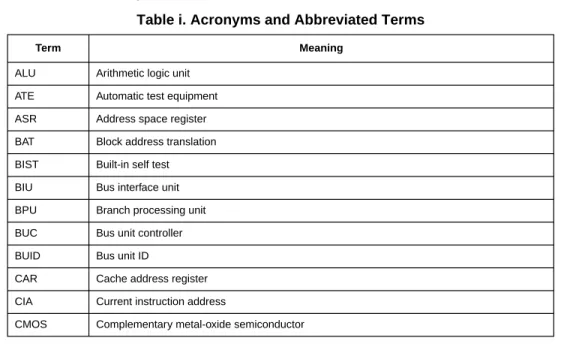
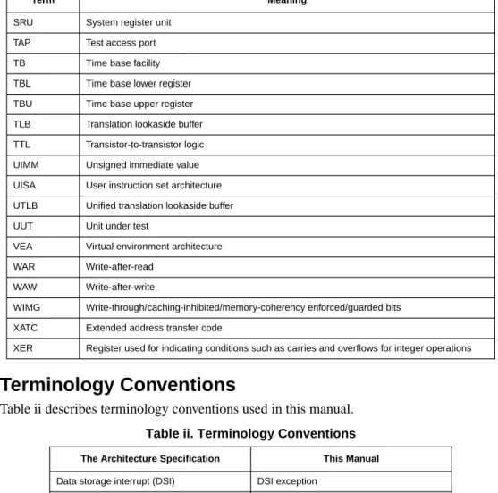
Acronyms and Abbreviations
Table i contains acronyms and abbreviations that are used in this document.
Table i. Acronyms and Abbreviated Terms
Term Meaning
ALU Arithmetic logic unit ATE Automatic test equipment ASR Address space register BAT Block address translation BIST Built-in self test BIU Bus interface unit BPU Branch processing unit BUC Bus unit controller BUID Bus unit ID
CAR Cache address register CIA Current instruction address
CMOS Complementary metal-oxide semiconductor
COP Common on-chip processor CR Condition register CRTRY Cache retry queue CTR Count register DAR Data address register DBAT Data BAT
DCMP Data TLB compare DEC Decrementer register DMISS Data TLB miss address
DSISR Register used for determining the source of a DSI exception DTLB Data translation lookaside buffer
EA Effective address EAR External access register ECC Error checking and correction FIFO First-in-first-out
FPR Floating-point register
FPSCR Floating-point status and control register FPU Floating-point unit
GPR General-purpose register HASH1 Primary hash address HASH2 Secondary hash address
IABR Instruction address breakpoint register IBAT Instruction BAT
ICMP Instruction TLB compare
IEEE Institute for Electrical and Electronics Engineers IMISS Instruction TLB miss address
IQ Instruction queue
ITLB Instruction translation lookaside buffer IU Integer unit
L2 Secondary cache LIFO Last-in-first-out LR Link register
Table i. Acronyms and Abbreviated Terms (Continued)
LRU Least recently used LSB Least-significant byte lsb Least-significant bit LSU Load/store unit MEI Modified/exclusive/invalid
MESI Modified/exclusive/shared/invalid—cache coherency protocol MMU Memory management unit
MQ MQ register MSB Most-significant byte msb Most-significant bit MSR Machine state register NaN Not a number No-op No operation
OEA Operating environment architecture PID Processor identification tag PIR Processor identification register PLL Phase-locked loop
POWER Performance Optimized with Enhanced RISC architecture PTE Page table entry
PTEG Page table entry group PVR Processor version register RAW Read-after-write
RISC Reduced instruction set computing RPA Required physical address RTL Register transfer language RWITM Read with intent to modify
SDR1 Register that specifies the page table base address for virtual-to-physical address translation SLB Segment lookaside buffer
SPR Special-purpose register SR Segment register
SRR0 Machine status save/restore register 0 SRR1 Machine status save/restore register 1
Table i. Acronyms and Abbreviated Terms (Continued)
Terminology Conventions
Table ii describes terminology conventions used in this manual.
SRU System register unit TAP Test access port TB Time base facility TBL Time base lower register TBU Time base upper register TLB Translation lookaside buffer TTL Transistor-to-transistor logic UIMM Unsigned immediate value UISA User instruction set architecture UTLB Unified translation lookaside buffer UUT Unit under test
VEA Virtual environment architecture WAR Write-after-read
WAW Write-after-write
WIMG Write-through/caching-inhibited/memory-coherency enforced/guarded bits XATC Extended address transfer code
XER Register used for indicating conditions such as carries and overflows for integer operations
Table ii. Terminology Conventions
The Architecture Specification This Manual
Data storage interrupt (DSI) DSI exception Extended mnemonics Simplified mnemonics Fixed-point unit (FXU) Integer unit (IU) Instruction storage interrupt (ISI) ISI exception Interrupt Exception
Privileged mode (or privileged state) Supervisor-level privilege Problem mode (or problem state) User-level privilege Real address Physical address Relocation Translation Storage (locations) Memory
Table i. Acronyms and Abbreviated Terms (Continued)
Table iii describes instruction field notation used in this manual.
Storage (the act of) Access Store in Write back Store through Write through
Table iii. Instruction Field Conventions
The Architecture Specification Equivalent to:
BA, BB, BT crbA, crbB, crbD (respectively)
BF, BFA crfD, crfS (respectively)
D d
DS ds
FLM FM
FRA, FRB, FRC, FRT, FRS frA, frB, frC, frD, frS (respectively)
FXM CRM
RA, RB, RT, RS rA, rB, rD, rS (respectively)
SI SIMM
U IMM
UI UIMM
/, //, /// 0...0 (shaded)
Table ii. Terminology Conventions (Continued)
Chapter 1
Overview
1010
This chapter provides an overview of the PowerPC 604e™ microprocessor. It includes the following:
• A summary of 604e features
• Details about the 604e as an implementation of the PowerPC™ architecure. This includes descriptions of the 604e’s execution model (that is, the programming model).
• A description of the 604e execution model. This section includes information about the programming model, instruction set, exception model, and instruction timing.
1.1 Overview
The 604e is an implementation of the PowerPC family of reduced instruction set computer (RISC) microprocessors. The 604e implements the PowerPC architecture as it is specified for 32-bit addressing, which provides 32-bit effective (logical) addresses, integer data types of 8, 16, and 32 bits, and floating-point data types of 32 and 64 bits (single- and double-precision, respectively). For 64-bit PowerPC implementations, the PowerPC architecture provides additional 64-bit integer data types, 64-bit addressing, and related features.
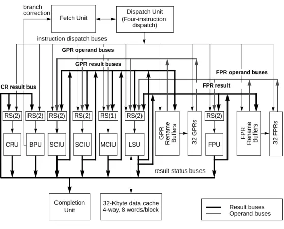
The 604e is a superscalar processor capable of issuing four instructions simultaneously. As many as seven instructions can finish execution in parallel. The 604e has seven execution units that can operate in parallel:
• Floating-point unit (FPU) • Branch processing unit (BPU) • Condition register unit (CRU) • Load/store unit (LSU)
• Three integer units (IUs):
— Two single-cycle integer units (SCIUs) — One multiple-cycle integer unit (MCIU)
The 604e’s rename buffers, reservation stations, dynamic branch prediction, and completion unit increase instruction throughput, guarantee in-order completion, and ensure a precise exception model. (Note that the PowerPC architecture specification refers to all exceptions as interrupts.)
The 604e has separate memory management units (MMUs) and separate 32-Kbyte on-chip caches for instructions and data. The 604e implements two 128-entry, two-way set associative translation lookaside buffers (TLBs), one for instructions and one for data, and provides support for demand-paged virtual memory address translation and variable-sized block translation. The TLBs and the cache use least-recently used (LRU) replacement algorithms.
The 604e has a 64-bit external data bus and a 32-bit address bus. The 604e interface protocol allows multiple masters to compete for system resources through a central external arbiter. Additionally, on-chip snooping logic maintains data cache coherency for multiprocessor applications. The 604e supports single-beat and burst data transfers for memory accesses and memory-mapped I/O accesses.
The 604e uses an advanced, 2.5-V CMOS process technology and is fully compatible with TTL devices.
1.2 PowerPC 604e Microprocessor Features
This section describes features of the 604e, provides a block diagram showing the major functional units, and describes briefly how those units interact.
Figure 1-1 provides a block diagram showing features of the 604e. Note that this is a conceptual diagram that shows basic features and does not attempt to show how these features are physically implemented on the chip.
Branch Processing Unit
72-BIT DATA BUS
36-BIT ADDRESS BUS
Instruction
Queue (8 word)
INSTRUCTION UNIT
Floating- Point Unit
+ * / FPSCR BUS INTERFACE UNIT 64 Bit 32 Bit 128 Bit COMPLETION UNIT 16-Entry Reorder Buffer Time-Base Counter/Decrementer Clock Multiplier JTAG/COP Interface 128 Bit 64 Bit 64 Bit 128 Bit Dispatch Unit + / Cycle Integer Unit I MMU SRs ITLB IBAT Array CR Rename- Buffers (8) CTR CR LR BTAC BHT * / Single-Cycle Integer Units + 32 Bit 32 Bit 32 Bit 32 Bit 16-Kbyte I Cache Tags 16-Kbyte D Cache Tags GPR File Rename Buffers (12)
FPR File Rename Buffers (8)
64 Bit 64 Bit D MMU SRs DTLB DBAT array Reservation Station (2 Entry) Reservation Station (2 Entry) Reservation Station (2 Entry) Reservation Station (2 Entry) Finish Load Queue Store Queue Snoop Fetcher Load/Store Unit EA Calculation +
Major features of the 604e are as follows:
• High-performance, superscalar microprocessor
— As many as four instructions can be issued per clock
— As many as seven instructions can be executing per clock (including three integer instructions)
— Single-clock-cycle execution for most instructions • Seven independent execution units and two register files
— BPU featuring dynamic branch prediction – Two-entry reservation station
– Out-of-order execution through two branches – Shares dispatch bus with CRU
– 64-entry fully-associative branch target address cache (BTAC). In the 604e, the BTAC can be disabled and invalidated.
– 512-entry branch history table (BHT) with two bits per entry for four levels of prediction—not-taken, strongly not-taken, taken, strongly taken
— Condition register unit (CRU) – Two-entry reservation station – Shares dispatch bus with BPU
— Two single-cycle IUs (SCIUs) and one multiple-cycle IU (MCIU) – Instructions that execute in the SCIU take one cycle to execute; most
instructions that execute in the MCIU take multiple cycles to execute. – Each SCIU has a two-entry reservation station to minimize stalls
– The MCIU has a single-entry reservation station and provides early exit (three cycles) for 16- x 32-bit and overflow operations.
– Thirty-two GPRs for integer operands — Three-stage floating-point unit (FPU)
– Fully IEEE 754-1985-compliant FPU for both single- and double-precision operations
– Supports non-IEEE mode for time-critical operations – Fully pipelined, single-pass double-precision design – Hardware support for denormalized numbers – Two-entry reservation station to minimize stalls
– Thirty-two 64-bit FPRs for single- or double-precision operands — Load/store unit (LSU)
– Two-entry reservation station to minimize stalls – Single-cycle, pipelined cache access
– Performs alignment and precision conversion for floating-point data – Performs alignment and sign extension for integer data
– Four-entry finish load queue (FLQ) provides load miss buffering – Six-entry store queue
– Supports both big- and little-endian modes • Rename buffers
— Twelve GPR rename buffers — Eight FPR rename buffers
— Eight condition register (CR) rename buffers • Completion unit
— Retires an instruction from the 16-entry reorder buffer when all instructions ahead of it have been completed and the instruction has finished execution. — Guarantees sequential programming model (precise exception model) — Monitors all dispatched instructions and retires them in order
— Tracks unresolved branches and flushes executed, dispatched, and fetched instructions if branch is mispredicted
— Retires as many as four instructions per clock
• Separate on-chip instruction and data caches (Harvard architecture) — 32-Kbyte, four-way set-associative instruction and data caches — LRU replacement algorithm
— 32-byte (eight-word) cache block size
— Physically indexed/physical tags. (Note that the PowerPC architecture refers to physical address space as real address space.)
— Cache write-back or write-through operation programmable on a per page or per block basis
— Instruction cache can provide four instructions per clock; data cache can provide two words per clock.
— Caches can be disabled in software. — Caches can be locked.
— Parity checking performed on both caches
— Data cache coherency (MESI) maintained in hardware — Secondary data cache support provided
— Instruction cache coherency optionally maintained in hardware
— Data cache line-fill buffer forwarding. In the 604, only the critical double word of the cache block was made available to the requesting unit at the time it was burst into the line-fill buffer; subsequent data was unavailable until the cache block was filled. In the 604e, subsequent data is also made available as it arrives in the line-fill buffer.
• Separate memory management units (MMUs) for instructions and data
— Address translation facilities for 4-Kbyte page size, variable block size, and 256-Mbyte segment size
— Both TLBs are 128-entry and two-way set associative — The page table search is performed in hardware
— Separate IBATs and DBATs (four each) also defined as SPRs — Separate instruction and data translation lookaside buffers (TLBs) — LRU replacement algorithm
— 52-bit virtual address; 32-bit physical address • Bus interface features include the following:
— Selectable processor-to-bus clock frequency ratios (1:1, 3:2, 2:1, 5:2, 3:1, 7:2, and 4:1)
— A 64-bit split-transaction external data bus with burst transfers
— Support for address pipelining and limited out-of-order bus transactions — Four burst write queues—three for cache copy-back operations and one for
snoop push operations — Two single-beat write queues
— Additional signals and signal redefinition for direct-store operations
— Provides a data streaming mode that allows consecutive burst read data transfers to occur without intervening dead cycles. This mode also disables data retry operations.
— No-DRTRY mode eliminates the DRTRY signal from the qualified data bus grant condition. This improves performance on read operations for systems that do not use the DRTRY signal. No-DRTRY mode makes read data available to the processor one bus clock cycle sooner than if normal mode is used.
• Multiprocessing support features include the following:
— Hardware enforced, four-state cache coherency protocol (MESI) for data cache. Bits are provided in the instruction cache to indicate only whether a cache block is valid or invalid.
— Separate port into data cache tags for bus snooping
— Load/store with reservation instruction pair for atomic memory references, semaphores, and other multiprocessor operations
• Power management
— Nap mode supports full shut down and snooping
— Operating voltage of 2.5 ± 0.2 V for processor core, 3.3 V for external signals • Performance monitor can be used to help in debugging system designs and
improving software efficiency, especially in multiprocessor systems. • In-system testability and debugging features through JTAG boundary-scan
Features of the 604e that are not implemented in the 604 are as follows: • Additional special-purpose registers
— Hardware implementation-dependent register 1 (HID1) provides four read-only PLL_CFG bits for indicating the processor/bus clock ratio.
— Three additional registers to support the performance monitor—MMCR1 is a second control register that includes bits to support the use of two additional counter registers, PMC3 and PMC4.
• Instruction execution
— Separate execution units for branch and condition register (CR) instructions. The 604e implements a condition register unit (CRU) that executes condition register logical instructions that were executed in the 604’s BPU. The CRU makes it possible for branch instructions to execute and resolve before preceding CR logical instructions. The 604e can dispatch one CR logical or branch instruction per cycle, but it can execute both branch and CR logical instructions at the same time.
— Branch correction in decode stage. Branch correction in the decode stage can now predict branches whose target is taken from the count or link registers if no updates of the count and link register are pending. This saves at least one cycle on branch correction when the Move to Special-Purpose Register (mtspr) instruction can be sufficiently separated from the branch that uses the SPR as a target address.
— Ability to disable the branch target address cache (BTAC)—HID0[30] has been defined to allow the BTAC to be disabled. When HID0[30] is set, the BTAC contents are invalidated and the BTAC behaves as if it were empty. New entries cannot be added until the BTAC is enabled.
• Enhancements to cache implementation
— 32-Kbyte, physically addressed, split data and instruction caches. Like the 604, both caches are four-way set associative; however, each cache has twice as many sets, logically separated into 128 sets of odd lines and 128 sets of even lines. — Data cache line-fill buffer forwarding. In the 604, only the critical double word
of a burst operation was made available to the requesting unit at the time it was burst into the line-fill buffer. Subsequent data was unavailable until the cache block was filled. In the 604e, subsequent data is also made available as it arrives in the line-fill buffer.
— Additional cache copy-back buffers. The 604e implements three copy-back write buffers (increased from one in the 604). Having multiple copy-back buffers provides the ability for certain instructions to take fuller advantage of the pipelined system bus to provide more efficient handling of cache copy-back, block invalidate operations caused by the Data Cache Block Flush (dcbf) instruction, and cache block clean operations resulting from the Data Cache Block Store (dcbst) instruction.