Optimisation of Switching Losses and Capacitor
Voltage Ripple Using Model Predictive Control of a
Cascaded H-bridge Multi-level StatCom
Mr Christopher D. Townsend
1, Dr Terrence J. Summers
2,
Dr John Vodden
3, Dr Alan J. Watson
4, Professor Robert E. Betz,
5Professor Jon C. Clare
61,2,5
School of Electrical Engineering and Computer Science
University of Newcastle, Australia, 2308
3,4,6School of Electrical and Electronic Engineering
University of Nottingham, United Kingdom
email:
1[email protected]
2
[email protected]
3
[email protected]
4
[email protected]
5
[email protected]
6
[email protected]
Abstract—This paper further develops a Model Predictive Control (MPC) scheme which is able to exploit the large number of redundant switching states available in a multi-level H-bridge StatCom (H-StatCom). The new sections of the scheme provide optimised methods to trade off the harmonic performance with converter switching losses and capacitor voltage ripple. Varying the pulse placement within the modulation scheme and modifying the heuristic model of the voltage balancing characteristics allows the MPC scheme to achieve superior performance to that of the industry standard phase shifted carrier modulation technique. The effects of capacitor voltage ripple on the lifetime of the capacitors is also investigated. It is shown that the MPC scheme can reduce capacitor voltage ripple and increase capacitor lifetime. Simulation and experimental results are presented that confirm the correct operation of the control and modulation strategies.
Index Terms – Multi-level converters, StatCom, voltage bal-ancing, modulation strategy, control strategy
I. INTRODUCTION
The Cascaded H-bridge converter is becoming a popu-lar topology for multi-level Static Compensators (StatComs). There are a number of reasons for this, but the main one is that it is feasible to obtain a large number of levels with this topology [1], [2]. With alternative topologies the level numbers are constrained by component number and capacitor voltage balance issues [3]. The increased number of levels achievable with the H-bridge multi-level converter also allows greater switching redundancy, which creates more flexibility in terms of the ability to trade-off between harmonic performance, switching losses and voltage balancing.
The modulation techniques most commonly used to syn-thesise the required voltage at the output of a H-StatCom have been adapted from typical multi-level applications such as electric drives [4]. These techniques include Selective
Harmonic Elimination (SHE) which uses precomputed firing angles to modulate the H-bridges [5], [6], and Phase-Shifted Carrier (PSC) PWM that uses comparisons with multiple trian-gular carrier waves to derive the appropriate switching signals [7], [8]. The complexity involved in solving the transcendental equations in SHE-PWM for a wide range of input conditions has limited the use of the technique. While the main drawback of PSC-PWM is the control interactions that occur between the multiple required voltage balancing loops [9], [10].
The control and modulation techniques described in this paper utilise instantaneous power theory [11], [12] coupled with dead-beat current control, heuristic models of voltage balancing and switching loss, and traditional PWM. One of the main advantages of utilising this technique is the ability to balance the H-bridge capacitor voltages by choosing which capacitors are used to create the output voltage. This inherently allows the leg cluster voltage (defined as the sum of the capacitor voltages within a particular phase-leg) to be shared evenly across the individual H-bridge capacitors. The cluster voltage is regulated at a set-point value through a separate control loop [13]. This technique avoids the control loop interaction problems present in PSC-PWM strategies.
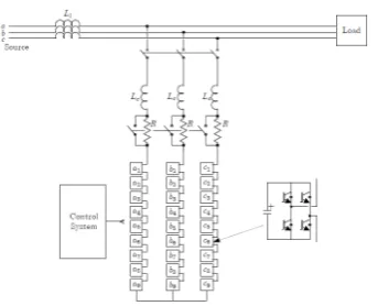
Figure 1. Circuit configuration of a star-connected 19-level H-bridge StatCom.
indicators. Variation of the pulse placement within the PWM scheme is also investigated. When coupled with the MPC cost function, variation of pulse placement can significantly reduce the switching transitions and hence switching losses. Finally, we compare the performance of the proposed MPC scheme with that of a Space Vector Modulation (SVM) scheme proposed for use in H-StatComs [15]. It is shown that while the SVM scheme achieves an excellent trade-off between the switching frequency and harmonic performance there are also important effects on the capacitor lifetime that are a result of the ripple currents created.
II. BACKGROUND
Fig. 1 shows the circuit configuration for a 19-level (line to neutral) H-StatCom. Fig. 2 is a block diagram of the scheme used to control the H-StatCom. The details of the outer control loops that are responsible for generating the current references have been presented in [14] and will not be repeated here. The desired output voltages, which are calculated by the dead-beat controller, are used directly within the ‘MPC’ block. Therefore, details of the current controller will be provided to clarify the operation of the MPC scheme.
The dead-beat control equations used to calculate the re-quired output H-StatCom voltage are shown in (1) and (2).
vrefk+1= L
T(i ref
k+1−ˆik) + ˆvkref+0.5 (1)
ˆik=ik−1+T
L(vk−v sys
k−0.5) (2) Where ik−1 is the instantaneous sample of the current at time t = (k−1)T and iref
k+1 is the instantaneous value of the reference current at timet= (k+ 1)T. As for the voltage nomenclature,vk is the actual voltage applied during the
inter-val from(k−1)T →kT ,vkref+1 is the desired (or reference) voltage that the controller applies from kT → (k+ 1)T,
ˆ
vref
k+0.5 is the predicted instantaneous supply voltage at the midpoint of the control interval from kT → (k+ 1)T and vksys−0.5 is the measured instantaneous supply voltage at the midpoint of the control interval from (k−1)T →kT. T is the control period andLis the connection inductance between the H-StatCom and the three-phase system.
PWM Gen MPC
vg Vector
Voltage Limiter Deadbeat
Current Control
vr Vector
Current Limiter
ir vrlim
Leg Voltage Control vg
vla; vlb; vlc
iP r
vrleg
isc isc
isc
S = iscv¤g
vrlim
Power Measurement Qr
+
-§ iQ
r=vS¤g
Pr= 0
iQ
r vector
Power System
vg Power Control
vg
vg isc Qsc
Psc
Vdc1::27
Vres
sw1;2;3 PQ
KPs+KI
s
vla; vlb; vlc
vg
Figure 2. Block diagram of the H-StatCom control with MPC.
The authors have implemented three cost functions to reduce computation time. Each cost function evaluates the possible switching combinations for one phase-leg within the three-phase system. Initially the desired output voltages for each phase are calculated in the dead-beat current controller. The ‘MPC’ block then evaluates the corresponding voltage vector for each switching combination using (3).
vkapp+1=Vdc•Si (3)
wherek∈I,vkapp+1 is the applied voltage vector generated by the switching statesSi, for the interval fromkT →(k+ 1)T.
By comparing to the desired output voltages calculated in the dead-beat controller, combinations that produce a residual voltage greater than the lowest capacitor voltage are dis-regarded. This evaluation is performed by disregarding any combinations that do not satisfy the condition in (4).
vrefk+1−v
app
k+1
< Vdc,min (4) whereVdc,minis the minimum capacitor voltage within the phase-leg andvrefk+1 is the reference voltage (calculated within the dead-beat controller) that the scheme needs to apply from kT →(k+ 1)T.
The remaining switching combinations are evaluated in an MPC cost function that includes heuristic models of the voltage balancing and switching loss characteristics. The form of the cost function is:
error=α1(Vcap,error) +α2(SWtransitions) (5) where SWtransitions is the number of transitions from the currently applied switching combination to the evaluated com-bination and Vcap,error is a measure of how far the evaluated combination will drive the capacitor voltages either towards or further from their target value.
[image:2.595.315.545.52.204.2]appropriate bridge. The most appropriate bridge is determined by first sorting the capacitor voltages then selecting the H-bridge with the lowest voltage (or highest voltage depending on the direction of instantaneous power flow) that has not already been switched in by the MPC scheme. The application of the residual voltage provides excellent current tracking performance and reduces the Total Harmonic Distortion (THD) of the H-StatCom current.
III. CAPACITORVOLTAGEBALANCING
The ‘MPC’ and ‘PWM Gen’ blocks have been modified to investigate the trade-off between harmonic performance and switching losses. Previously the ‘MPC’ block integrated the deadbeat control equations with a logic based penalisation of the voltage balancing [14]. This type of penalisation is simple to implement and has a relatively small execution time due its exclusive use of bitwise evaluations. However, because the capacitor voltages are only evaluated with respect to each other (via a sorting operation), there is no way to penalise larger errors between the target and measured voltages.
Here a new model is proposed for the voltage balancing of the capacitors. The new model is applied using the following steps to calculate theVcap,error term in (5):
1) Sort the difference between each capacitor voltage and the average of the capacitor voltages, from largest dif-ference to smallest difdif-ference. The result will be an array of N integers with the first element containing the number of the capacitor with the largest positive voltage difference, and the last element containing the number of the capacitor with the largest negative voltage difference. For example consider the sorted array below. In a four bridge phase-leg if capacitor number four has the largest voltage difference then the first element of the array is 1000. In this example if capacitor number three is the furthest below its reference value then the fourth element of the array is 0100;
Cap with largest +ve diff 4 (10.0V)
1 (2.2V) 2 (-5.2V) 3 (-7.0V)
→
Array of Integers 1000 0001 0010 0100
2) If the instantaneous power is flowing into the phase-leg then reverse the order of the differences;
3) Create an N bit number for each possible switching combination. Continuing the example, if capacitors one and four are switched in for a particular combination, while the others are switched out then the corresponding representation is 1001. Examples of how some of the possible switching combinations are represented are shown below;
Caps Switched In 1,4 2,3 1,2,3,4
→
Array of Integers 1001 0110 1111
4) Upon evaluation of each switching combination, bitwise AND each N bit number created in step 3, with each element of the array created in step 1. If the result is non-zero then accumulate an error value which is modulated based on the need for the evaluated capacitor to be switched in. The accumulated error is penalised proportionally to the difference between that capacitor’s reference and measured value. The accumulated error is also modulated with reference to the largest positive voltage difference when power is flowing out of the phase-leg, and measured with reference to the largest negative voltage difference if power is flowing into the leg. Two example switching combinations are shown below. Consider the switching combination where capac-itors one and four are switched in while power is flowing out of the phase-leg. This means capacitors number one and four require discharging while the others require charging. Under this condition the accumulated error will be 2∗(10.0−2.2) + 1∗(10.0−10.0) = 15.6. For the second example switching combination in which capacitors number two and three are switched in the accumulated error would be4∗(10.0−(−7.0)) + 3∗
(10.0−(−5.2)) = 113.6;
Switch Comb Cap Number Error
1001 0100 0
1001 0010 0
1001 0001 2*(10.0-2.2) 1001 1000 1*(10.0-10.0)
Vcap,error 15.6 Switch Comb Cap Number Error
0110 0100 4*(10.0-(-7.0)) 0110 0010 3*(10.0-(-5.2))
0110 0001 0
0110 1000 0
Vcap,error 113.6
Switch Comb Cap Number Error 1001 1000 4*-1*(-7.0-10.0) 1001 0001 3*-1*(-7.0-2.2)
1001 0010 0
1001 0100 0
Vcap,error 95.6 Switch Comb Cap Number Error
0110 1000 0
0110 0001 0
0110 0010 2*-1*(-7.0-(-5.2)) 0110 0100 1*-1*(-7.0-(-7.0))
Vcap,error 3.6
From the example switching combinations that have been considered above it is clear that the new model of the voltage balancing allows increased penalisation of larger errors in the capacitor voltage. The model essentially includes more infor-mation about the system that is being controlled. Therefore, it is much more likely that this model is able to apply a more optimal solution than the bitwise penalisation model.
Remark 1: The use of the new model also reduces capacitor
voltage ripple which can increase capacitor lifetime. The physical mechanisms that quantify the effect on capacitor lifetime are discussed in Section VIII. n The new model also improves the stability of the voltage balancing characteristics due to its ability to distinguish be-tween the case where a capacitor has the lowest voltage but remains close to the reference (and therefore does not need to be switched) and the case where the capacitor has the lowest voltage and has a relatively large difference between its reference and measured value (and therefore should be switched). The logic based penalisation was incapable of distinguishing this difference. It therefore could not optimise the trade-off within the cost function nor enforce the maximum control action to balance the capacitor voltages in situations where there was a high degree of unbalance.
The new model can also regulate capacitor voltages at different target values. This makes the MPC scheme appli-cable to asymmetric modulation schemes that can be used to improve the harmonic performance of the H-StatCom system for particular applications [16]. The new model is also well suited to the implementation of large scale PhotoVoltaic (PV) systems. It has the ability to inherently balance the DC link voltages while also modifying any of those voltages. Such independent control over the DC links allows tracking of the maximum power points associated with multiple PV arrays [17], [18].
IV. VARIATION OFPULSEPLACEMENT
It was shown in [14] that the inclusion of a MPC cost function can be used to reduce the average switching frequency by keeping the H-bridges switched in for longer periods. It was noted in [14] that the main limitation in further reducing the switching losses was the number of transitions that result from one of the H-bridges in the phase-leg being symmetrically pulse width modulated.
In [14] the voltage pulse was placed in the centre of the control period to improve harmonic performance [19]. However the number of switching transitions can be signif-icantly reduced by moving the pulse to the beginning of the control period. Given this observation, in each control cycle the following procedure is undertaken within the ‘PWM Gen’ block, shown in Fig. 2, to determine if the switching transitions can be reduced for the subsequent interval.
1) The switching combination for the next interval, that has been determined in the ‘MPC’ block, is passed in along with the residual volt seconds. The residual volt seconds are calculated as part of the MPC algorithm and correspond to the difference between the voltage determined by the dead-beat controller and the voltage chosen by the MPC controller;
2) If the total voltage to be applied at the output of the stack is positive, and the residual volt seconds is positive, then the switching combination that is currently being applied is compared to the chosen combination for the next control interval. Each H-bridge is evaluated to determine if any are currently switched in, but due to be switched out for the next interval. Under this condition the H-bridge can be left in at the beginning of the next interval and then switched out after an appropriate time that depends on the magnitude of the residual volt seconds which needs to be created;
3) If the total voltage to be applied at the output of the stack is negative and the residual volt seconds is negative, then the two switching combinations (present and future) are evaluated for the same condition as in step 2 i.e. a H-bridge that is currently switched in but due to be switched out. As in step 2, the H-bridge is left switched in for an appropriate time to create the residual volt seconds and then switched out;
4) If the total voltage to be applied at the output of the stack is positive, and the residual volt seconds is negative, then the two switching combinations are evaluated to deter-mine if there are any H-bridges switched in currently that will remain switched in during the next interval. Under this condition the H-bridge can be switched out early to reduce the total volt seconds. In this case, a signal is sent back to the ‘MPC’ block to tell the algorithm that this H-bridge has been switched out. This allows the MPC cost function to attempt to keep this bridge in a constant state and hence reduce the total switching transitions;
[image:4.595.64.282.52.206.2]5) If the total voltage to be applied at the output of the stack is negative, and the residual volt seconds is positive, then the two switching combinations are evaluated for the same condition as in step 4 i.e. a H-bridge that is currently switched in that is to remain switched in. As in step 4, the H-bridge is switched out after an appropriate time to account for the residual volt seconds, while the MPC block is informed that this H-bridge has been switched out.
ton ton
T T
T =2 T =2 ton
ton
(a) (a)
(b) (b)
nVdc
nVdc
(n+ 1)Vdc
(n+ 1)Vdc
nVdc nVdc
(n+ 1)Vdc
[image:5.595.46.291.50.172.2](n+ 1)Vdc
Figure 3. Top section of the H-StatCom output voltage waveforms for (a) Symmetrical PWM (b) Pulse variation method.
allows for an overall reduction in switching transitions. Note that Fig. 3 depicts a zoomed in look at the top of two H-StatCom output voltage waveforms wherenis an integer that varies depending on which part of the output voltage waveform is being synthesised.
Along with the reduction in switching transitions it is also evident from Fig. 3 that the harmonic performance must suffer some degradation as a result of the pulse no longer being centered. This trade-off is quantified in Sections V and VI.
V. SIMULATION RESULTS
A comprehensive simulation of the MPC scheme developed in this paper has been implemented in Saberr. The sampling time in the simulated system is400µs.
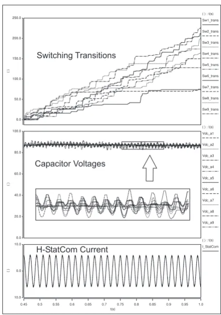
Fig. 4 confirms the correct operation of the proposed voltage balancing scheme and the pulse variation strategy. These simulation results depict the condition where the H-StatCom is absorbing2.0kvar capacitive. The excellent current tracking performance is shown along with the nine phase ‘a’ capacitor voltages which are successfully sharing the leg cluster voltage. The capacitor voltages all have the normal100Hz ripple com-ponent present in H-StatCom systems, however the deviation of the capacitor voltages from the mean DC value has been decreased by approximately30% when compared to the use of the previous balancing scheme [14].
The number of switching transitions that occur on leg ‘a’ of the nine phase ‘a’ H-bridges is also shown in Fig. 4. The average number of transitions that occurs on each switch for the0.55s period is 158.
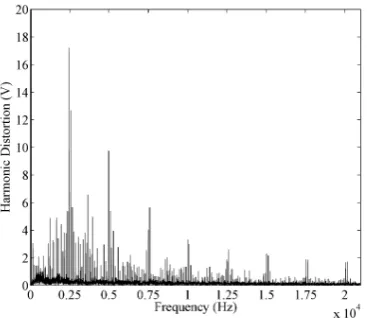
Fig.5 shows a close-up of the H-StatCom current and output voltage when the H-StatCom is absorbing2.0kvar inductive. Fourier analysis on the output voltage has been performed and the spectrum is also shown in Fig.5. As expected the pulse placement technique spreads the resultant spectrum and induces significant harmonics into the region below the original switching frequency (2.5kHz). This will result in an increase in THD. By performing a FFT on the H-StatCom current signal the THD is calculated at3.1%.
[image:5.595.314.542.67.392.2]The authors have developed a H-StatCom simulation which calculates the performance of a particular PSC-PWM scheme [10]. This simulation provides the theoretical values of total harmonic distortion which can be achieved within the H-StatCom system.
Figure 4. Simulation waveforms for phase ‘a’ for the new pulse placement scheme with scaling factorsα1= 0.02andα2= 0.4- Top plot: switching
transitions, Middle plot: nine bridge capacitor voltages, Bottom plot: H-StatCom measured current.
Current (A)
−5.0 0.0 5.0
t(s)
0.605 0.61 0.615 0.62 0.625 0.63 0.635 0.64 0.645 f(Hz)
0.0 2.0k 4.0k 6.0k 8.0k 10.0k 12.0k 14.0k
Voltage (V)
−500.0 0.0 500.0
Mag(V)
0.0 10.0 20.0 30.0 40.0
Current (A) : t(s)
I_StatCom
Voltage (V) : t(s)
V_StatCom
Mag(V) : f(Hz)
V_StatCom
Figure 5. Simulation waveforms for phase ‘a’ for the new pulse placement scheme with scaling factorsα1= 0.02andα2= 0.4- Top plot: Spectra of
[image:5.595.315.544.479.659.2]To gain similar harmonic performance to that of the MPC scheme described in this paper, the PSC-PWM simulation requires a carrier frequency of 194Hz. For PSC-PWM each switching device will undergo two switching transitions per period of the carrier waveform, this is due to the fact that PSC-PWM switches in each bridge during every period of the carrier waveform. This means the total switching transitions per component for a 0.55s period of time will be 213. Therefore, the simulation results show that the MPC algorithm is capable of exceeding the performance of PSC-PWM by up to35%.
In Fig.4 it is clear that during the simulation interval the switching transitions are not distributed evenly between the bridge modules. This scenario is not acceptable within H-StatCom systems because all the H-bridge modules would need to be designed to satisfy the most restrictive case i.e. to guarantee the cooling requirements are satisfied the modules would need to be sized based on the maximum number of switching transitions that are occurring, not the average number of transitions throughout the phase-leg.
There are two solutions to address any uneven distribution. The first is to incorporate extra models within the MPC cost function which penalise not only the total number of switching transitions but also where in the phase-leg those transitions are occurring. This however would increase the complexity of the cost function and more importantly increase the already significant execution time. The second option is to take advantage of an extra degree of freedom which the proposed MPC scheme provides. After the MPC cost function has chosen which capacitors are to be used to create the output voltage there still remains a decision to be made within the modulation structure. This decision is, which of the capacitors will be used to create the residual voltage. It is simple to modify the modulation structure so that the modules which have experienced the least number of transitions in a past interval are chosen to create the residual voltage. This has the effect of smoothing out the number of transitions without significantly affecting the computational power required to implement the scheme.
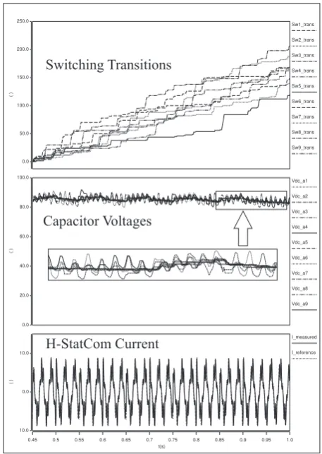
Fig. 6 shows waveforms for the situation where the H-StatCom is both supplying significant amounts of harmonic correction and undergoing frequent transient changes from absorbing inductive to absorbing capacitive Vars. The average number of transitions that occur on each switch for the0.55s period is162. This is only 4 more average transitions than the steady state case. This demonstrates that even when the H-StatCom is compensating for highly dynamic and distorted networks the trade-off between harmonic performance and switching losses for the MPC scheme will not be greatly affected.
VI. EXPERIMENTALRESULTS
[image:6.595.314.543.52.374.2]A low voltage (415VAC) 19-level H-bridge StatCom has been utilised to validate the simulation studies and further investigate the performance of the proposed MPC and pulse variation techniques. The H-StatCom used to produce the
Figure 6. Simulation waveforms for phase ‘a’ for a highly dynamic operational condition with scaling factors α1 = 0.02 and α2 = 0.4
-Top plot: switching transitions, Middle plot: nine H-bridge capacitor voltages, Bottom plot: H-StatCom measured current.
experimental results has 9 H-bridges per phase, with each H-bridge designed with MOSFET power devices. The phase legs are Wye connected. A block diagram of the experimental system appears in Fig. 7. One can see that it is implemented as a multi-processor system, with individual processors imple-menting the control for each of the phase legs. These phase leg processors are responsible for switching in the desired capacitors and applying the PWM. The desired switching combinations which are passed to the phase leg controllers are developed in the MPC algorithm, which is implemented in a central Pentium IV PC. The sampling time in the experimental setup is 400µs. To execute the control scheme described in this paper the Pentium IV processor requires approximately
140µs.
Fig. 8 shows the measured ‘a’ phase H-StatCom current and the reference current (top plot), and the nine capacitor voltages for phase ‘a’ (bottom plot) when the H-StatCom is absorbing 1.3kvar inductive. It can be seen in Fig. 8 that the system achieves a good current tracking performance with tight control over the capacitor voltages. The capacitors are being regulated at different voltage levels to confirm the correct operation of the new voltage balancing scheme.
HB 1
HB 2
HB 3
Source side Load side
Phase Ctrl 1 Phase
Ctrl 2 Phase
Ctrl 3 Dual
Processor Windows XP/
RTX Control Computer
4 clkf DI/O RS422
Serial Digital parallel/serial
to optical interface Control line key
Serial line Digital line Three lines > three lines
Three phase lines
Protection Power circuitry
Serial Cabinet Monitoring
9´Serial lines Sample
[image:7.595.66.267.49.229.2]Analogue to serial
Figure 7. Block diagram of the experimental system.
Figure 8. Experimental H-StatCom waveforms for phase ‘a’ with scaling factors α1 = 0.05 and α2 = 0.3: - Top plot: H-StatCom measured and
reference current, Bottom plot: nine H-bridge capacitor voltages.
for phases ‘a’ and ‘b’ on the top plot. It can be seen that variation of the pulse placement is occurring on phase ‘a’, while phase ‘b’ is modulated using pulse centered PWM for comparison purposes. Fig.s 10 and 11 show the experimental Fourier spectra of the output H-StatCom voltage for the pulse centered PWM scheme and the new pulse placement modulation scheme respectively. As expected the pulse place-ment technique spreads the resultant spectrum and induces significant sub-harmonics into the region below the original switching frequency (2.5kHz). This results in an increase of THD from1.9% in the symmetrical PWM scheme to2.7% in the pulse placement scheme.
[image:7.595.315.540.53.191.2]The number of transitions that occur on leg ‘a’ of the nine phase ‘a’ H-bridges was measured within the individual phase-leg processor. The average number of transitions that occurs on each switch for a20s period is6,630. The average number of transitions measured on each switch within the simulation for an equivalent operational condition was6,467. The equivalent PSC-PWM scheme with a carrier frequency of 194Hz will experience 7,760 transitions. Therefore, for this operational condition the hardware results show that the MPC algorithm is capable of exceeding the performance of the PSC-PWM scheme by20%. This result confirms the simulation models
Figure 9. Experimental H-StatCom waveforms with scaling factorsα1 =
0.05andα2= 0.3: - Top plot: phases ‘a’ and ‘b’ H-StatCom output voltage,
Bottom plot: measured H-StatCom current.
Figure 10. Spectra of H-StatCom output voltage for the original pulse placement scheme.
and the effectiveness of the new balancing scheme coupled with the variation in pulse placement technique.
VII. COSTFUNCTIONSCALINGFACTORS
The simulation and experimental results demonstrate that the pulse variation method can significantly reduce the number of switching transitions. The trade-off between harmonic per-formance, switching loss and voltage balancing characteristics becomes more complex when the pulse variation technique is utilised. When the penalisation of the switching losses within the cost function is zero the pulse variation technique has a large number of opportunities to vary the pulse placement. This will result in a relatively high THD value for this setting. As the penalisation increases the effect on THD of the pulse variation method is decreased as the savings on switching transitions occur increasingly through decisions made in the cost function. In light of this observation it is clear that different scaling factors can be chosen depending on which performance indicators the control system wishes to optimise at any one time.
[image:7.595.334.518.248.409.2] [image:7.595.54.278.261.392.2]Figure 11. Spectra of H-StatCom output voltage for the new pulse placement scheme for scaling factorsα1= 0.05andα2= 0.3.
of the current tracking does not affect the average volt seconds applied within a control interval, provided that the residual voltage error is less than the lowest capacitor voltage. This condition is enforced within the scheme by specifically ex-cluding switching combinations for which this condition is not true. The total applied volt seconds is always precise due to the residual voltage being applied via PWM.
When the performance of the current tracking is guaranteed, the scaling factors can be obtained empirically. When the scaling factor for the voltage balancing model is non-zero and the switching loss scaling factor is set to zero, the voltage balancing will dominate the cost function and give the tightest control over capacitor voltage ripple. A non-zero setting for the switching loss scaling factor reduces device switching. As this value increases the THD will decrease along with the number of switching transitions. However, at some point the product of the THD and number of switching transitions will start to increase due to the fact the pulse variation technique can no longer identify control periods in which switching transitions can be avoided. Just prior to this point is the most optimal setting for the scaling factors if the main control objective is to maximise the effective switching frequency.
VIII. CAPACITORLIFETIME
To provide a more informed choice of cost function scaling factors the effect of the capacitor voltage ripple on capacitor lifetime is considered in this section. A SVM scheme is also described so that the effects on capacitor lifetime from common control and modulation schemes can be compared.
The performance of the MPC scheme will be compared to the SVM scheme proposed in [15]. The schemes will be compared for a 19-level11kV H-StatCom where the value of the H-bridge capacitors have been chosen to minimise the cost and physical size of the design. The switching frequency used to compare the two schemes is1kHz. Such a low switching frequency is often required to meet the cooling requirements of the H-bridge modules in a H-StatCom application.
1
C R
R
R
2
3 1
Dielectric Loss
Capacitance Dielectric Resistance
Electrolyte Resistance
Resistance of Terminals
C2
[image:8.595.359.498.53.158.2]Capacitance
Figure 12. Model of the electrolytic capacitor.
The SVM scheme synthesises the required output voltage by initially transforming the voltage space vector onto a two dimensional plane in which the switching state vectors have only integer components. This allows the three nearest voltage vectors to be easily identified by rounding the two directional components of the desired space vector. Once these vectors are identified the associated duty cycles that are required to synthesise the average output voltage vector can be calculated via simple algebraic equations. The choice of which vectors are used to create the output voltage is also constrained by the need to minimise the resultant number of switching transitions. By integrating this constraint into the modulation scheme the harmonic performance trade-off with the switching losses is greatly improved. This results in the SVM scheme having a superior trade-off over that of the MPC scheme developed in this paper, often by up to 50%. However the performance comes at the cost of an increased voltage ripple on the H-bridge capacitors. The larger voltage ripple occurs due to the limited ability of the SVM scheme to modify the state of a larger number of H-bridge modules, even when there is a high degree of capacitor voltage unbalance in the system. Given this observation this section will attempt to quantify the effect on capacitor lifetime resulting from the form and magnitude of the voltage ripple for the two differing schemes.
The majority of converters utilise electrolytic capacitors to provide ‘stiff’ DC link voltages. A particular model of an electrolytic capacitor is shown in Fig. 12. This relatively complex model is utilised in this paper as it has been shown to more accurately predict heating effects which are of interest in determining capacitor lifetime [20]. ResistanceR3accounts for the relatively small resistance of the foil, tabs and terminals while resistanceR2represents the resistance of the electrolyte. The parallel combination of C1 and R1 account for the complex impedance of the dielectric material and C2 is the nominal capacitance value.
Electrolytic capacitors have a relatively high Equivalent Series Resistance (ESR) which when coupled with ripple current results in real power loss causing an increase in operational temperature. Through degradation mechanisms in-side the capacitor the increase in temperature results in an increasing ESR until such time that the recommended value is exceeded. This signifies that the capacitor is at the end of its lifetime [21].
[image:8.595.72.256.62.221.2]Current (A)-200.0 0.0 200.0
t(s)
0.2 0.21 0.22 0.23 0.24 0.25 0.26 0.27 0.28 0.29
Voltage (V)
0.0 1.0k 2.0k Current (A)-200.0 0.0 200.0
Mag (A)
0.0 50.0 100.0
f(Hz)
0.0 100.0200.0300.0400.0500.0600.0700.0800.0900.0 1.0k 1.1k 1.2k 1.3k 1.4k 1.5k
[image:9.595.52.280.51.194.2]Current (A) : t(s) Ia_meas Voltage (V) : t(s) Vdc_1 Current (A) : t(s) Icap_1 Mag(Icap_1)
Figure 13. Simulation waveforms when utilising the SVM scheme - Top plot: Fourier spectrum of capacitor current, Middle upper plot: Capacitor current, Middle lower plot: Capacitor voltage, Bottom plot: H-StatCom current.
power loss due to ESR is minimised. The ESR of an elec-trolytic capacitor is frequency dependent as shown in (6).
ESR = R1
1 +ω2C2
1R 2 1
+R2be
Tb−Tc
E +R3 (6)
where ω is the frequency, R2b is the base resistance of
the electrolyte measured at temperature Tb, Tc is the core
temperature of the capacitor and E is a constant defining the sensitivity of the resistance to changes in temperature.
From (6) it is obvious that the resistance is highest at low frequencies which means if the current ripple that the capaci-tors are subject to contains higher frequency components, the ESR and hence power loss is less than when the capacitor is subject to currents with lower frequency components.
Fig. 13 shows the resulting form of the capacitor current when utilising the SVM scheme proposed in [15] while the H-StatCom is absorbing 2.0mvar inductive. The associated Fourier spectrum of the capacitor current is also shown. It can be seen that the majority of the ripple current is in the lower end of the spectrum with the largest component at100Hz.
Fig. 14 shows the resulting form of the capacitor current when utilising the extended MPC scheme for the same opera-tional condition. It can be seen that a significant proportion of the ripple current is moved to the higher end of the spectrum with a corresponding decrease at100Hz.
Equation 7 can be evaluated to determine the power loss which the two schemes would dissipate in a typical electrolytic capacitor.
Ploss=
Np
X
n=0
Icap2 ,n·ESR (ωn) (7)
where Np is the largest multiple of the chosen frequency
interval at which to calculate the harmonics, this analysis considers a frequency interval of5Hz up to 2kHz (twice the switching frequency), thereforeNp= 400.
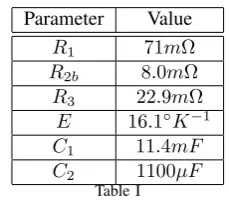
The parameters of the electrolytic capacitor considered in this analysis are shown in Table I. This capacitor was chosen as it is suitable for operation in typical converter applications at the voltage ratings considered in the simulations, based on
Current (A)
−500.0 0.0 500.0
t(s)
0.85 0.86 0.87 0.88 0.89 0.9 0.91 0.92 0.93 0.94 0.95
Voltage (V)
1.0k 1.25k 1.5k 1.75k Current (A) −200.0 0.0 200.0
Mag(A)
0.0 50.0 100.0
f(Hz)
0.0 200.0 400.0 600.0 800.0 1.0k 1.2k 1.4k
Current (A) : t(s)
Ia_meas
[image:9.595.315.544.52.201.2]Voltage (V) : t(s) Vdc_1 Current (A) : t(s) Icap_1 Mag(A) : f(Hz) Icap_1
Figure 14. Simulation waveforms for phase ‘a’ when utilising the MPC scheme with scaling factorsα1 = 0.05and α2 = 0.4- Top plot: Fourier
spectrum of capacitor current, Middle upper plot: Capacitor current, Middle lower plot: Capacitor voltage, Bottom plot: H-StatCom current.
size and cost requirements.
Parameter Value
R1 71mΩ R2b 8.0mΩ
R3 22.9mΩ E 16.1◦K−1 C1 11.4mF C2 1100µF
Table I
ELECTROLYTICCAPACITORPARAMETERS.
Evaluating (7) for the operational conditions depicted in Fig.s 13 and 14 shows that the power loss due to ESR in the MPC scheme is 285W while the SVM scheme causes
560W of real power loss per capacitor. This corresponds to an approximately 200% increase in the ESR power loss when utilising the SVM scheme, compared to when the MPC scheme is employed. This is a direct result of the current ripple having more significant low frequency components in the SVM scheme.
Equation (8) defines the relationship between the power dissipated due to ESR in an electrolytic capacitor and the operating temperature.
4T =PlossRth=Tc−TA (8)
whereTAis the ambient temperature andRthis the thermal
resistance between the case and surrounding air. The thermal resistance is dependent on the surface area of the capacitor and the type of cooling within the installation.
[image:9.595.370.485.294.395.2]Therefore to limit the increase in temperature to50◦C in the MPC scheme we require three capacitors per H-bridge module. The increase in power dissipation with the use of the SVM scheme is 275W, if this is dissipated through three different capacitors it is reasonable to assume a further45◦C increase in the operating temperature of the capacitors. An industry standard rule of thumb for electrolytic capacitors is that increasing the operating temperature by 10◦C halves
the lifetime [23]. Therefore it is obvious that the form of the capacitor voltage ripple seen in the SVM scheme has significant effects on the lifetime of the H-bridge capacitors. In practice this application would require a larger number of capacitors to dissipate the stresses if the SVM scheme is utilised. Obviously this would add significant extra cost to the design of the H-StatCom.
IX. CONTRIBUTIONS& CONCLUSIONS
This paper presents new heuristic models for a MPC scheme which further optimises the trade-off between voltage balanc-ing, switching loss and harmonic performance. These models are integrated with a modified PWM scheme to significantly reduce switching losses. Simulation and experimental results showing the performance of the algorithms in both steady state and transient conditions have been presented. It has been shown that the MPC scheme is capable of out-performing the industry standard phase shifted modulation strategy.
One important limitation of MPC is the computational power required to evaluate the cost function. This paper has developed methods to reduce the required execution times so that the system models can be evaluated for typical control frequencies used in grid connected power electronics. These methods include evaluating the combinations on a per-phase basis, combining traditional modulation concepts of MPC with SV-PWM, and utilising mostly bitwise evaluations to penalise the system models.
As stated, the experimental system described in this paper evaluates the MPC scheme by utilising a powerful Pentium processor. However, due to the simple nature of the heuristic models of the capacitor voltage balancing and switching losses, it is feasible to evaluate the combinations in readily available dSPACE units and multi-core digital signal proces-sors, particularly when a control frequency below2.5kHz is utilised.
Although an alternate SVM scheme is capable of further improving the switching loss trade-off with harmonic per-formance, over that of the MPC scheme, it has also been shown that this comes at the significant cost of decreased capacitor lifetimes. The MPC scheme provides a simple way to control and approach an optimal trade-off between the key performance indicators in the system. It is also important to note that the MPC scheme provides a more stable voltage balancing characteristic as it is capable of recognising when capacitor voltages are approaching their operational bounds. The stability of the MPC voltage balancing scheme is con-firmed in [24].
REFERENCES
[1] S. Kouro, M. Malinowski, K. Gopakumar, J. Pou, L. Franquelo, B. Wu, J. Rodriguez, M. Pe andrez, and J. Leon, “Recent advances and industrial applications of multilevel converters,”Industrial Electronics, IEEE Transactions on, vol. 57, pp. 2553 –2580, aug. 2010.
[2] H. Iman-Eini, J.-L. Schanen, S. Farhangi, and J. Roudet, “A modular strategy for control and voltage balancing of cascaded h-bridge recti-fiers,”Power Electronics, IEEE Transactions on, vol. 23, no. 5, pp. 2428 –2442, 2008.
[3] T. Yoshii, S. Inoue, and H. Akagi, “Control and performance of a medium-voltage transformerless cascade pwm statcom with star-configuration,” in Industry Applications Conference, 2006. 41st IAS Annual Meeting. Conference Record of the 2006 IEEE, vol. 4, pp. 1716 –1723, 2006.
[4] J. Rodriguez, S. Bernet, B. Wu, J. Pontt, and S. Kouro, “Multi-level voltage-source-converter topologies for industrial medium-voltage drives,”Industrial Electronics, IEEE Transactions on, vol. 54, pp. 2930 –2945, dec. 2007.
[5] Q. Song, W. Liu, and Z. Yuan, “Multilevel optimal modulation and dynamic control strategies for statcoms using cascaded multilevel invert-ers,”Power Delivery, IEEE Transactions on, vol. 22, pp. 1937 –1946, jul. 2007.
[6] A. Cetin and M. Ermis, “Vsc-based d-statcom with selective harmonic elimination,” Industry Applications, IEEE Transactions on, vol. 45, pp. 1000 –1015, may. 2009.
[7] R. Naderi and A. Rahmati, “Phase-shifted carrier pwm technique for general cascaded inverters,”Power Electronics, IEEE Transactions on, vol. 23, pp. 1257 –1269, may. 2008.
[8] C. Govindaraju and K. Baskaran, “Efficient sequential switching hybrid-modulation techniques for cascaded multilevel inverters,”Power Elec-tronics, IEEE Transactions on, vol. 26, pp. 1639 –1648, june 2011. [9] C. Townsend, T. Summers, and R. Betz, “Novel phase shifted carrier
modulation for a cascaded h-bridge multi-level statcom,” in Power Electronics and Applications, 2011. EPE ’11. 14th European Accepted to Conference on, pp. 1–3, Aug. 2011.
[10] H. Akagi, S. Inoue, and T. Yoshii, “Control and performance of a transformerless cascade pwm statcom with star configuration,”Industry Applications, IEEE Transactions on, vol. 43, pp. 1041 –1049, jul. 2007. [11] H. Akagi, Y. Kanazawa, and A. Nabae, “Instantaneous reactive power compensators comprising switching devices without energy storage com-ponents,”IEEE Transaction on Industry Applications, vol. 20, pp. 625– 630, May/June 1984.
[12] H. Akagi, E. H. Watanabe, and M. Aredes,Instantaneous Power Theory and Application to Power Conditioning. John Wiley and Sons, 2007. [13] R. E. Betz, T. Summers, and B. Cook., “Outline of the control design for
a cascaded h-bridge statcom,” inProceedings of the IEEE-IAS Annual Meeting, Edmonton Canada, Oct 2008. ISBN 978-1-4244-2279-1. [14] C. Townsend, T. Summers, and R. Betz, “Multi-goal heuristic model
predictive control technique applied to a cascaded h-bridge statcom,”
Power Electronics, IEEE Transactions on, vol. PP, no. 99, p. 1, 2011. [15] J. Vodden, P. Wheeler, and J. Clare, “Dc link balancing and ripple
compensation for a cascaded-h-bridge using space vector modulation,” in
Energy Conversion Congress and Exposition, 2009. ECCE 2009. IEEE, pp. 3093 –3099, sept. 2009.
[16] J. Song-Manguelle, S. Mariethoz, M. Veenstra, and A. Rufer, “A general-ized design principle of a uniform step asymmetrical multilevel converter for high power conversion,” in EPE 2001 European Conference on Power Electronics and Applications, Sept. 2001.
[17] S. Rivera, S. Kouro, B. Wu, J. Leon, J. Rodriguez, and L. Franquelo, “Cascaded h-bridge multilevel converter multistring topology for large scale photovoltaic systems,” inIndustrial Electronics (ISIE), 2011 IEEE International Symposium on, pp. 1837 –1844, june 2011.
[18] Y.-H. Ji, D.-Y. Jung, J.-G. Kim, J.-H. Kim, T.-W. Lee, and C.-Y. Won, “A real maximum power point tracking method for mismatching compensation in pv array under partially shaded conditions,” Power Electronics, IEEE Transactions on, vol. 26, pp. 1001 –1009, april 2011. [19] D. G. Holmes and T. A. Lipo, Pulse Width Modulation for Power Converters - Principles and Practice. Wiley Interscience, 2003. ISBN:0-471-20814-0.
capacitor ripple current with PAM/PWM converter,”IEEE Transactions on Industry Applications, vol. 40, pp. 607–614, March/April 2004. [21] M. Vogelsberger, T. Wiesinger, and H. Ertl, “Life-cycle monitoring
and voltage-managing unit for dc-link electrolytic capacitors in pwm converters,”Power Electronics, IEEE Transactions on, vol. 26, pp. 493 –503, feb. 2011.
[22] J. Parler, S.G., “Thermal modeling of aluminum electrolytic capacitors,” in Industry Applications Conference, 1999. Thirty-Fourth IAS Annual Meeting. Conference Record of the 1999 IEEE, vol. 4, pp. 2418 –2429 vol.4, 1999.
[23] S. Maddula and J. Balda, “Lifetime of electrolytic capacitors in re-generative induction motor drives,” in Power Electronics Specialists Conference, 2005. PESC ’05. IEEE 36th, pp. 153 –159, june 2005. [24] C. Townsend, S. Cox, A. Watson, T. Summers, R. Betz, and J. Clare,