warwick.ac.uk/lib-publications
Original citation:
Fisher, Craig A., Jennings, M. R., Sharma, Yogesh K., Hamilton, Dean P., Li, Fan, Gammon, P. M., Pérez-Tomás, Amador, Thomas, Stephen M., Burrows, S. E. (Susan E.) and Mawby, P. A. (Philip A.) (2014) On the application of novel high temperature oxidation processes to enhance the performance of high voltage silicon carbide PiN diodes. In: 2014 16th European Conference on Power Electronics and Applications (EPE'14-ECCE Europe), Finland, 26-28 Aug 2014. Published in: 2014 16th European Conference on Power Electronics and Applications (EPE'14-ECCE Europe), pp. 1-9.
Permanent WRAP URL:
http://wrap.warwick.ac.uk/77874
Copyright and reuse:
The Warwick Research Archive Portal (WRAP) makes this work by researchers of the University of Warwick available open access under the following conditions. Copyright © and all moral rights to the version of the paper presented here belong to the individual author(s) and/or other copyright owners. To the extent reasonable and practicable the material made available in WRAP has been checked for eligibility before being made available.
Copies of full items can be used for personal research or study, educational, or not-for profit purposes without prior permission or charge. Provided that the authors, title and full bibliographic details are credited, a hyperlink and/or URL is given for the original metadata page and the content is not changed in any way.
Publisher’s statement:
“© 2014 IEEE. Personal use of this material is permitted. Permission from IEEE must be obtained for all other uses, in any current or future media, including reprinting
/republishing this material for advertising or promotional purposes, creating new collective works, for resale or redistribution to servers or lists, or reuse of any copyrighted component of this work in other works.”
A note on versions:
The version presented here may differ from the published version or, version of record, if you wish to cite this item you are advised to consult the publisher’s version. Please see the ‘permanent WRAP url’ above for details on accessing the published version and note that access may require a subscription.
On the application of novel high temperature oxidation
processes to enhance the performance of high voltage silicon
carbide PiN diodes
Craig A. Fisher1, Michael R. Jennings, Yogesh K. Sharma, Dean P. Hamilton, Fan Li, Peter M. Gammon, Amador P´erez-Tom´as, Stephen M. Thomas,
Susan E. Burrows and Philip A. Mawby 1School of Engineering
University of Warwick Coventry, UK
Phone: +44 (0) 24-7655-1293 Fax: +44 (0) 24-7615-8922 Email: [email protected]
URL: http://www.warwick.ac.uk
Acknowledgments
The authors gratefully acknowledge the Power Electronics Centre and the High Voltage Microelectronics and Sensors group at the University of Cambridge, for use of their electrical characterisation facilities. This research has been funded by the EPSRC grants EP/I013636/1 and EP/K035304/1, and has used cleanroom facilities funded by Advantage West Midlands and the European Regional Development Fund through the Science City Energy Efficiency project. The authors would like to thank Dr. Mark Crouch and the cleanroom staff for support during device fabrication, and Mr Graham Canham for photography.
Keywords
<<Diode>>,<<Silicon carbide (SiC)>>,<<Semiconductor device>>,<<Wide band gap devices>>, <<Reverse recovery>>
Abstract
Introduction
Due to its excellent electrical and thermal properties, 4H-silicon carbide (SiC) is widely expected to dis-place silicon (Si) for high voltage power electronics systems as we move into a lower carbon society. The material advantages of 4H-SiC include a critical electric field strength of⇠2.5 MV/cm (approximately
10 times higher than Si), a thermal conductivity of ⇠3.7 W/cm-K (approximately 3 times that of Si),
a band gap energy of 3.26 eV (approximately 3 times that of Si) and a saturation electron velocity of 2⇥107 cm/s (approximately twice that of Si) [1]. These superior material properties make 4H-SiC an
ideal semiconductor material to provide the improvements in efficiency that are required for future power electronics systems as well as offering both higher voltage and higher temperature operating capability. Of particular relevance to high voltage systems are bipolar devices such as PiN diodes and Insulated Gate Bipolar Transistors (IGBTs). When compared to their unipolar counterparts, Schottky diodes and Metal Oxide Semiconductor Field-Effect Transistors (MOSFETs), these bipolar devices offer unparalled on-state efficiency for high voltage applications due to the conductivity modulation effect, which serves to lower the resistance of the thick, lowly-doped drift region required for blocking high voltages by injection of carriers from adjacent device regions.
The degree to which conductivity modulation enhances the on-state efficiency of bipolar power devices is heavily dependent on the carrier lifetime of the semiconductor material. Though in Si the carrier lifetime is sufficiently long to ensure effective conductivity modulation in the thick drift regions of high voltage devices (of the order of hundreds of microseconds), the carrier lifetime of as-grown 4H-SiC is significantly lower, with values up to 1µs being typical [2]. For 4H-SiC devices intended to block 10 kV, a drift layer of around 100µm is required, which in turn requires a carrier lifetime of around 5µs for optimum performance. As such, it is clear that some form of post-growth carrier lifetime enhancement treatment is required for these high voltage devices.
It has been widely reported that the carrier lifetime in as-grown 4H-SiC is predominantly limited by the presence of the carbon vacancy-related Z1/2defect center in the material [3]. However, the carrier lifetime has been found to be dramatically enhanced by the use of thermal oxidation, which serves to ‘repair’ the Z1/2 defect centers in the semiconductor bulk with carbon interstitials generated at the oxidised surface [4]. Unfortunately, with a conventional dry oxidation process, very long oxidation times are necessary to eliminate the Z1/2defect center in the thick epitaxial layers used for high voltage 4H-SiC devices, which results in a significant increase of the device processing cost. For instance, when performing the oxidation at 1300 C, the process takes over 50 hours when applied to a 100µm thick epitaxial layer [5]. Moreover, the oxidation process is typically followed by a separate argon (Ar) annealing process to eliminate the HK0 defect center that is generated during the thermal oxidation [6], adding further processing complexity and cost. By using high temperature ( 1400 C) oxidation processes, the oxidation rate is much higher and hence the oxidation time can be greatly reduced [7]. As such, the application of thermal oxidation at higher temperatures to realise long carrier lifetimes in high voltage 4H-SiC devices is attractive, and is investigated in this work.
Experimental details
Device fabricationFigure 1 shows the cross-sectional schematic of the fabricated PiN diodes. The substrates employed for PiN diode fabrication in this work were n-type Si-face 4 off-axis 4H-SiC with a micropipe density of<1 per cm2. An n-type buffer layer (0.5µm at 1⇥1018 cm 3doping concentration) was grown epitaxially on top of the substrate, followed by the n-type drift region (110µm at 6⇥1014 cm 3) and p-type anode (1µm at >1⇥1019 cm 3). After solvent- and acid-based cleaning, half of the samples underwent the lifetime-enhancing thermal oxidation / annealing process, which consisted of a thermal oxidation in pure dry O2 at 1550 C for 15 minutes immediately followed by an Ar anneal at the same temperature for 30 minutes. This novel process is described in more detail in [8]. After carrying out this process, the thermally grown SiO2layer was removed. Individual device anodes were mesa isolated, with active areas ranging from 0.0011 to 0.0314 cm2. Deposited tetraethyl orthosilicate (TEOS) SiO
N-type, 110 µm at 6.0x1014cm-3
N-type substrate N-type, 0.5 µm at 1.0x1018cm-3
P-type, 1 µm at >1.0x1019cm-3
TEOS SiO2passivation
Ti / Ni Ag Al
[image:4.595.176.425.75.239.2]Ti/Al
Figure 1: Cross-sectional schematic of fabricated PiN diodes.
Device packaging
After completion of device fabrication and on-die probe testing, each die has been soldered onto an aluminium nitride (AlN) direct copper bond (DCB) substrate using a high temperature solder. Spade terminals for connecting each device anode have also been soldered onto the DCB. Wire bonding from the Al anode contact pads to the spade terminals has been performed using an ultrasonic wire bonder with 25µm Al wire. In order to minimise the effects of wire bond resistance and inductance, up to 10 bonds were wired in parallel for each diode, depending on the device active area. A photograph of a DCB-mounted PiN diode die is shown in Figure 2. Each die contains four PiN diodes of varying active areas, in addition to conventional transfer length method (TLM) and circular TLM structures for extracting the p-type anode ohmic contact resistance [10].
Figure 2: Photograph of fabricated PiN diode die.
Test setup
Forward I-V characterisation
[image:4.595.194.407.461.603.2]Reverse I-V characterisation
On-die reverse leakage current measurements (up to 100 V reverse bias) of the fabricated PiN diodes have been obtained under low-noise, dark conditions using an Agilent B1500A semiconductor parameter analyser in conjunction with a probe station. Reverse breakdown measurements were performed on DCB-mounted devices using a Tektronix 371B high power curve tracer.
Switching (reverse recovery) characterisation
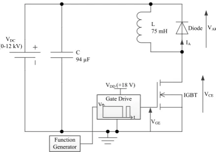
In order to characterise the reverse recovery performance of the fabricated PiN diodes, a custom-built clamped inductive switching test rig has been employed. Characteristics at temperatures up to 125 C have been obtained by heating an inert fluid in which the devices under test are submerged. The test rig is based on a chopper cell circuit, shown schematically in Figure 3. This circuit is operated in double-pulse mode which operates as follows: the gate of the IGBT is first double-pulsed on for a durationDT, allowing the inductor current to build up to the desired level. Once this current level is reached, the IGBT is turned off, forcing the inductor current to flow through the diode, turning it on, and allowing the IGBT to support a voltage across the collector-emitter junction (VCE). After a short durationto f f, the gate of the IGBT is pulsed on for a second time; due to the removal of stored charge in the PiN diode a reverse recovery current flows through the diode until it can support the reverse voltage.
DC
DD
V
t GE
CE AK
[image:5.595.188.408.291.446.2]A
Figure 3: Schematic of chopper cell circuit used for clamped inductive switching tests.
Results and discussion
Forward I-V characteristics0 1 2 3 4 5 6 0
25 50 75 100 125 150
3.81 V @ 100 A/cm2
3.75 V @ 100 A/cm2
C
ur
re
nt
d
en
si
ty
(
A
/c
m
2)
Voltage (V)
0 1 2 3 4 5 6
0 25 50 75 100 125 150
3.16 V @ 100 A/cm2
4.45 V @ 100 A/cm2
Control sample
25degC 150degC 300degC
C
ur
re
nt
d
en
si
ty
(
A
/c
m
[image:6.595.167.423.76.270.2]2) Lifetime-enhanced sample
Figure 4: Typical forward J-V characteristics for control sample (bottom) and lifetime-enhanced (top) PiN diodes.
Fig. 5 shows the typical differential on-resistance (Ron,di f f) as a function of current density of both the
lifetime-enhanced PiN diodes and the control sample PiN diodes across the temperature range 25 C to 300 C, calculated from
Ron,di f f =dJFdV (1)
In both devices, the Ron,di f f is initially high at low biases, then rapidly decreases with increasing bias
as carriers are injected from both emitters into the drift region. The lifetime-enhanced PiN diode again shows improved characteristics in comparison with the control sample PiN diode, withRon,di f f =
6.2 mW-cm2 at 100 A/cm2 and 25 C compared to 11.0 mW-cm2 for the control sample device. This equates to a decrease inRon,di f f of around 40% for the lifetime-enhanced devices.
Reverse I-V characteristics
0 25 50 75 100 125 150 0
10 20 30 40
6.2 m -cm2 @ 100 A/cm2
9.5 m -cm2 @ 100 A/cm2 Ron
,d
if
f
(
m
Ω
-c
m
2)
Current density (A/cm2)
0 25 50 75 100 125 150
0 10 20 30 40
Lifetime-enhanced sample
Control sample
4.2 m -cm2 @ 100 A/cm2
11.0 m -cm2 @ 100 A/cm2 25degC 150degC 300degC
Ron
,d
if
f
(
m
Ω
-c
m
[image:7.595.170.425.77.269.2]2)
Figure 5: Typical differential on-resistance as a function of current density for control sample (bottom) and lifetime-enhanced (top) PiN diodes.
Switching (reverse recovery) characteristics
Figure 7 shows the reverse recovery characteristics of the fabricated PiN diodes between 25 C and 125 C. It is noted that, due to the fact that the devices were fabricated with no edge termination, a relatively low DC bus voltage of 100 V has been used for these tests. Though this means that the tran-sient power losses presented here are not representative of the intended application for these PiN diodes, it still allows a valid quantitative comparison to be made between the lifetime-enhanced and the control sample devices. It is clear from this Figure that the transient characteristics of both types of device de-teriorate with increasing temperature (both the peak reverse current densityJRPand the reverse recovery timetrr increase); this is expected as the carrier lifetime, and thus the stored charge in the drift region, increases with temperature. It is also evident that the lifetime-enhanced devices exhibit marginally worse transient characteristics, indicating a longer carrier lifetime. As outlined in [14], the high-level carrier lifetimetHLcan be estimated from
tHL=2·IRP
IF ·trr (2)
whereIF is the diode forward current. Using this equation, a value of tHL of 1.2µs was extracted for the lifetime-enhanced PiN diodes; this compared to a value of 750 ns for the control sample PiN diodes, an increase of over 35%. This increased carrier lifetime meant that, the lifetime-enhanced PiN diodes had a reverse recovery chargeQrr of 67 nC, compared to 52 nC for the control sample PiN diode, an increase of around 22%. For comparison, a commercial 6.5 kV Si PiN diode was found to haveQrr=
0 20 40 60 80 100 10-10 10-9 10-8 10-7 C ur re nt d en si ty ( A /c m 2) Voltage (V)
[image:8.595.175.412.91.271.2]Lifetime-enhanced large-area device Control large-area device Lifetime-enhanced small-area device Control small-area device
Figure 6: Reverse leakage currents of lifetime-enhanced and control sample PiN diodes. Both small- and large-area device characteristics are shown.
23.6µ 23.7µ 23.8µ 23.9µ
-120 -100 -80 -60 -40 -20 0 20 Lifetime-enhanced sample VA K ( V ) Time (s) VAK JA Control sample
23.6µ 23.7µ 23.8µ 23.9µ
-120 -100 -80 -60 -40 -20 0 20 JA
25oC 75oC 125oC
VA K ( V ) VAK -375 -300 -225 -150 -75 0 75 JA ( A /c m 2) -375 -300 -225 -150 -75 0 75
25oC 75oC 125oC
JA ( A /c m 2)
Figure 7: Reverse leakage currents of lifetime-enhanced and control sample PiN diodes. Both small- and large-area device characteristics are shown.
Analysis of device power losses
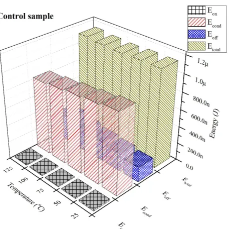
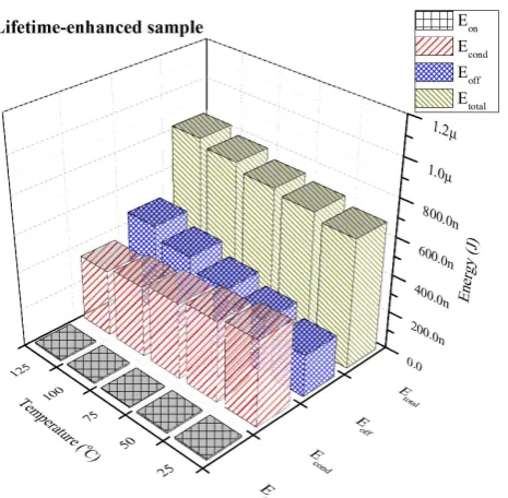
[image:8.595.163.447.396.592.2]energy losses are clearly dominated by the conduction losses, which are around 940 nJ at 25 C and de-crease to around 830 nJ at 125 C. The turn-off losses are relatively small, around 170 nJ at 25 C and increasing to around 300 nJ at 125 C. As such, the total energy losses of the control sample PiN diode remain approximately constant over the measured temperature range, at around 1.1µJ. In contrast, the conduction losses of the lifetime-enhanced PiN diode are around 450 nJ at 25 C, decreasing to around 350 nJ at 125 C. The turn-off losses are slightly lower, at around 220 nJ at 25 C, and increase to around 470 nJ at 125 C. This results in a total energy loss over the complete switching cycle of around 690 nJ at 25 C and 830 nJ at 125 C. From this analysis, it can be seen that the lifetime-enhanced PiN diodes offer an overall power loss reduction of around 40% at 25 C, and 27% at 125 C.
Figure 8: Total energy dissipated for the control sample PiN diode across the temperature range 25 C to 125 C.
Conclusions and future work
Figure 9: Total energy dissipated for the lifetime-enhanced PiN diode across the temperature range 25 C to 125 C.
References
[1] Chow T. P.: Mater. Sci. Forum Vol 778-780, pp. 1077-1082, 2014. [2] Hiyoshi T. and Kimoto T.: Appl. Phys. Expr. Vol 2, 041101, 2009. [3] Kimoto T. et al.: Phys. Stat. Sol. (b) Vol 425 no. 7, pp. 1327-1336, 2008. [4] Ichikawa S. et al.: Appl. Phys. Expr. Vol 5, 101301, 2012.
[5] Kawahara K. et al.: Mater. Sci. Forum Vol 717-720, pp. 241-244, 2012. [6] Hiyoshi T. and Kimoto T.: Appl. Phys. Expr. Vol 2, 091101, 2009. [7] Thomas S. M. et al.: Mater. Sci. Forum Vol 778-780, pp. 599-602, 2014.
[8] Fisher C. A. et al.: Accepted for publication in IEEE Trans. Semicon. Man., (notified April 2014). [9] Jennings M. R. et al.: Mater. Sci. Forum Vol 778-780, pp. 693-696, 2014.
[10] Schroder D. K.: Semiconductor Material and Device Characterization - Third Edition, John Wiley and Sons, Hoboken, NJ, USA, 2006.
[11] Fisher C. A. et al.: Mater. Sci. Forum Vol 717-720, pp. 993-996, 2012.