ISSN Online: 2327-7203 ISSN Print: 2327-7211
DOI: 10.4236/jdaip.2019.73006 Jul. 25, 2019 91 Journal of Data Analysis and Information Processing
Reconfigurable Multi-Butterfly Parallel Radix-
r
FFT Processor
Jiyang Yu, Bowen Cheng, Zongling Li, Weiwei Liu, Luyuan Wang
China Academy of Space Technology, Beijing, China
Abstract
The design of reconfigurable multi-butterfly parallel radix-r FFT (Fast Fouri-er Transform) processors is proposed. FFT is widely used in signal processing, and the application needs real-time and high performance, while most of the traditional designs are limited to the power of two, which wastes the buffers and multipliers in big data. In response to the problem, we improve the pa-rallel FFT algorithm with the design of reconfigurable control machine com-bined with buffer/multiplier, and the cost function with the input of ra-dix/number/paddling number/time consuming is deduced. Constrained with the number of buffer and multipliers, the radix and number can be computed with the optimum cost function, and the resolution space of computing per-formance and hardware cost is presented. The proposed guarantees the real-time performance with better flexibility compared with the previous lite-rature, and the comparison also suggests the effectiveness of the design.
Keywords
FFT, Reconfigurable, Multi-Butterfly, Parallel Processing
1. Introduction
The Fourier Transform is the basic algorithm for time-frequency domain processing, and the necessary tool for digital spectrum analysis. The Fast Fourier Transform (FFT), as the element theory in signal processing, is widely used in the research on electromagnetic characteristics, satellite navigation and commu-nications and radar signal processing [1]. The DSP chips were often used for the FFT real-time implementation, and nowadays the ASIC of FFT could decrease the cost and enhance the performance, which makes the great success in prac-tice.
S. A. Salehi provided pipeline architecture for FFT which is limited to the
How to cite this paper: Yu, J.Y., Cheng, B.W., Li, Z.L., Liu, W.W. and Wang, L.Y. (2019) Reconfigurable Multi-Butterfly Paral-lel Radix-r FFT Processor. Journal of Data Analysis and Information Processing, 7, 91-107.
https://doi.org/10.4236/jdaip.2019.73006
Received: April 8, 2019 Accepted: July 22, 2019 Published: July 25, 2019
Copyright © 2019 by author(s) and Scientific Research Publishing Inc. This work is licensed under the Creative Commons Attribution International License (CC BY 4.0).
DOI: 10.4236/jdaip.2019.73006 92 Journal of Data Analysis and Information Processing
power of two [2]. A normal I/O order radix-2 architecture for MIMO is shown in [3]. The pruning mechanism is applied to reduce the time consuming, while the performance is affected by points [4] [5] reduced circuit complexity for large
N-point FFT with single-path delay feedback, and the radix is also limited to 22.
The traditional FFT design, is basically restricted to the radix-2/4 and the cor-responding architectures, while the buffers and multipliers can be easily wasted for big data processing; and the previous literature often optimize the computing with constant parallel architectures, which makes it difficult to balance between performance and resources.
In previous works, [6] enhanced the performance by computing 4-channel FFT with single butterfly, which is focused on parallel data flow between mul-tiple FFTs. The in-place radix-r architecture is deduced in [1], and a constant geometry is proposed in [7].
The reconfigurable multi-butterfly parallel radix-r FFT processor is proposed, based on the improved parallel strategy. By designing configurable controller combined with hardware resources such as cache/multiplier, the parallel algo-rithm is improved. The design cost function of FFT with the input of radix, point, zero paddling and calculation time is given. In the actual design process, taking cache and multiplier resources as constraints, the optimal FFT design ar-chitecture is obtained by calculating the radix and number of points under the optimal cost function. The form of solution space is given for the computational performance and resource occupation of the design. Because of the use of pro-cessor architecture, the algorithm can be adjusted according to the availability of resources in the actual hardware design process, which not only ensures the flexibility of the design, but also guarantees the real-time requirements of paral-lel computing.
The architecture of parallel FFT processor is given in Section 2, include the internal sub-module design and connection relationship; the performance is analyzed based on the parallel architecture in Section 3, and the improved paral-lel algorithm is deduced for the designed processor; Section 4 compares the de-sign with previous literatures; Section 5 concludes.
2. The Parallel FFT Design
The point is configured by the external input interface, while the optimal radix and the parallel degree of multipliers are deduced by point. Then the parameters are used to form the FFT architecture.
DOI: 10.4236/jdaip.2019.73006 93 Journal of Data Analysis and Information Processing Figure 1. Multi-butterfly parallel radix-r FFT architecture.
Figure 2. The internal architecture of the FFT processor.
2.1. The Work Mode of FFT Processor
Processor receives external input data, and output results after calculation. The workflow is as follow: first use internal cache to receive external input data, and the register set save external input and output control information; then, calcu-late input data; at last, output results to output cache, refresh the register set, and waiting for the external data.
2.2. The Internal Architecture of FFT Processor
According to the workflow of the processor, the internal hardware structure of the processor in Figure 3 is as follow.
The processor mainly includes 8 sub-modules: 1) State Processing Unit;
2) Inline Bus;
3) Integer Processing Unit; Parameters
Comp.
Input RAM
FFT Control
Butterfly Unit(0~N-1)
Data Buffer
Output RAM Telemetry Parameters
Input
Data Input
Telemetry Output
Data Output
Result
Store Operandfetch Para.
Config. FPGA
SPU(State Processing
Unit)
ILB(Inline Bus)
IM(Input Memory)
OM(Output Memory)
IPU(Integer Processing
Unit)
MM(Middle Memory)
FPUG( Floating-point Processing Unit Group)
Data
Data
Data Data
Ctrl Ctrl
Ctrl Data
Data
Data Data
Ctrl
Data Data
FPGA
Input
Data OutputData
Reg Set Input/Output
DOI: 10.4236/jdaip.2019.73006 94 Journal of Data Analysis and Information Processing Figure 3. The internal architecture of SPU for FPGA.
4) Floating-Point Processing Unit; 5) Reg Set;
6) Input Memory; 7) Middle Memory; 8) Output Memory.
While, SPU is used to handle all state controls generated according to the al-gorithm; ILB is used to connect three-tier cache and floating-point processing units and to interact with SPU for data; IPU is used to support integer compu-ting requirements in SPU; FPUG are used for the floacompu-ting-point compucompu-ting; RS receive the input control information and internal state interaction; IM store the data input, and MM store the intermediate data, while OM store the results.
2.3. The Design of Sub-Modules
2.3.1. State Processing Unit (SPU)
The state processing unit (SPU) is used to control and command all working components. Its function is to extract the state code from the state memory, send it to the state code register, and then enter the state decoder for decoding. Ac-cording to the state code information, all the internal information needed for various operations is updated, so that all parts can coordinate their work and complete the various operations specified by the state code.
The SPU includes timing control logic, state code memory, state code register, state code decoder, state counter SC (State Count), state address register, state code pointer register SPTR and stack pointer register SP. Its internal structure is shown below.
1) Timing Control Logic
When the FPGA is started, the SPU is controlled to take out the state code and increase the state count.
Micro Operation Control
Timing Control Logic
State Code Decoder
State Code Register
State Counter
State Address Register +1/2/3
State Code Memory State
RG SPTR IPU
Stack Pointer
DOI: 10.4236/jdaip.2019.73006 95 Journal of Data Analysis and Information Processing
2) State Code Register
Store the status code currently being executed. 3) Sate Code Decoder
When the state code is fed into the state decoder, the state code is decoded by the decoder, that is, the state code is converted into various specific operations, so that the state machine can correctly perform various functions required.
4) State Address Register
To store the next status code address to be executed. When a status code is removed from the status code memory according to the SC pointing address, SC automatically adds 1/2/3 to the next status code. When reset, (SC) = 0, so the address selection of system status code must start from unit 0.
There are two ways to form a status code address: one is to execute sequen-tially, adding 1/2/3 through SC; the other is to change the sequence of execution procedures. Generally, the transfer address is formed by the transfer class status code and sent to the status code address register as the next status code address.
1) State Code Pointer Register
SPTR is used to address external data to form an external data address poin-ter.
2) Stack Pointer
SP is used to store the top address of the stack. The stack accesses data ac-cording to the “first in, last out” principle.
2.3.2. Inline Bus (ILB)
The inline bus ILB in Figure 4 updates the internal control register by decoding the data written by the SPU, and controls the data transmission between the connected components according to the value of the register. These data trans-fers in Figure 5 include:
1) Data transmission from input cache IM to intermediate cache MM; 2) Data Transfer from Intermediate Cache MM to Intermediate Cache MM; 3) Data transmission from intermediate cache MM to output cache OM; 4) Data transmission from intermediate buffer MM to floating point processing unit group FPUG;
5) Data transmission from FPUG to intermediate cache MM.
2.3.3. Integer Processing Unit (IPU)
The main function of IPU module in Figure 6 is to carry out arithmetic logic operation, and complete data transmission, calculation and bit variable processing tasks with SPU. Among them, arithmetic logic operation is mainly composed of ACC, general register B, register, Boolean processor and operation state register PSW. As shown in the figure below.
2.3.4. Floating-Point Processing Unit (FPUG)
DOI: 10.4236/jdaip.2019.73006 96 Journal of Data Analysis and Information Processing Figure 4. The internal architecture of ILB.
Figure 5. ILB inner modules data transmission indication.
each module varies according to the task requirements of parallel FFT compu-ting and the amount of remaining resources of current FPGA. Once the design requirements are identified, the number of four modules can no longer change.
2.3.5. Memory Group (MG)
Internal cache has three parts: input cache IM, intermediate cache MM and output cache OM. All three caches are dual-port RAM.
Address Decoder & ILB Inner Control Reg
MUX MUX
MUX
MUX MUX
MM
FPUG
ILB
IM OM
SPU
EN EN
EN EN
EN
MUX 1-To-3
MUX 3-To-1 EN EN
IM
MM
OM
FPUG I
II
III
[image:6.595.264.480.402.592.2]DOI: 10.4236/jdaip.2019.73006 97 Journal of Data Analysis and Information Processing Figure 6. IPU inner modules data transmission indication.
Figure 7. FPUG inner modules data transmission indication.
3. Analysis of Computational Performance
3.1. The FFT Algorithm
Suppose the point is N, where N r= M, r, M is the positive. Then, the radix-r
FFT can be represented as [1]:
( )
( )
( )
( ) ( ) ( ) ( ) ( ) ( ) ( ) ( ) ( ) ( )( )
( )
( )
1 1 1 1 1 11 1 1
0 1
0 0 0 1
1
1 1
1 0 1 1
2
1 0 1 1 1 1
1 1 1 2 1 M M M M M M
M M M
r r
r r
N N N
m
r r
r r
m N N N
r r r r r r r
m r
N N N
m p
m N
m r N
W W W
X j
X j W W W
X j W W W
X j
X j W
X j W
− − − − − − − − − × × − × × × × × × − × × × × × − × × − × × − × − − − − = ⋅ × ⋅
( )r−1p
(1) ACC B a1 a2
PSW BoolPro.
ALU Address
Control
Data
FA/FM/F
[image:7.595.264.485.298.477.2]DOI: 10.4236/jdaip.2019.73006 98 Journal of Data Analysis and Information Processing 1
1
1 m 1
M m M m
k m
j − l r − + k r − q
+ = ⋅ + − ⋅ + (2)
2 2 0 m m i i i
l − k r − −
=
=
∑
⋅ (3)1 0 M m i i i
q − −n r
=
=
∑
⋅ (4)3.2. The Parallel FFT Algorithm
For the N0-point parallel FFT (N0 is positive integer), the pre-work should be
done as:
1) Choose the current optimal radix-r and FFT point N;
2) The parallel computing flow is designed according to the number of current hardware additive multiplication.
3.2.1. Parameter Calculation
This section describes the parameter calculation method and implementation process.
1) Number of Zero Complementation Points
For the N0-point FFT, the actual number of points N of FFT is calculated by
radix-r.
0
logrN
N r= (5)
where, is the ceiling operation. The number of zeros to be paddling is
( )
log 00 rN
r r N
∆ = − (6)
where, r 2, rlogrN0
∈ . 2) Time Consuming
For the radix-r N-point FFT, time consuming is:
0 0 log 1 2.5 0 1.5 log 0 log log r r N r N r
T r r N
r N
β
β
− + = = (7)
where,
β
≥1, represents the time coefficients caused by branch jumps, data access and computing module delays in current computing systems. When the hardware structure is fixed,β
is fixed. In this paper,β
=15.7.3) Optimal Parameter Selection Based on Cost Function
In the calculation of FFT, the choice of parameters should take into account not only the calculation speed, but also the current occupancy of space resources. Therefore, the calculation time and zero-filling points should be unified plan-ning.
(
0)
γ γ
> is defined as the ratio of computing time to buffer cost. Then the total cost function isT
δ
= ∆ +γ
(8)DOI: 10.4236/jdaip.2019.73006 99 Journal of Data Analysis and Information Processing
which is
r
min(δ( )r).Examples are as follows:
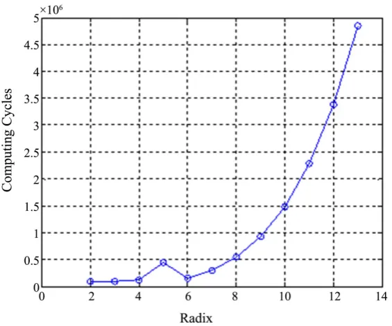
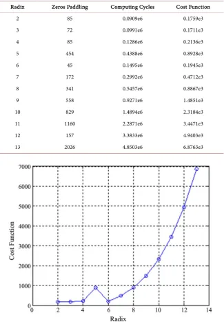
[image:9.595.232.512.219.438.2] [image:9.595.234.517.472.707.2]For the N0=171 point FFT, the zeros paddling of different radix are as in Figure 8.
The computing cycles for different radix are as in Figure 9. Suppose
γ
=10−3, then the cost function
δ
( )
r is as in Figure 10.From Table 1, the radix should be 6 according to the least zeros paddling, and should be 2 according to the minimum computing cycles. The optimal radix is 3 with the minimum cost function by generally analysis.
Figure 8. Zeros paddling comparison for different radix.
DOI: 10.4236/jdaip.2019.73006 100 Journal of Data Analysis and Information Processing Table 1. Comparison of main parameters for different radix.
Radix Zeros Paddling Computing Cycles Cost Function
2 85 0.0909e6 0.1759e3
3 72 0.0991e6 0.1711e3
4 85 0.1286e6 0.2136e3
5 454 0.4388e6 0.8928e3
6 45 0.1495e6 0.1945e3
7 172 0.2992e6 0.4712e3
8 341 0.5457e6 0.8867e3
9 558 0.9271e6 1.4851e3
10 829 1.4894e6 2.3184e3
11 1160 2.2871e6 3.4471e3
12 157 3.3833e6 4.9403e3
13 2026 4.8503e6 6.8763e3
Figure 10. Cost function with different radix.
4) The Implementation of Parameters Computing
Generally, logarithmic calculation is calculated by look-up table method and CORDIC algorithm. Because parameters can be calculated in the initialization process, the real-time requirement for parameter calculation is not high. The use of look-up table method and CORDIC algorithm will occupy a large amount of memory resources or logical resources. In this design, a simple integer logarith-mic calculation method is designed by local optimization of Taylor series expan-sion method and table lookup (256 table lookup data).
tran-DOI: 10.4236/jdaip.2019.73006 101 Journal of Data Analysis and Information Processing
scendental functions are used frequently.
The logarithm of traditional Taylor series expansion is as follows
(
)
( )
1 1ln 1 1i i
i
x ∞ − x i
=
+ =
∑
− (9)In the finite order, the closer x approaches 1, the greater the error. This leads to a high order of accuracy in order to ensure the whole range.
The derivation is as follows,
(
)
(
(
)
)
(
(
)
)
ln 1+x =ln 2 1+x 2 =ln 2 ln 1 0.5+ + x−1 (10) The following improvements are made to Taylor series expansion
(
)
(
)
(
]
(
)
(
)
(
]
ln 1 , if 0,0.5
ln 1
ln 2 ln 1 0.5 1 , if 0.5,1
x x
x
x x
+ ∈
+ =
+ + − ∈
(11)
The error of formula (11) is less than 10−4, as shown in the following Figure
11.
In the process of parameter calculation, for practical use, the point N0 is less
than 65,536, which can be expressed by 16-bit integer. At this time, the radix r
will not exceed 256, and can be expressed by 8-bit integers.
The calculation of formula (4)-(8) is mainly concentrated on the logarithm of r
obtained from N0, which is deduced as follows.
( )
(
)
00 0 0 0
0
ln ln 256 ln 256 ln ln 1
256 L
H L H
H N
N N N N
N
= + = + + +
(12) And,
0 0 ln
log
ln
[image:11.595.228.538.374.706.2]rN = Nr (13)
DOI: 10.4236/jdaip.2019.73006 102 Journal of Data Analysis and Information Processing
where, 0 0
0 1
256 LH N
N
< < , N0H <256.
For N0, the logarithm of r can be simplified into the following three steps:
1/(lnr) and lnN0H are calculated by using 8-bit 256 data lookup tables;
(
)
(
0 0)
ln 1+N L 256N H is calculated according to (11); the results plus a constant
ln256, and then are divided by lnr, which is logrN0.
3.2.2. Implementation of Parallel Computing
In the process of any radix FFT processing, the butterfly computing matrix W is first calculated, which is only related to the calculating series M and the base number r. Therefore, after calculating the parameters, W is calculated once and stored, and then only data is taken out for calculation in each butterfly calcula-tion. The r-ary reverse order of input data can ensure the correct order of settle-ment results when calculating the output. Each iteration needs to calculate N/r
butterfly calculation. Before each butterfly calculation, the twiddle factor needs to be calculated. In fact, the rotating factor can be selected in the butterfly calcu-lation matrix W. This ensures that the twiddle factor does not need additional calculation, calculates the address of the number of operands for butterfly calcu-lation, takes out r operands, and the rotating factor and the butterfly meter. The calculation matrix is multiplied separately to complete the butterfly calculation, and the storage address of the calculated butterfly results is stored.
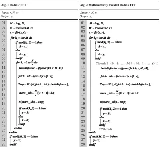
Because Singleton’s fixed structure is adopted in the design of the algorithm, X
and Y caches are used to store the input and output of each fixed structure. The pseudo code of the whole algorithm is as follows.
For the case of only one multiplier and one adder, the whole algorithm flow needs to be serially operated according to the above pseudo-code, and the calcu-lation time is as described above.
As can be seen from the above algorithm, there are two ways to improve the algorithm by using parallel computing method:
1) Parallel computation is carried out for the matrix operation in the butterfly computation of line 15 of the algorithm.
2) Parallel computing is carried out for N/r butterfly computing units.
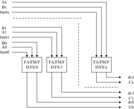
The Radix used in practical application is generally less than r = 10. Wino-grad’s second-order matrix multiplication is not suitable for use. Therefore, the traditional matrix multiplication structure (mid-product algorithm) is used for calculation.
In butterfly computing process, the r data of A(fetch_idx) are multiplied by r
twiddle factors to form the r multiplication is not suitable for use. Therefore, the traditional matrix multiplication of
r r
×
matrix and r×1 vector, needs r2mul-tiplications and r(r − 1) additions.
The parallel computing architectures are discussed as follow with the different resources:
1) When the number of multipliers nm is less than r2, and the number of
DOI: 10.4236/jdaip.2019.73006 103 Journal of Data Analysis and Information Processing
The twiddle factors must be pre-processed, and the time cost is r nm; the
time cost of matrix multiplication is max
{
2 ,(
1)
}
m a
r n r r n
−
. The parallel process applies nm threads computing. For convenience, na ≥nm+1.
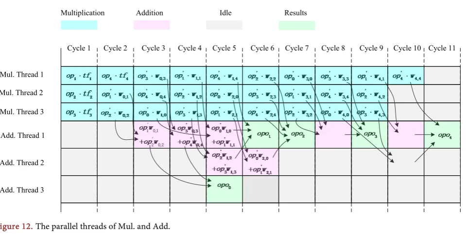
Set r = 5 and nm = 3 as the example, to illustrate the parallel design of butterfly.
Denote the operands as opi, the twiddle factors as tfi, and the product of the two
as opi′; the butterfly matrix is denoted as wi,j, and the result is opoi, where
[
]
, 0, 1
i j∈ r− . And the parallel proceed is as follow in Figure 12.
2) When the number of multipliers nm is not less than r2, and the number of
additions na is not less than r(r − 1).
The resources of adders and multipliers are greater than a fully parallel re-quirement, and multi-butterflies could be configured parallel to enhance the performance. The parallel degree is min
{
2 ,(
1)
}
m a
P= n r n r r− . When
1
a m
n ≥n + , 2
m
P= n r . Each group includes Q = N/r/P butterflies.
Improve the alg. 1, then the multi-butterfly parallel FFT alg. 2 is as follow in
Figure 13.
3.3. Analysis of Parallel Algorithm
3.3.1. Time Cost Analysis of Parallel Algorithm
According to the performance of the parallel alg. in Section 3.2.2, the gap pipe-lines in the single butterfly and the multi-butterfly are adjusted to enhance the parallelism. In each state the time cost of the butterfly is deduced as:
1) When the number of multipliers nm is less than r2, and the number of
addi-tions na is less than r(r − 1);
2
bf m N
T r n
r
= (14) 2) When the number of multipliers nm is not less than r2, and the number of
[image:13.595.62.542.485.726.2]additions na is not less than r(r − 1).
Figure 12. The parallel threads of Mul. and Add.
Cycle 1 Cycle 2 Cycle 3 Cycle 4 Cycle 5 Cycle 6 Cycle 7 Cycle 8 Cycle 9 Cycle 10 Cycle 11 Multiplication Addition Idle
Mul. Thread 1
Mul. Thread 2
Mul. Thread 3
Add. Thread 1
Add. Thread 2
Add. Thread 3
DOI: 10.4236/jdaip.2019.73006 104 Journal of Data Analysis and Information Processing Figure 13. The Alg.1 and Alg.2 for FFT.
2
bf m
N T
r n r
=
(15) Then, the total time cost is
2 2
2 2
log , if
log , if
r m m
fft
r m
m N
N r n n r
r
T N
N n r
r n r
<
= ≥ (16)
3.3.2. Resources Cost Analysis of Parallel Algorithm
The buffers of 8 modules in FFT processor are composed by block ram, while the SPU/ILB/IPU/RG/FPUG occupies the slices. The first 4 modules resources con-suming are the same with different parallel degree, and the resources of FPUG increases with parallel degree growth.
Take Xilinx Virtex-II 3000 as an example, SPU/ILB/IPU/RG costs 2973 slices; floating-point adder costs 273 slices; floating-point multiplier costs 75 slices and 4 fix-point multipliers. Then, the total costs are
2973 273 m 75 a
SrCost= + n + n (17)
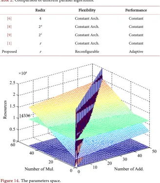
According to (17), the parameters space is depicted in Figure 14. The plane of value 14,336 represents the maximum slices in Xilinx Virtex-II 3000, and the vertical oblique plane represents boundary (na ≥nm+1). The appropriate
para-Alg. 1 Radix-r FFT
Input: r,N, x; Output: y; 01 02 03 04 05 06 07 08 09 10 11 12 13 14 15 16 17 18 19 20 21 22 23 24 25 26 27 28
Alg. 2 Multi-butterfly Parallel Radix-r FFT
01 02 03 04 05 06 07 08 09 10 11 12 13 14 15 16 17 18 19 20 21 22 23 24 25 26 27 28
Threads h (0,1,...,P-1)i(0,1,...,Q-1)
//P threads.
DOI: 10.4236/jdaip.2019.73006 105 Journal of Data Analysis and Information Processing
meters can be selected according to the space.
4. Comparison
The design method in this paper is compared with the previous literature [1] [6] [8] [9]. According to Table 2, it can be seen that the design method is flexible, the same computing performance occupies the least resources in the application process, and the optimal design parameters can be obtained according to the ac-tual situation of hardware resources.
5. Conclusion
[image:15.595.210.539.350.725.2]This paper presents a design method of configurable multi-butterfly parallel computing radix-r FFT processor. In the information processing process, FFT has a wide range of applications, large demand and high real-time requirements. The existing design methods are mainly limited to base 2/4 and the correspond-ing parallel architecture. It is easy to waste storage and multiplier resources with different number of points and multipliers under large data. In order to solve this problem, the parallel FFT algorithm is improved by designing a configurable
Table 2. Comparison of different parallel algorithms.
Radix Flexibility Performance
[6] 4 Constant Arch. Constant
[8] 2n Constant Arch. Constant
[9] 22 Constant Arch. Constant
[1] r Constant Arch. Constant
Proposed r Reconfigurable Adaptive
DOI: 10.4236/jdaip.2019.73006 106 Journal of Data Analysis and Information Processing
controller combined with hardware resources such as buffer and multiplier. The FFT design cost function with cardinality, number of points, number of zeros and computing time as input are given. In the actual design process, with the constraints of buffer and multiplier resources, the optimal FFT design architec-ture is obtained by calculating the number of points and cardinality under the optimal cost function and the form of solution space is given for the calculated performance and resource occupancy. The design method in this paper has good flexibility, and its parallel computing architecture also guarantees the real-time performance of the calculation. The comparison with the previous literature shows that the design method is effective under the same design parameters.
Acknowledgements
This work was carried out by Professor Dan Huang and Professor Zong Qi (Chongqing University of Technology). We gratefully acknowledge their invalua-ble cooperation in preparing this application note.
Conflicts of Interest
The authors declare no conflicts of interest regarding the publication of this pa-per.
References
[1] Yu, J.-Y., Huang, D., Li, X., et al. (2016) Conflict-Free Architecture for Mul-ti-Butterfly Parallel Processing In-Place Radix-r FFT. IEEE 13th International Con-ference on Signal Processing, Chengdu, 6-10 November 2016, 496-501.
[2] Salehi, S.A., Amirfattahi, R. and Parhi, K.K. (2013) Pipeline Architectures for Real-Valued FFT and Hermitian-Symmetric IFFT with Real Datapaths. IEEE Transactions on Circuits and Systems II: Express Briefs, 60, 507-511.
https://doi.org/10.1109/TCSII.2013.2268411
[3] Glittas, A.X., Sellathurai, M. and Lakshminarayanan, G. (2016) A Normal I/O Order Radix-2 FFT Architecture to Process Twin Data Streams for MIMO. IEEE Transac-tion on Very Large Scale IntegraTransac-tion Systems, 24, 2402-2406.
https://doi.org/10.1109/TVLSI.2015.2504391
[4] Ayhan, T., Dehaene, W. and Verhelst, M. (2014) A 128: 2048/1536 Point FFT Hardware Implementation with Output Pruning. 22nd European Signal Processing Conference, Lisbon, 1-5 September 2014, 266-270.
[5] Siu, T., Sham, C. and Lau, F.C.M. (2017) Operating Frequency Improvement on FPGA Implementation of a Pipeline Large-FFT Processor. 19th International Con-ference on Advanced Communication Technology, Bongpyeong, 19-22 February 2017, 5-9.https://doi.org/10.23919/ICACT.2017.7890046
[6] Yu, J.-Y., Huang, D., Li, X., et al. (2013) Four Parallel Channels Radix-4 FFT with Single Floating-Point Butterfly. Applied Mechanics and Materials, 427-429, 708-711. [7] Ma, C., Qu, X., Chen, H., et al. (2013) A Novel Conflict-Free Parallel Memory
Access Scheme for FFT Constant Geometry Architecture. Science China, Informa-tion Sciences, 4, 57-63.https://doi.org/10.1007/s11432-013-4826-5
DOI: 10.4236/jdaip.2019.73006 107 Journal of Data Analysis and Information Processing
Pruning Algorithm on FPGA. 7th International Conference on Cloud Computing,
Data Science & Engineering, Noida, 12-13 January 2017, 739-743. https://doi.org/10.1109/CONFLUENCE.2017.7943248
[9] Santhosh, L. and Thomas, A. (2013) Implementation of Radix 2 and Radix 22 FFT
Algorithms on Spartan6 FPGA. 4th International Conference on Computing,