doi:10.4236/jemaa.2011.311071 Published Online November 2011 (http://www.SciRP.org/journal/jemaa)
Efficient Analysis of Complex FSS Structure Using
the WCIP Method
Sassi Aroussi1, Latrach Latrach1, Noureddine Sboui1, Ali Gharsallah1, Abdelhafidh Gharbi1, Henry Baudrand2
1Laboratoire d’Electronique Département de Physique Faculté des Sciences de Tunis, El Manar, Tunisia; 2Laboratoire d’Electronique, Toulouse France.
Email: [email protected]
Received August 2nd, 2011; revised September 1st, 2011; accepted September 25th, 2011.
ABSTRACT
A rigorous full wave technique based on the Transverse Wave Concept Iterative Procedure (WCIP) is used to design a complex Frequency Selective Surface (FSS). These surfaces include a periodically arrangement of identical circuit. There are used as filters and reflector antenna as well as deep-space exploration for multi-frequencies operations. A simple FSS structure is studied in first stage to validate our approach. In second stage two different complex structures are studied. The good agreement between simulated and published data justify the design procedure.
Keywords: FSS, WCIP, Wave,2D-FFT Algorithm
1. Introduction
Frequency Selective Surfaces (FSSs), which find wide-spread applications as filters for microwaves and optical signals, have been the subject of extensive studies in re-cent years [1-4]. These surfaces include a periodically arranged metallic patch elements or aperture elements within a metallic screen and exhibit total reflection (pat- ches) or Transmission (apertures) in the neighborhood of the element resonance [1]. Their performances depend on the substrate characteristics, element type, dimensions and the spacing between elements.
The response parameters are predicted by analyzing the surface using different techniques [5-7]. However, the small dimensions of the circuit produce some prob-lems in result precisions. Thus, the coupling conditions between the different elements must be taken into ac-count. Then, the efficiency of used method, their memory consumption and time requirement are usually made these methods unsuitable for optimization.
This paper presents the analysis of simple and com-plex passive FSS by the iterative method (WCIP). The WCIP technique takes the advantage of simplicity in its procedure based on Fast Modal Transform (FMT) in passage between spatial and spectral domain [8,9]. In addition, there is no matrix inversion was required and the convergence was insured independently of the circuit complexity. Further, there is unlimited shapes of circuit
are imposed [10]. The simulation results are validated with those calculated with HFSS commercial code and recently published experimental results.
2. Theory: WCIP Formulation
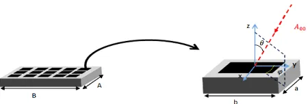
The general Frequency Selective Surface structure is depicted in Figure 1. The circuit interface is constituted
of two sub domains: metal and dielectric. It is deposed on homogeneous dielectric substrate with thickness h and permittivityr.
WCIP method is based on the full wave transverse wave formulation and the on collection of information at the interfaces. A multiple reflection procedure is started using initial conditions and stopped once convergence which is achieved. Two related operators incidented wa- ves and scattered waves in the spatial domain and in the spectral domain governs the iterative procedure. They are: the scatting operator S and the reflection .
[image:1.595.309.534.628.704.2]We consider the printed circuit, the wave concept is
FMT
[image:2.595.59.288.86.235.2]FMT–1
Figure 2. Iterative process.
introduced to express the boundary conditions on the interface Ω (Figure 2).
The incident waves Ai and the scattered waves Bi are
calculated from the tangential electric and magnetic fields Eiand Hias:
0
0
1
2 i i
Z Z
i i
A E J
00
1
2 Z i Z i
i i
B E J (1)
where i indicates the medium 1 or 2 corresponding to a given interface . Z0i is the characteristic impedance of the same medium i and Jibeing the surface current
density vector given as:
i i
J H n (2)
with n being the outward vector normal to the interface.
Thus, the tangential electric and magnetic fields can be calculated from:
0i(
Z
i i i)
E A B (3.1)
0i(
Z
i i i)
J A B (3.2)
The scattered waves are related to the incident waves as: S 1 2 2 1 B A
B A (4) S is a scattering operator defines in the spatial and it accounts for the boundary conditions. The scattered wa- ves Bi will be reflect to generate the incident waves for
the next iteration but after adding the incident source waves A0:
0
1 1 0
2 2
A B A
A B (5)
being the reflection operator and it is defined in
the s
rator pectral domain.
2.1. Scattering Ope
i
S Determination
the ad-
e
(6.1)
(6.2)
The boundary conditions on the metal domain Two domains characterizing interface of a lo ed FSS are: the dielectric domain and the m tal domain. They can be represented using Heaviside unit steps as:
1 on the dielectric
0 otherwise
D H
1 on the metal 0 otherwise
M H
M H
are:
1 2 0
E E (7)
Replacing (3) in (7) results in:
01( ) 02(
Z A1B1 Z A2B2)0 (8) The metal domain scattering operator SMis given in e terms of the metallic domain generator HM by:
0 H th 0 M M M S H
(9)
In the dielectric domain, the boundary conditions be satisfied on the interface are:
0
J J J
1 2
1 2
tot
E E (10)
Using (3) and (10), and defining N Z01 Z02.thus,
the dielectric domain scattering operator SD can be
given terms of the dielectric generator HD as:
2
1 N 2
2 2 2 2 2 1 1 2 1 1 1 D D D D D H H N N s N H H N N (11)
In the lumped elements domain, the boundary to be ve- rified is given by:
( )
s
Z
1 2 1 2
E E J J (12)
Then, the total scatting operator S is given as:
M D
SS S (13) 2.2. Reflection Operator Dete
des where rmination
The modes are decoupled in the domain of mo
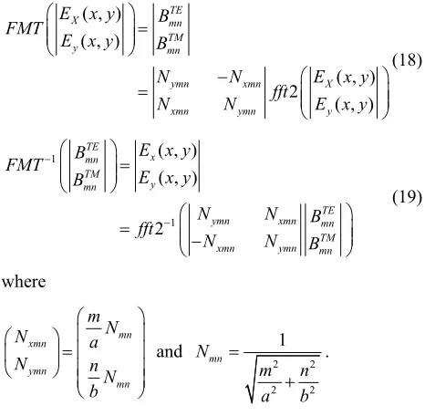
each mode is characterized by its own reflection coeffi- cient, the need to pass to spectral domain is necessary. To enable this operation, a transform known as the Fast Modal Transform FMT defined and to go back to spa-tial domain, FMT1 is will be used.
given by: 0 0 1 1 i imn imn i imn Z Y Z Y
(14)
where Yimn is the admittance of the mn mode at the
me-dium i and α stands for the modes TE or TM.
When no closing ends exist, Yimn can be calculated
by [5,6]: 0 TM ri imn mn jw Y y
(15)
0 TE mn imn y Y jw
(16)
being the propagation constant of the medium i and
mn
y
it is given by:
2 2
2 0
2π 2π
mn ri
m n
y k
A B
(17)
0, ri and 0
ve of the medi
are permittivity of the vacuum, the rela-ti
dal Transform FMT
um i and the permeability of the vacuum respectively.
2.3. Fast Mo
The FMT FMT1 pair permits to go from spatial
to the spectral
main domain and back to the spatial domain [7]. It is summarized in the following two equations.
( , ) TE
E x y B
( , ) ( , ) 2 ( , ) X mn TM y mn
ymn xmn X
xmn ymn y
FMT
E x y B
N N E x y fft
N N E x y
(18) 1 1 ( , ) ( , ) 2 TE x mn TM y mn TE
ymn xmn mn
TM xmn ymn mn
E x y B
FMT
E x y B
N N B fft
N N B
(19) where mn xmn ymn mn mN N a N n N b and 2 2 2 2 1 mn N m n a b .
3. Applications
our method, we consider at first the In order to validate
structure of Figure 3. The dashed lines are the
hypo-thetical periodic walls assumed to reduce the analysis to that of the repeated unit cell with dimensions of a = 3
mm, b = 3 mm, h1 = 4 mm, h2 = 3.125 mm, εr2 = 2.6, εr1 =
1. The TE01 mode is used as excitation and the iterative process is stopped after 200 iteration. The results of our method are compared to those calculated with HFSS and depicted in Figures 4 and 5 for the reflected and the
[image:3.595.309.541.179.309.2]transmitted respectively coefficient. In the two cases, a good agreement is obtained between results.
[image:3.595.326.518.265.706.2]Figure 3. Geometry of unit cell.
Figure 4. Reflection coefficient.
[image:3.595.339.510.340.513.2] [image:3.595.56.289.425.653.2]For the s onator cir-cu
nd example is represented in Figures 8 and 10
econd application, we consider res
[image:4.595.309.537.87.237.2] [image:4.595.64.279.258.359.2]its optimized by the genetic algorithm [8] included in WR90 waveguide (a = 22.86 mm, b = 10.16 mm) The TE01 mode is used as excitation and the iterative process is stopped after 200 iteration. This circuit is used as a filter. Two different configurations of the filter are used.
Figure 6 show the first form of the filter. The
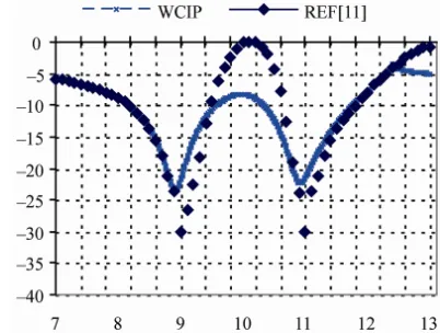
transmis-sion parameter is depicted in Figure 7. As shown in Fig-ure 7, the WCIP results are in agreement with published
data [11]. The seco
and its response is depicted in Figures 9 and 11. In
this figures, the WCIP results are compared to those of
[image:4.595.318.528.260.381.2]Figure 6. Waveguide filter with frequency selective surfac s. e
Figure 7. Transmission response as function of frequency.
Figure 8. Waveguide filter with frequency selective surfac es (FSS2).
[image:4.595.64.282.391.536.2]Figure 9. Transmission response as function of frequency.
[image:4.595.319.520.421.573.2]Figure 10. Waveguide filter with frequency selective s urfa-ces (FSS3).
Figure 11. Transmission response as function of freque y.
ublished data [11]. Then, we can conclude that the two
, the Wave concept Iterative Method
nc
p
results are agreed in pass band.
4. Conclusions
All over this paper
[image:4.595.62.282.566.693.2][1] R. Mitter, C. Technique for An-alyzing Frequ s,” Proceedings of
REFERENCES
H. Chan and T. Cwik, “ encey Selective Surfacethe IEEE, Vol. 76, No. 12, 1988, pp. 1593-1615.
[2] B. A. Munk, “Frequency Selective Surfaces: Theory and Design,” Wiley, New York, 2000.
doi:10.1002/0471723770
[3] D. J. D. H. Werver, A. Monorchio,
Wilhelm, “The Design Synthesis of Multi-Band Artificial L. Lanuzza and M. J. Magnetic Conductors Using High Impedance Frequency Selective Surfaces,” IEEE Transactions on Antennas and Propagation, Vol. 53, No. 1, 2005, pp. 8-17.
doi:10.1109/TAP.2004.840540
[4] D. Hokim and J. I. Choi, “Design of a Multi quency Selective Surface,” ETR
-Band Fre-I Journal,Vol. 28, No. 4,
t Focusing for a Bi-Layer Planar FSS
strip Phased-Array Antennas,” IEEE Transac-2006, pp. 506-508.
[5] N. Bliznyuk and N. Engheta, “Numerical Study of Po-larization Dependan
Reflective at Millimeter Wave Length,” Microwave and Optical Technology Letters, Vol. 40, No. 5, 2004, pp. 361-365.
[6] A. K. Bhattacharyya, “A Numerical Model for Multilay-ered Micro
tions on Antennas and Propagation,Vol. AP-44, No. 10, 199, pp. 1386-13936. doi:10.1109/8.933485
[7] M. Bozzi, L. Perregrini, J. Weinzierl and C. Winnewisser,
.
Latrach, A. Gharsallah, H. Baudrand and A. “Efficient Analysis of Quasi-Optical Filters by a Hybrid MoM/BI-RME Method,” IEEE Transactions on Antennas and Propagation,Vol. 49, No. 7, 2001, pp. 1054-1064. [8] L. Latrach, N. Sboui, A. Gharsallah, A. Gharbi and H
Baudrand, “A Design and Modelling of Microwave Ac-tive Screen Using a Combination of the Rectangular and Periodic Waveguide Modes,” Journal of Electromagnetic Waves and Applications, Vol. 23, No. 11-12, 2009, pp. 1639-1648.
[9] N. Sboui, L.
Gharbi, “A 2D Design and Modeling of Microstrip Struc-tures on Inhomogeneous Substrate,” RF and Microwave Computer-aidedvEngineering, Vol. 19, No. 3, 2009, pp. 346-353. doi:10.1002/mmce.20354
[10] Sboui, N., A. Gharsallah, A. Gharbi and H. Baudrand,
and H. Shigesawa, “Global Modelling of Microwave Active Circuits by an Efficient Iterative Procedure,” International Journal of
RF and Microwave Computer-Aided Engineering, Vol.
148, No. 3, 2001, pp. 209-212. [11] M. Ohira, H. Deguchi, M. Tsuji