Abstract—A closed-loop scheme of a high-gain multiphase switched-capacitor coupled-inductor (MSCCI) converter is proposed by combining a phase generator and pulse-width- modulation-based (PWM-based) gain compensator for step-up DC-DC conversion and regulation. The power part between source V S and output V O contains a three-stage serial-parallel switched-capacitor (SC) circuit plus a coupled-inductor device, and it raises the voltage gain up to 4[(n+1)+(1+nD)/(1-D)] at most, where D means the duty cycle of PWM and n is trun ratio of coupled inductor. Practically, this MSCCI can boost the voltage gain up to 44 when D=0.5, n=4. Further, the PWM technique is adopted not only to enhance the output regulation for the compensation of the dynamic error between the practical and desired outputs, but also to reinforce output robustness against source or loading variation. Finally, the closed-loop MSCCI is designed by SPICE and simulated for some cases: steady-state and dynamic responses. All results are illustrated to show the efficacy of the proposed scheme.
Index Terms—high-gain, pulse-width-modulation, step-up converter, multiphase switched-capacitor coupled-inductor.
I. I NTRODUCTION
Recently, with the rapid development of power electronics, the step-up DC-DC converters are emphasized more widely for the electricity-supply applications, such as lighting device, smart phone, medical equipment. General speaking, these power electronics converters are always required for a small volume, a light weight, a high efficacy, and a better regulation capability.
The switched-capacitor converter (SCC), possessed of the charge pump structure, is one of solutions to DC-DC power conversion because it has only semiconductor switches and capacitors. Unlike traditional converters, the inductor-less SCC has light weight and small volume. Up to now, many types have been suggested [1], [2], and some well-known topologies are presented, e.g. Dickson charge pump, Ioinovici SC. In 1976, Dickson charge pump was proposed with a two-phase diode-capacitor chain [3], [4], but it has the drawbacks of fixed gain and large device area.
In the 1990s, Ioinovici proposed a SCC with two symmetrical capacitor cells, and presented a current-mode SCC [5], [6]. In 1997, Zhu and Ioinovici performed a comprehensive steady-state analysis of SCC [7]. In 1998, Mak and Ioinovici suggested a high-power-density SC inverter [8]. In 2004, Chang presented a current-mode SC inverter [9]. In 2009, Tan et al. proposed the modeling and Manuscript received December 1, 2016. This work is supported in part by Ministry of Science and Technology of Taiwan, R.O.C., under Grant MOST 105-2221-E-324-011.
Yuen-Haw Chang and En-Ping Jhao are with the Department and Graduate Institute of Computer Science and Information Engineering, Chaoyang University of Technology, Taichung, Taiwan, R.O.C. Post code:
413. (e-mail: [email protected], [email protected]).
design of SCC by variable structure control [10]. In 2011, Chang proposed an integrated step-up/down SCC (SCVM/
SCVD) [11]. In 2013, Chang proposed a gain/efficiency- improved serial-parallel switched-capacitor converter (SPSCC) by combining an adaptive-conversion-ratio (ACR) and pulse-width-modulation (PWM) control [12]. In 2016, Chang proposed a switch-utilization-improved switched- inductor switched-capacitor converter with adapting stage number (SISCC) is proposed by phase generator and PWM control [13].
For a higher voltage gain, it is one of the good ways to utilize the device of coupled-inductor. Nevertheless, the stress on transistors and the volume of magnetic device must be considered. In 2011, Berkovich et al. proposed a switched-coupled inductor cell for DC-DC converter with very large conversion ratio [14]. In 2015, Chen et al.
proposed a novel switched-coupled-inductor DC-DC step- up converter via adopting a coupled inductor to charge a switched capacitor for making voltage gain effectively increased. Not only lower conduction losses but also higher power conversion efficiency is benefited from a lower part count and lower turn ratio [15]. Here, we try to combine a three-stage SC circuit with one coupled-inductor to propose a closed-loop MSCCI converter for realizing a high-gain conversion as well as enhancing the regulation capability.
II. C ONFIGURATION OF MSCCI
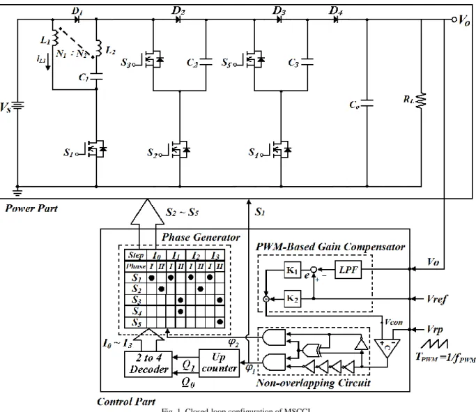
Fig. 1 shows the overall circuit configuration of MSCCI step-up converter, and it contians two major parts:
power part and control part for achieving the high-gain step-up DC-DC conversion and closed-loop regulation.
A. Power part
The power part of MSCCI is shown in the upper half of
Fig. 1, and is composed of a multiphase serial-parallel
switched-capacitor circuit plus combining a coupled-
inductor device. The converter contains one coupled-
inductor (L 1 ,L 2 ) with the turn ratio n (n=N 2 /N 1 ), five
switches (S 1 -S 5 ), one clamping capacitor (C 1 ), two pumping
capacitors (C 2 -C 3 ), one output capacitor (C O ) and four
diodes (D 1 -D 4 ), where C 2 and C 3 has the same capacitance
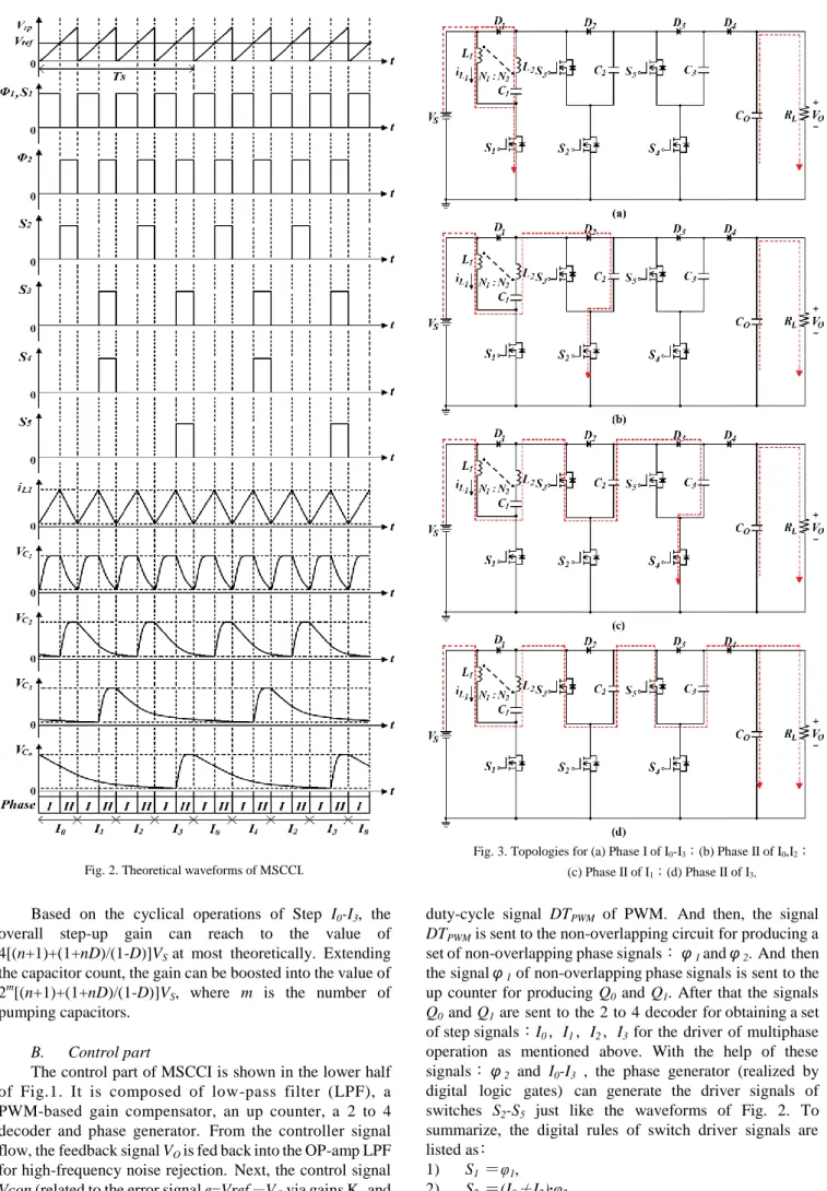
C (C 2 =C 3 =C). Fig. 2 shows the theoretical waveforms of
MSCCI in one switching cycle T PWM (T PWM =1/f PWM , f PWM :
switching frequency of PWM). A cycle T S includes four
steps (Step I 0 , I 1 , I 2 , I 3 ), and each step has two phases (Phase
I and Phase II) with the different time duration: DT PWM and
(1-D)T PWM , where D is the duty cycle of PWM control. The
operations for Step I 0 -I 3 are described as follows.
Fig. 1. Closed-loop configuration of MSCCI.
(i) Step I 0 : (a) Phase I:
Let S 1 turn on, and the others be off. Then, the diodes D 1 is turned on, and the diodes D 2 -D 4 are all off. The current-flow path is shown in Fig.
3(a). The inductor L 1 is charged by source V S , and the energy is simultaneously transfered from the first side of the coupled-inductor to the secondary side for making the voltage across L 2 being nV S . And then, the inductor L 2 is discharged in series together with V S . to have the steady-state voltage of C 1 towards the value of (n+1)V S . At the same time, output capacitor C O just stands alone to supply load R L .
(b) Phase II:
Let S 2 turn on, and the others be off. The diodes D 2 is on, and D 1 , D 3 , D 4 are all off. The current-flow path is shown in Fig. 3(b). The capacitors C 2 is charged by V S in series together with V L1 , V L2 and V C1 , i.e. transferring the previous energy stored in L 1 , L 2 and C 1 into C 2 . Thus, the steady-state voltage of V C2 can reach towards the value of [(n+1)+(1+nD)/(1-D)]V S . At the same time, output capacitor C O just stands alone to supply load R L .
(ii) Step I 1 :
(a) Phase I:Identical to Phase I of Step I 0 . (b) Phase II:
Let S 3 , S 4 turn on, and the others be off. The diode D 3 is on, and D 1 , D 2 , D 4 are off. The current-flow path is shown in Fig. 3(c). The capacitors C 3 are charged by V S in series together with V L1 , V L2 , V C1 , V C2 . i.e. transferring the previous energy stored in L 1 , L 2 C 1 and C 2 into C 3 . Thus, the steady-state voltage of V C3 can reach towards the value of 2V C2 .
(iii) Step I 2 :
(a) Phase I:Identical to Phase I of Step I 0 . (b) Phase II:Identical to Phase II of Step I 0 . (iv) Step I 3 :
(a) Phase I:Identical to Phase I of Step I 0 . (b) Phase II:
Let S 3 , S 5 turn on, and the others be off. The
diode D 4 is on, and D 1 , D 2 , D 3 are off. The
current-flow path is shown in Fig. 3(d), and is
going from source V S , through L 1 , L 2, C 1 , C 2 , C 3 ,
to output capacitor C O and load R L . This
topology has the connection in series of V S ,V L1 ,
V L2 , V C1 , V C2 and V C3 in order to provide a higher
voltage for transferring the energy into the
output terminal (C O and R L ).
Fig. 2. Theoretical waveforms of MSCCI.
Based on the cyclical operations of Step I 0 -I 3 , the overall step-up gain can reach to the value of 4[(n+1)+(1+nD)/(1-D)]V S at most theoretically. Extending the capacitor count, the gain can be boosted into the value of 2 m [(n+1)+(1+nD)/(1-D)]V S , where m is the number of pumping capacitors.
B. Control part
The control part of MSCCI is shown in the lower half of Fig.1. It is composed of low-pass filter (LPF), a PWM-based gain compensator, an up counter, a 2 to 4 decoder and phase generator. From the controller signal flow, the feedback signal V O is fed back into the OP-amp LPF for high-frequency noise rejection. Next, the control signal Vcon (related to the error signal e=Vref - V O via gains K 1 and K 2 ) is compared with the ramp Vrp to generate the
Fig. 3. Topologies for (a) Phase I of I 0 -I 3 ;(b) Phase II of I 0 ,I 2 ; (c) Phase II of I 1 ;(d) Phase II of I 3 .
duty-cycle signal DT PWM of PWM. And then, the signal DT PWM is sent to the non-overlapping circuit for producing a set of non-overlapping phase signals:φ 1 andφ 2 . And then the signalφ 1 of non-overlapping phase signals is sent to the up counter for producing Q 0 and Q 1 . After that the signals Q 0 and Q 1 are sent to the 2 to 4 decoder for obtaining a set of step signals:I 0 ﹐I 1 ﹐I 2 ﹐I 3 for the driver of multiphase operation as mentioned above. With the help of these signals:φ 2 and I 0 -I 3 , the phase generator (realized by digital logic gates) can generate the driver signals of switches S 2 -S 5 just like the waveforms of Fig. 2. To summarize, the digital rules of switch driver signals are listed as﹕
1) S 1 =φ 1 ,
2) S 2 =(I 0 + I 2 )·φ 2 ,
3) S 3 =(I 1 + I 3 )·φ 2 ,
(a) (d)
(b) (e)
(c) (f)
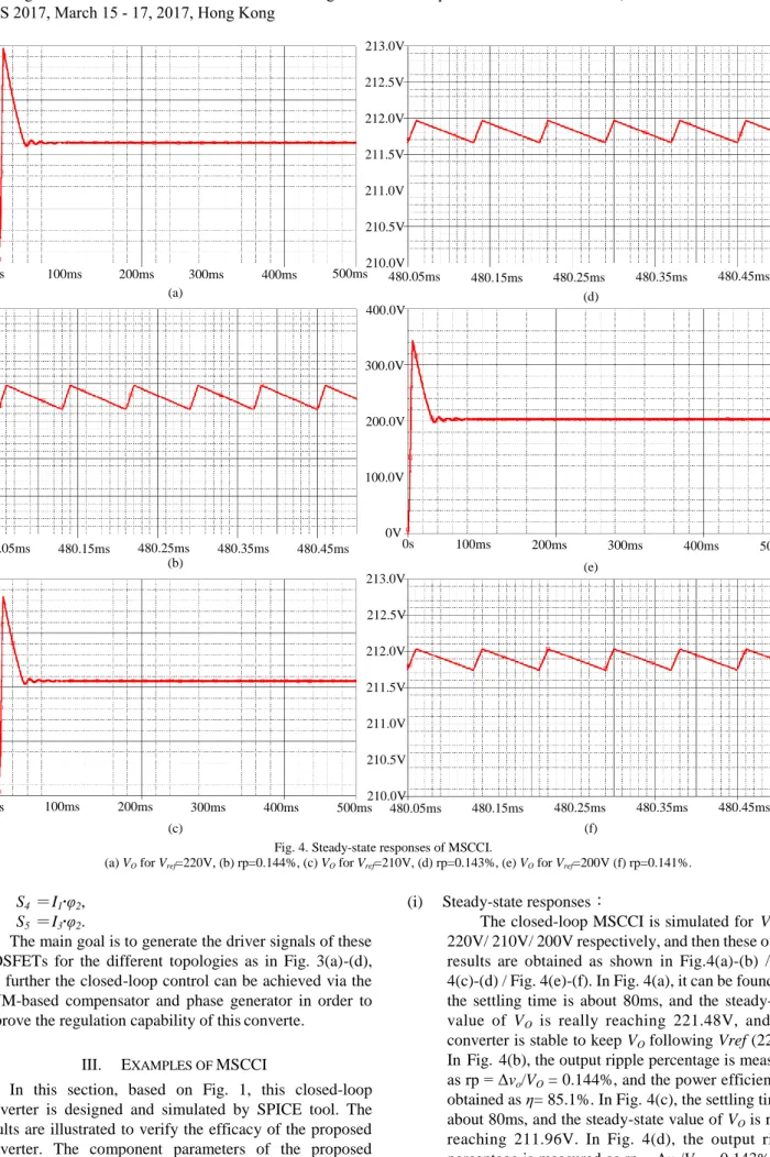
Fig. 4. Steady-state responses of MSCCI.
(a) V O for V ref =220V, (b) rp=0.144%, (c) V O for V ref =210V, (d) rp=0.143%, (e) V O for V ref =200V (f) rp=0.141%.
4) S 4 =I 1 ·φ 2 , 5) S 5 =I 3 ·φ 2 .
The main goal is to generate the driver signals of these MOSFETs for the different topologies as in Fig. 3(a)-(d), and further the closed-loop control can be achieved via the PWM-based compensator and phase generator in order to improve the regulation capability of this converte.
III. E XAMPLES OF MSCCI
In this section, based on Fig. 1, this closed-loop converter is designed and simulated by SPICE tool. The results are illustrated to verify the efficacy of the proposed converter. The component parameters of the proposed converter are listed in Table I. This converter is preparing to supply the standard load R L =500Ω. For checking closed-loop performances, some topics will be simulated and discussed, including: (i) Steady-state responses, (ii) Dynamic responses.
(i) Steady-state responses:
The closed-loop MSCCI is simulated for Vref = 220V/ 210V/ 200V respectively, and then these output results are obtained as shown in Fig.4(a)-(b) / Fig.
4(c)-(d) / Fig. 4(e)-(f). In Fig. 4(a), it can be found that the settling time is about 80ms, and the steady-state value of V O is really reaching 221.48V, and this converter is stable to keep V O following Vref (220V).
In Fig. 4(b), the output ripple percentage is measured as rp = Δv o /V O = 0.144%, and the power efficiency is obtained as η= 85.1%. In Fig. 4(c), the settling time is about 80ms, and the steady-state value of V O is really reaching 211.96V. In Fig. 4(d), the output ripple percentage is measured as rp = Δv o /V O = 0.143%, and the power efficiency is obtained as η=85.59%. In Fig.
4(e), the settling time is about 80ms, and the steady-state value of V O is really reaching 203.03V.
0V 100ms 200ms 300ms 400ms 500ms
400.0V
300.0V
200.0V
100.0V
0V 100ms 200ms 300ms 400ms 500ms
100ms 200ms 300ms 400ms 500ms
400.0V
300.0V
200.0V
100.0V
480.05ms 480.15ms 480.25ms 480.35ms 480.45ms 219.5V
220.0V 220.5V 221.0V 221.5V 222.0V 222.5V
210.0V
480.05ms 480.15ms 480.25ms 480.35ms 480.45ms 0s
0s
0s 210.0V
210.5V 211.0V 211.5V 212.0V 212.5V 213.0V
480.05ms 480.15ms 480.25ms 480.35ms 480.45ms
0V
(a) (d)
(b) (e)
(c) (f)
Fig. 5. Dynamic response of MSCCI.
(a) R L =500Ω→250Ω→500Ω, (b) V O (Case I); (c) V ref =220V→200V→220V, (d) V O (Case II); (e) V S =4.8+0.2sin(21000t) V, (f) V O (Case III).
In Fig. 4(f), the output ripple percentage is measured as rp = Δv o /V O = 0.141%, and the power efficiency is obtained as η= 85.98%. These results show that the closed-loop MSCCI converter has a high voltage gain and a good steady-state performance.
(ii) Dynamic responses:
Since the voltage of battery is getting low as the battery is working long time, or the bad quality of battery results in the impurity of source voltage, such a voltage variation should be considered as well as loading variation.
(a) Case I:(loading variation)
Assume that R L is 500Ω normally, and it changes from 500Ω to 250Ω. After a short period of 180ms, the load recovers from 250Ω to 500Ω, i.e. R L =500Ω→250Ω→500Ω as in Fig.5(a). Fig.5(b) shows the transient during waveform of V O at the moment of loading
variations. It is found that V o has a small drop (1.5V) at R L : 500Ω→250Ω (double loading).
The curve shape becomes thicker during the period of the heavier load, i.e. the output ripple becomes bigger at this moment. Even though the double loading happens, it can be found that V O still follows Vref (220V).
(b) Case II:(reference variation)
Assume that Vref is 220V normally, and it suddenly changes from 220V to 200V. After a short period of 180ms, the Vref recovers from 200V to 220V, i.e. Vref=220V→200V→220V as in Fig. 5(c). The waveform of V O is obtained in the Fig. 5(d). It is found that V O is still following Vref via the closed-loop compensation, even though Vref has a voltage drop of about 18.45V.
250Ω
120ms 200ms 280ms 360ms 440ms
205V 210V 215V 220V 225V 230V 235V
120ms 200ms 280ms 360ms 440ms
200V 205V 210V 215V
120ms 200ms 280ms 360ms 440ms
190V
120ms 200ms 280ms 360ms 440ms
220V
4.60V 4.70V 4.90V 5.00V 5.20V
120ms 200ms 280ms 360ms 440ms
210V 215V 220V 225V 230V
120ms 200ms 280ms 360ms 440ms
4.80V
5.10V
Load resistor (R L ) 500Ω
Fig. 6. Prototype circuit of MSCCI.
(c) Case III:(source variation)
Assume that V S is the DC value of 4.8V and extra plus a sinusoidal signal disturbance of 0.4V P-P as in the Fig. 5(e), and then the waveform of V O is obtained in the Fig. 5(f) (Vref=220V). Clearly, by using the closed-loop control, V O is still keeping on Vref in spite of source disturbance.
IV. C ONCLUSIONS
A closed-loop high-gain MSCCI converter is proposed by combining a phase generator and PWM-based gain compensator for step-up DC-DC conversion and regulation.
(MSCCI: V S → V O : 2 m [(n+1)+(1+nD)/(1-D)]V S ). Finally, the closed-loop MSCCI converter is designed and simulated by SPICE for some cases: steady-state and dynamic responses. The advantages of the proposed scheme are listed as follows. (i) In the MSCCI, the large conversion ratio can be achieved with five switches, three capacitors, and one coupled-inductor for a step-up gain of 44 or above.
(ii) As for the higher step-up gain, it is easily realized through increasing the turn ratio or extending the number of pumping capacitors. (iii) The PWM technique is adopted here not only to enhance output regulation capability for the different desired output, but also to reinforce the output robustness against source/loading variation. At present, the prototype circuit of the proposed converter is implemented in the laboratory as shown the photo in Fig. 6. Some experimental results will be obtained and measured for the verification of the proposed converter.
pp. 1231–1240, Aug. 1997.
[5] O. C. Mak, Y. C.Wong, and A. Ioinovici, “Step-up DC power supply based on a switched-capacitor circuit,” IEEE Trans. Ind.
Electron., vol. 42, no. 1, pp. 90–97, Feb. 1995.
[6] H. Chung and A. Ioinovici, “Switched-capacitor-based DC-to-DC converter with improved input current waveform,” in Proc. IEEE Int. Symp. Circuits Syst., Atlanta, GA, USA, 1996, pp. 541–544.
[7] G. Zhu and A. Ioinovici, “Steady-state characteristics of switched-capacitor electronic converters,” J. Circuits, Syst., Comput., vol. 7, no. 2, pp. 69–91, 1997.
[8] O. C. Mak and A. Ioinovici, “Switched-capacitor inverter with high power density and enhanced regulation capability,” IEEE Trans. Circuit Syst. I, vol. 45, pp. 336–347, Apr. 1998.
[9] Y.-H. Chang, “Design and analysis of power-CMOS-gate-based switched-capacitor boost DC-AC inverter,” IEEE Trans. Circuits Syst. I: Fundamental Theory Appl., vol. 51, no. 10, pp. 1998–2016, Oct. 2004.
[10] S.-C. Tan, S. Bronstein,M. Nur, Y.M. Lai, A. Ioinovici, and C. K.
Tse, “Variable structure modeling and design of switched-capacitor converters,” IEEE Trans. Circuits Syst. I: Reg.
Papers, vol. 56, no. 9, pp. 2132–2141, Sep. 2009.
[11] Y.-H. Chang, “Variable-conversion-ratio switched-capacitor- voltage-multiplier/divider DC-DC converter,” IEEE Trans.
Circuits Syst. I: Reg. Paper, vol. 58, no. 8, pp. 1944–1957, Aug.
2011.
[12] Y.-H. Chang, “A gain/efficiency-improved serial-parallel switched- capacitor step-up DC–DC converter,” IEEE Trans. Circuits Syst. I:
Reg. Paper, vol. 60, no. 10, pp. 2799–2809, Oct. 2013.
[13] Y.-H. Chang, Y.-J. Chen, “A switch-utilization-improved switched-inductor switched-capacitor converter with adapting stage number”, International Journal of Circuit Theory and Applications, vol. 44, iss. 3, pp. 709-728, Mar. 2016.
[14] B. Axelrod and Y. Berkovich, “Switched-coupled inductor cell for DC–DC converters with very large conversion ratio,” IET Power Electron., vol. 4, no. 3, pp. 309–315, Mar. 2011.
[15] S.-M. Chen, “A novel switched-coupled-inductor DC-DC step-up converter,” IEEE Trans. Industry Applications., vol. 51, no. 1, pp.
309-314, Jan. 2015.