AENSI Journals
Australian Journal of Basic and Applied Sciences
ISSN:1991-8178Journal home page: www.ajbasweb.com
Corresponding Author: Mariani Idroas, Faculty of Petroleum and Renewable Energy Engineering, Universiti Teknologi Malaysia, 81310 Johor Bahru, Johor, Malaysia.
Tel: 607-5535512 E-mail: [email protected],
Data Acquisition for Optical Tomography System based on Complementary Metal
Oxide Semiconductor Area Image Sensor
1
M. Suhaila Najib, 2Mariani Idroas, 3M. Nasir Ibrahim
1Universiti Teknikal Malaysia Melaka,Hang Tuah Jaya, 76100 Durian Tunggal, Melaka,Malaysia.
2Faculty of Petroleum & Renewable Energy Engineering, Universiti Teknologi Malaysia, 81310 UTM Johor Bahru, Johor. 3Faculty of Electrical Engineering, Universiti Teknologi Malaysia, 81310 UTM Johor Bahru, Johor.
A R T I C L E I N F O A B S T R A C T Article history:
Received 30 September 2014 Received in revised form 17 November 2014 Accepted 25 November 2014 Available online 6 December 2014
Keywords:
Data acquisition, CMOS area image sensor, Arduino Mega 2560
This paper describes the development of a low power consumption and low cost data acquisition system (DAQ), which is used to capture images for optical tomography system. The system used a Complementary Metal Oxide Semiconductor (CMOS) image sensor as an optical sensor. Arduino Mega 2560 is used as the control circuit to produce its own DAQ. To test the functionality of the system, several tests were conducted to capture the shape of the object. The results showed that the images of the objects were successfully being reconstructed. With 5.2µm2 of pixel size, this will produce high resolution reconstructed image for the optical tomography.
© 2014 AENSI Publisher All rights reserved. To Cite This Article: M. Suhaila Najib, Mariani Idroas, M. Nasir Ibrahim, Data Acquisition for Optical Tomography System based on Complementary Metal Oxide Semiconductor Area Image Sensor. Aust. J. Basic & Appl. Sci., 8(23): 8-14, 2014
INTRODUCTION
Process tomography interrogates the internal behavior of a process vessel in order to obtain a rigorous cross
sectional images of the its internal characteristics (Dickin et al., 1992)(Ibrahim, Green, Dutton, & Rahim,
2000)(R. H. A. Rahim, 2004). A process tomography consists of a lighting system, a sensoring unit that captures the internal behavior inside the process vessel and an imaging system to obtain its internal characteristics. A lighting system is vital to ensure that the optical sensor receives sufficient light, thus produce accurate data for image reconstruction. In this research, a Complementary Metal Oxide Semiconductor (CMOS) image sensor is used as an optical sensor. Idroas (2010) used charged couple device (CCD) image sensor, Schleicher (2008)
used optical fiber (Schleicher et al., 2008), Abdul Rahim (2005) adopted photo-detector (R. A. Rahim, Chan,
Pang, & Leong, 2005) and Abdul Rahim (2004) applied PIN photodiode as a receiver (R. H. A. Rahim, 2004). To simplify the hardware development in optical tomography system, the CMOS image sensor is used in the developed optical tomography system. The CMOS area image sensor has the advantage of its digital output readout. The sensors have been used widely in various sectors such as surveillance, monitoring, medical imaging, and others.
Data acquisition (daq) circuit:
Data acquisition is a process of gathering information of electrical measurements such as voltage, current, pressure etc. with a computer. A complete DAQ contains sensors, signal conditioning circuit, analog-to-digital (ADC) circuit and computer. The vital part in any optical tomography system is the optical sensor. In the developed optical tomography system, a Complementary Metal Oxide Semiconductor (CMOS) Model MT9M001 from Aptina is used as the optical sensor. It is an area image sensor which consists of 1280x1024 effective pixels. Unlike a Charge-Coupled Device image sensor (CCD) , a CMOS image sensor comprises pixels, analog signal processors, analog-to-digital converters, bias generators, timing generators, digital logic and memory (Bigas, Cabruja, Forest, & Salvi, 2006).This advantage makes the DAQ for this optical tomography become simple yet low cost.
To ensure the CMOS area image sensor receives uniform and unsaturated light, 650nm laser light and Galilean beam expander were used. Refer to
utilized to increase and collimate the beam diameter of laser light. It will magnify 10 times of 4mm diameter of laser light (approximately 40mm) to fully cover the image sensor.
Fig. 2 shows the arrangement of both laser light and Galilean beam expander.
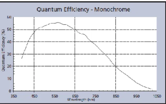
Fig. 1: Quantum Efficiency versus wavelength for MT9M001 CMOS area image sensor (Micron Technology, 2004).
Fig. 2: Lighting System.
1- CMOS Image Sensor, MT9M001:
(a) (b)
Fig. 3: MT9M001 CMOS area image sensor (a) rear view (b) front view.
CMOS area image sensor, MT9M001 is a product from Aptina. It consists of 1.3 Megapixels with 1028x1024 active pixels. Each pixel has a dimension of 5.2 µm x 5.2 µm. It is low power device which operates at 3 ± 0.3 volts. The CMOS area image sensor is chosen instead of commercial digital camera for the tomography system because it is much easier to acquire direct access to each of the pixel value (Philippson, 2007).
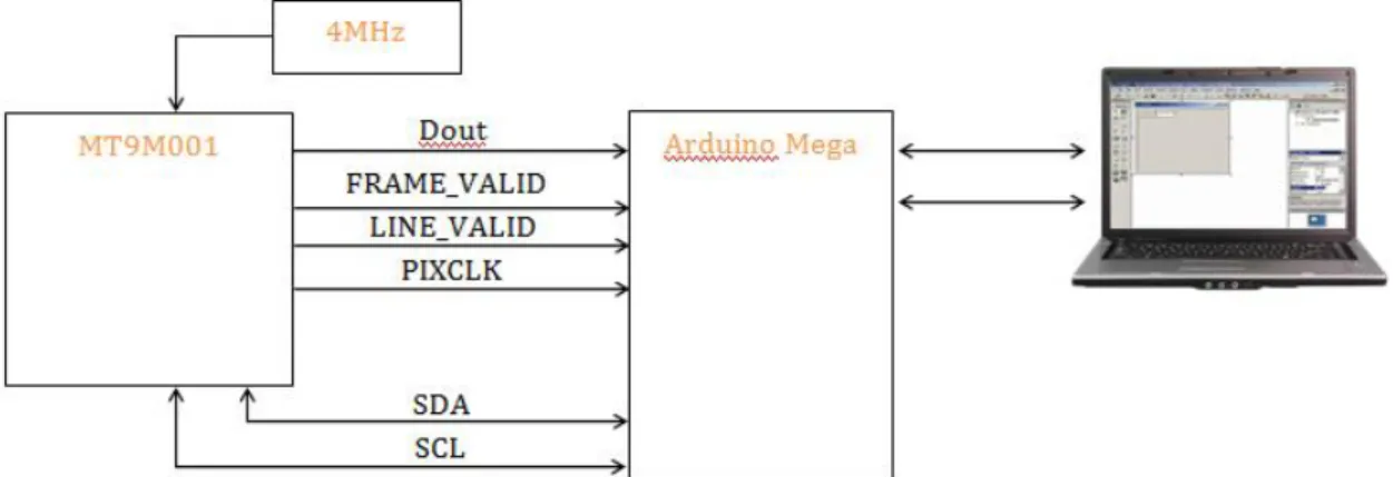
2- Control Circuit and synchronization signals:
The hardware for this project is straight-forward. It consists of Arduino Mega 2560 as the main processor
and CMOS area image sensor as an optical sensor (Error! Reference source not found.). Arduino Mega 2560
Fig. 4: DAQ block diagram.
Table 1: MT9M001 Register setting.
Register Description Default value Chosen Value
0x01 Row Start 0x000C 0x000C
0x02 Column Start 0x0014 0x0014
0x03 Row Size (Window Height) 0x03FF 0x0050
0x04 Column Size (Window Width) 0x04FF 0x0050
Fig. 4: Flowchart to read data from image sensor.
The image sensor runs at 4MHz and output its pixel data when the FRAME_VALID and LINE_VALID signals are high. The Dout are sent to the Arduino Mega at the rising edge of PIXCLK.
RESULTS AND DISCUSSIONS
The arrangement of lighting system with the respective CMOS area image sensor is shown in
Fig. 5. The Lighting system is positioned opposite to the CMOS area image sensor to ensure that the laser light
is well-collimated and strikes the image sensor accurately.
Fig. 5: The arrangement of one projection.
The active surface of the CMOS area image sensor faced the obstacle inside the process vessel. For the purpose of testing, 80x80 pixels from the entire effective pixel is used, which is from (12,20) until (92,100) to represent (row, column). To verify the functionality of the CMOS image sensor, seven (7) conditions were tested:
i. Fully exposed
ii. Fully blocked
iii. Partially right blocked
iv. Partially left blocked
v. Partially upper blocked
vi. Partially lower blocked
vii. Wire shape blocked
The output from the CMOS area image sensor is in term of digital value which represents the light energy falling at the corresponding pixel. For the 8 bit data output, a value 0 will represent white and 255 will denote as black, and the values in between are shades in grey.
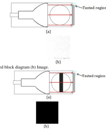
Fig. 8: (a) Fully blocked block diagram (b) Image
Error! Reference source not found.(a) and Error! Reference source not found.(a) indicate the arrangement to test the pixel area when it is fully exposed to the light and fully closed by the obstacle,
respectively. A blue box is a pixel area that is being tested. Error! Reference source not found.(b) is the image
captured when the image sensor is free from any obstacle, and Error! Reference source not found.(b) shows
when the image sensor is fully blocked. Visual Basic 6.0 is used as a medium to display the image that is being captured by the CMOS area image sensor.
Fig. 10: (a) Partially right blocked block diagram (b) Image.
Fig. 9: (a) Partially left blocked block diagram (b) Image.
The image captured by the image sensor when it is being obstructed at the right (Error! Reference source
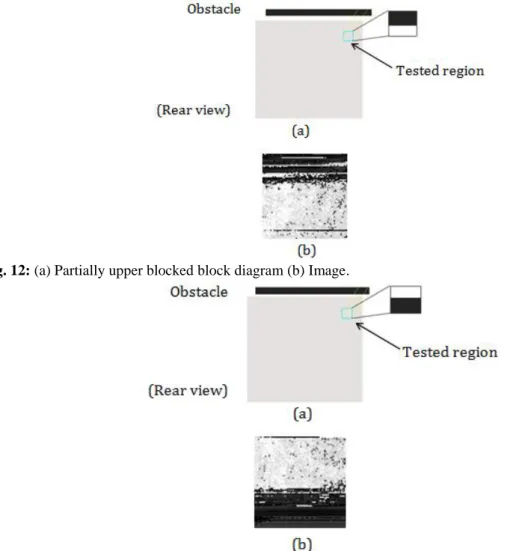
Fig. 12: (a) Partially upper blocked block diagram (b) Image.
Fig. 11: (a) Partially lower blocked block diagram (b) Image.
Error! Reference source not found. (b) and Error! Reference source not found. (b) displayed the image from VB 6.0 to indicate the image that has been snapped when the tested pixel area is partially blocked at upper
region (Error! Reference source not found.(a)) and lower region (Error! Reference source not found. (a)).
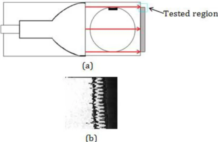
Fig. 13: (a) Closed by wire shape block diagram (b) Image.
A wire has been placed in front of the CMOS image sensor (Error! Reference source not found.(a)). Only
half of the object is included in the test area due to the size of the object is bigger than the test region. The image
shows by VB 6.0 (Error! Reference source not found.(b)) indicates that the image sensor is successfully
captured the shadow of the wire that is positioned in front of it.
Conclusion:
developed optical tomography system is low cost and easy to be integrated to the microcontroller to produce its own DAQ.
ACKNOWLEDGMENTS
The authors would like to acknowledge the Malaysian Ministry of Education and Universiti Teknikal Malaysia Melaka for their support give.
REFERENCES
Bigas, M., E. Cabruja, J. Forest, J. Salvi, 2006. Review of CMOS image sensors. Microelectronics Journal, 37(5): 433–451. doi:10.1016/j.mejo.2005.07.002
Dickin, F.J., R.C. Waterfall, R.A. Williams, CG. Xie, MS. Beck, SM. Huang, C. Lenn, 1992. Tomographic imaging of industrial process equipment: techniques and applications. IEE Proceedings G Circuits, Devices and Systems, 139(1): 72.
Ibrahim, S., R.G. Green, K. Dutton, R.A. Rahim, 2000Application of optical tomography in industrial
process control system. 2000 TENCON Proceedings. Intelligent Systems and Technologies for the New
Millennium (Cat. No.00CH37119), 1: 493–498.
Idroas, M., R. Abdul Rahim, M.H.F. Rahiman, RG. Green, M.N. Ibrahim, 2010. Optical Tomography System: Charge-coupled Device Linear Image Sensors. Sensors & Transducers Journal, 120(9): 62–69.
Micron Technology, I., 2004. 1 / 2-Inch Megapixel CMOS Digital Image Sensor, pp: 1–35.
Philippson, J., 2007. Development of Optoelectronic Devices and Computational Tools for the Production
and Manipulation of Heavy. Queen’s University.
Rahim, R.A., K.S. Chan, J.F. Pang, L.C. Leong, 2005. A hardware development for optical tomography
system using switch mode fan beam projection. Sensors and Actuators A: Physical, 120(1): 277–290.
doi:10.1016/j.sna.2004.11.038
Rahim, R.H.A., 2004. Optical tomography system for process measurement using light-emitting diodes as a light source. Optical Engineering, 43(5): 1251.
Schleicher, E., M.J. da Silva, S. Thiele, A. Li, E. Wollrab, U. Hampel, 2008. Design of an optical
tomograph for the investigation of single- and two-phase pipe flows. Measurement Science and Technology,