© 2015, IRJET.NET- All Rights Reserved
Page 555
A Review of Modulation Techniques for Chopper cell based Modular
Multilevel Converters
Gayathri G
1, Rajitha A R
21
P G Student, Electrical and Electronics, ASIET Kalady, Kerala,India
2Assistant professor, Electrical and Electronics, ASIET Kalady, Kerala,India
---***---Abstract -
Modular multilevel converters (MMCs) arean emerging converter topology with advantages of scalability, modularity, reliability, and efficiency making high voltage and power capability possible. They are becoming a more common converter type because of the increased utilization of High Voltage Direct current (HVDC) power transmission. Its
applications include Railway electric traction
systems(for supplying traction motors), interfacing renewable energy power sources to the grid and motor drives etc. MMCs are beneficial for medium voltage motor drives because of its properties such as low distortion, which allows for an efficient motor drive design. The chopper cell configuration (Half bridge cell) is the simplest submodule configuration of MMC. The converter is made up of a series of IGBT half-bridge circuits with a capacitor across both devices. In this paper different modulation techniques using single reference, two reference and multiple reference used for chopper cell based MMC are reviewed.
Key Words:
Modular multilevel converter, Modulation
techniques, Chopper cell configuration,
High Voltage
Direct current (HVDC).
1. INTRODUCTION
High Voltage DC transmission system using voltage-source converters provides a means of connecting distant renewable sources to a large ac power network [1],[2].Conventional VSC based HVDC systems usually use two-level or three-level converters which has disadvantages like uneven voltage distribution across each IGBT, low power quality and high switching loss. Modular multilevel converters (MMCs) can be easily implemented for obtaining high number of levels. It uses more commercially available low-rated IGBTs, so the semiconductor device cost is reduced and also reduced use of filter components. Modular design, excellent output
voltage waveforms, low switching frequency, high efficiency are the advantages of MMC [3]-[5].
Multilevel converters have great demand in the electrical power industry in recent years. They have a lot of advantages that makes them suited for high voltage systems and power system applications .Its special structure makes them to work at a very high voltage with low harmonic content. For ac/dc and dc/ac conversion, which is a major requirement in high-voltage high-power applications, the Diode clamped converter topology is used [6]-[8].But, the proper use of this topology requires balancing of the dc link capacitor voltages. A two switch based MMC proposed in [9] is simpler than the cascaded 4-switch H-bridge-based converter and has advantages like modular extension to any number of levels and simplicity.
The principle of operation of the modular multilevel inverters is discussed in [9],[10].Space vector modulation with the modular multilevel converter is vague, because the converter depends on phase voltage redundancy in balancing the capacitor voltages rather than line-to-line voltage as in case of the diode-clamped inverter. Classification of modular multilevel converters, capacitor voltage balancing methods and its control systems have been discussed in [11].Reference [9] explains the importance of capacitor voltage balancing. The explanations of the necessary capacitor voltage balancing methods are discussed in [12]-[18].
2. CIRCUIT CONFIGURATION AND WORKING OF
MMCs
© 2015, IRJET.NET- All Rights Reserved
Page 556
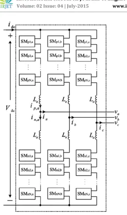
Fig -1: Schematic representation of DSCC-MMCThe structure of MMC is well explained in references [19],[20],[21].Suffixes p and n denotes the upper and the lower arms respectively of the three phases a, b and c. Lo represents the series inductor. Idc and Vdc are the dc link voltage and current respectively. The ac currents through the three phases are ia, ib and ic.Fig.2 shows the capacitor across the two devices is either directly connected into the converter or shorted out depending on the state of the driving gate signals. Some other properties of the converter topology are that this sequence of sub modules along with an arm inductor makes an arm of the converter as shown in Fig.1.The two arms make up one phase of the converter, known as a phase unit. The center point between the arm inductors are connected to the AC side while the phase units are connected in parallel to the DC bus. Every submodule acts as independent DC voltage sources. The number of sub modules chosen is based on the power levels and applications that will be utilized. A typical minimum number of levels is a 5-level MMC which has four submodules per arm. If the number of
submodules is equal to N, the modular multilevel converter is described as a (N+1) level MMC. This is because 0 volts is included as a voltage level.
Fig -2: Chopper cell submodule
3. MODULATION TECHNIQUES
[image:2.595.38.298.59.498.2]Conventional pulse width modulation (PWM) uses one reference waveform and one carrier waveform to generate a gate driving signal. The reference is compared to the carrier and if the carrier is lower than the reference, the PWM output is high and if the carrier is higher than the reference then the PWM output is low. Considering the three phase half bridge circuit discussed above, this pulse width modulation technique can be used to control a conventional voltage source converter. The PWM signal controls the top switch in the half bridge circuit while the inverse of this signal controls the bottom switch in the circuit. For modular multilevel converters, it has several of these half-bridge circuits in the converter that all need to be individually controlled. Thus the solution to this issue is to use multicarrier PWM methods. A carrier waveform is required for each half-bridge circuit, or submodule, in the converter.
Fig-3: PWM techniques based on carriers
[image:2.595.333.534.515.658.2]© 2015, IRJET.NET- All Rights Reserved
Page 557
Fig-4: PWM techniques based on reference waveformPWM techniques based on single reference waveform include:
1) Carrier Disposition PWM (CD-PWM) technique [22],[23]:It requires N triangular carriers which are identical and are equally displaced with respect to zero axis. This carriers are compared with the reference waveform to produce the desired switched output phase voltage level.The Voltage variations corresponding to a triangular carrier are associated with the insertion or bypass of a particular submodule. Based on the phase shift among the carrier waveforms, these techniques are further classified into: PD (phase disposition),POD (phase opposition disposition), and APOD (alternate phase opposition disposition).But its drawbacks include unequal distribution of voltage ripple across the SM capacitors that impact the harmonic distortion of the ac side voltages and large magnitudes of circulating currents. To mitigate the harmonic problems of the ac-side voltages, simple carrier rotation technique [24], modified carrier rotation technique [25], or signal rotation technique [22] is used to make the voltage distribution across all the SM capacitors equal. Its output voltages may have a relatively high total harmonic distortion (THD). For improving the performance of these techniques, a modified PD PWM technique with a SM capacitor voltage balancing technique is proposed in [12].In this method, voltage variations corresponding to a triangular carrier are no longer assigned to a particular submodule.
In this technique, comparison of the reference waveform with the carrier waveforms produces an (N + 1)-level waveform which determines the number of SMs to be inserted in theupper and arms, respectively. The determined number of SMs out of the N submodules in the upper or lower arm are inserted depending upon the direction of the arm current and the status of the SM capacitor voltages, in order to minimize the difference between the SM capacitor voltages. In reference [26] a PD PWM technique with selective loop bias mapping method for balancing the submodule capacitors. This method implements carrier rotation using the feedback of the maximum or minimum SM capacitor voltages and the direction of arm current.
2) Subharmonic techniques: 2N identical carriers are used in this technique and can be either sawtooth or triangular.Each carriers are phase shifted by 360⁰/N [22].
The PWM techniques which make use of two reference waveforms are:
1) Direct modulation technique: In this technique voltages of both the arms of phase a is controlled by using two complementary sinusoidal reference waveforms and it is given by equation
(1)
(2)
The reference waveforms in (1) and (2) are compared with the PD carrier waveforms, which vary between 0 and N, to determine the required number of inserted SMs in the upper and lower arms.
2) Indirect modulation technique: Here the upper and lower arm reference waveform of phase a is given by,
(3)
(4)
where where Vcx,I,a represents the capacitor
© 2015, IRJET.NET- All Rights Reserved
Page 558
with the PD carrier waveforms to determine thenumber of inserted SMs in the upper and lower arms. This technique can be further classified into closed loop control and open loop control.
3) Phase shifted carrier PWM (PSC-PWM):In this technique, each SM of the MMC is controlled independently, and the voltage balancing task of the SMs is divided into an averaging control and a balancing control. The reference waveforms of each SM in the upper and lower arms are given by
(5)
(6)
Here is the averaging controller output and is the individual balancing controller output. The averaging and balancing techniques control the average SM capacitor voltage in each phase-leg and the individual SM capacitor voltage, respectively. Comparison of each SM voltage reference waveform with its triangular carrier generates the switching signals for the corresponding SM. The triangular carrier waveforms of each phase-leg are implemented based on the sub harmonic techniques. The main drawbacks of this technique are its implementation effort that significantly increases as the number of SMs increases and instability under certain operating conditions [20],[27].
4. SIMULATION AND REUSLTS
Fig.5 shows the Simulink model of a single phase three level MMC. Modulation techniques based on single reference waveform was developed and compared. Line to line voltage total harmonic distortion for three carrier disposition strategies was compared and the results were tabulated. Parameters are given below.
Parameters Specification
DC supply voltage 140V
DC capacitance 3mF
Buffer inductance 1mH
Rated frequency 50Hz
Carrier frequency 1KHz
Load inductance 0.1mH
Fig-5 : Simulation diagram of MMC
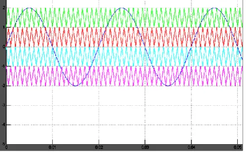
This paper discusses the comparison of In phase disposition, phase opposition disposition and alternate phase opposition disposition strategies and their effect on line to line THD. The simulation for a 5-level MMC requires 4 carriers and a single sinusoidal reference waveform.Fig.6 shows In phase disposition PWM strategy where all carriers are in phase.
Fig-6 : In phase disposition PWM
© 2015, IRJET.NET- All Rights Reserved
Page 559
alternate phase disposition method, all the adjacent [image:5.595.37.289.141.297.2]carriers are phase shifted by 180 degrees. It is shown in Fig.8.
Fig-7 : Phase opposition disposition method
Fig-8 : Alternate phase opposition disposition method
The table shows the comparison of line to line voltage THD of the MMC with the above said modulation strategies.
Table -1: Comparison of modulation strategies
Modulation methods
Vab Vbc Vca
PD 17.37% 17.12% 16.91%
POD 22.25% 17.12% 22.30%
APOD 25.29% 26.02% 25.35%
5. CONCLUSIONS
In this paper different modulation strategies used for chopper cell based Modular multilevel converter was discussed. Modulation techniques based on single reference waveform was analyzed separately on the basis on line to line total harmonic distortion. From eliminating harmonics point of view, the In phase disposition method was found to be the best and alternate phase disposition method is the worst.
REFERENCES
[1] K. Friedrich, “Modern HVDC PLUS application of VSC in modular multilevel converter topology,” in Proc. Int. Symp. Ind. Electron., 2010,pp. 3807–3810.
[2] P. Bresesti, W. L. Kling, R. L. Hendriks, and R. Vailati, “HVDC connection of offshore wind farms to the transmission system,” IEEE Trans.Energy Convers., vol. 22, no. 1, pp. 37–43, Mar. 2007.
[3] A. Lesnicar and R. Marquardt, “An innovative modular multilevel converter topology suitable for a wide power range,” in Proc. IEEE Power Tech Conf., 2003, vol. 3, pp. 23–26.
[4] R. Marquardt, “Modular multilevel converter: An universal concept for HVDC-networks and extended DC-bus-applications,” in Proc. IEEE Power Electron. Conf., 2010, pp. 502–507.
[5] S. Rohner, S. Bernet, M. Hiller, and R. Sommer, “Modulation, losses and semiconductor requirements of modular multilevel converters,” IEEE Trans. Ind. Electron., vol. 57, no. 8, pp. 2633–2642, Aug. 2010. [6] POU J., PINDADO R., BOROYEVICH D.: “Voltage
balance limits infour level diode clamped converter with passive front ends”,IEEE Trans. Ind. Electron., 2005, 52, (1), pp. 190–196
[7] SAEEDIFARD M., NIKKHAJOEI H., IRAVANI R.: “A space vector modulated STATCOM based on a three-level neutral point clamped converter”, IEEE Trans. Power Deliv., 2007, 22,(2), pp. 1029–1039
[8] NEWTON C., SUMNER M.: “Novel technique for maintaining balanced internal DC link voltages in diode clamped fivelevel inverters”, IEEE Proc. Electr. Power Appl., 1999, 146, (3), pp. 341–349
[9] LESNICAR A., MARQUARDT R.: “An innovative modular multilevel converter topology suitable for a wide power range”. IEEE PowerTech Conf., Bologna, Italy, 23–26 June 2003, vol. 3
[10]GLINKA M., “Prototype of multiphase modular multilevel-converter with 2 MW power rating and 17-level-output-voltage”. IEEE 35th Annual Power Electronics Specialists Conf., vol. 4, issue 2004, pp. 2572–2576
[image:5.595.37.290.340.494.2]© 2015, IRJET.NET- All Rights Reserved
Page 560
Electronic Specialist Conf., 15–19 June 2008, pp. 154–161
[12]M. Saeedifard and R. Iravani, “Dynamic performance of a modular multilevel back-to-back HVDC system,” IEEE Trans. Power Del., vol. 25,no. 4, pp. 2903–2912, Oct. 2010.
[13]J. Qin and M. Saeedifard, “Predictive control of a modular multilevel converter for a back-to-back HVDC system,” IEEE Trans. Power Del., vol. 27, no. 3, pp. 1538–1547, Jul. 2012.
[14]M. Hagiwara and H. Akagi, “Control and experiment of pulse width modulated modular multilevel converters,” IEEE Trans. Power Electron.,vol. 24, no. 7, pp. 1737–1746, Jul. 2009.
[15] F. Deng and Z. Chen, “A control method for voltage balancing in modular multilevel converters,” IEEE Trans. Power Electron., vol. 29, no. 1,pp. 66–76, Jan. 2014.
[16]S. Rohner, S. Bernet, M. Hiller, and R. Sommer, “Modelling, simulation and analysis of a modular multilevel converter for medium voltage applications,” in Proc. IEEE Int. Conf. Ind. Technol., 2010, pp. 775–782.
[17]M. Dommaschk, J. Dorn, I. Euler, J. Lang, Q.-B. Tu, and K. Wrflinger,“Drive of a phase module branch of a multilevel converter,” in U.S. Patent US2010/0060235A1, Mar. 11, 2010.
[18]S. Rohner, S. Bernet, M. Hiller, and R. Sommer, “Modulation, losses,and semiconductor requirements of modular multilevel converters,”IEEE Trans. Ind. Electron., vol. 57, no. 8, pp. 2633–2642, Aug.2010. [19]Suman Debnath ,JiangchaoQin, Behrooz Bahrani,
Maryam Saeedifard, and Peter Barbosa, “Operation, Control, and Applications of the Modular Multilevel Converter”, IEEE TRANSACTIONS ON POWER ELECTRONICS, VOL. 30, NO. 1, JANUARY 2015. [20]N. Thitichaiworakorn, M. Hagiwara, and H. Akagi,
“Experimental verification of a modular multilevel cascade inverter based on double-star bridge-cells (MMCI–DSBC),” IEEE Trans. Ind. Appl., vol. PP, no. 99,pp. 1–1, Jan. 2013.
[21]H. Akagi, “New trends in medium-voltage power converters and motor drives,” in Proc. IEEE Int. Symp. Ind. Electron., 2011, pp. 5–14.
[22]G. Konstantinou and V. Agelidis, “Performance evaluation of half-bridge cascaded multilevel converters operated with multicarrier sinusoidal PWM techniques,” in Proc. IEEE Conf. Ind. Electron. Appl., 2009, pp. 3399–3404
[23]A. Hassanpoor, S. Norrga, H. Nee, and L. Angquist, “Evaluation of different carrier-based PWM methods for modular multilevel converters for HVDC application,” in Proc. Conf. IEEE Ind. Electron. Soc., 2012, pp. 388–393.
[24]D.-W. Kang, W.-K. Lee, and D.-S. Hyun, “Carrier-Rotation strategy for voltage balancing in flying
capacitor multilevel inverter,” IEE Proc.Electric Power Appl., vol. 151, no. 2, pp. 239–248, 2004.
[25] B.-S. Jin, W. kyo Lee, T.-J. Kim, D.-W. Kang, and D.-S. Hyun, “A study on the multi-carrier PWM methods for voltage balancing of flying capacitor in the flying capacitormulti-level inverter,” in Proc. Conf. IEEE Ind. Electron. Soc., 2005, p. 6.
[26]J. Mei, K. Shen, B. Xiao, L. Tolbert, and J. Zheng, “A new selective loop bias mapping phase disposition PWM with dynamic voltage balance capability for modular multilevel converter,” IEEE Trans. Ind. Electron.,vol. 61, no. 2, pp. 798–807, Feb. 2014.
[27]M. Hagiwara, R. Maeda, and H. Akagi, “Control and analysis of the modular multilevel cascade converter based on double-star chopper-cells (MMCC–DSCC),” IEEE Trans.Power Electron., vol. 26, no. 6, pp. 1649– 1658, Jun. 2011.
BIOGRAPHIES
Gayathri G was born in Kerala, India in 1990. She received the Bachelor of Technology degree in Electrical and Electronics from Saintgits College of Engineering and Technology, Kottayam in 2013. She is currently pursuing Master of Technology in Power Electronics and Power System at Adi Shankara Institute of Engineering and Technology, Cochin. Her current research interests include HVDC systems, and Multilevel converters.