© 2016, IRJET | Impact Factor value: 4.45 | ISO 9001:2008 Certified Journal
| Page 1956
AC, DC, Transient and FFT Analysis of Multistage Operational
Amplifiers using 0.3µm process technology for CMOS
Anju Sharma
1, Brahmi Shrman
21,2
Department of Electronics and Communication Engineering
NRI Institute of Science and Technology Raisen Road, Bhopal India
1
[email protected]
2[email protected]
---***---Abstract -
In this paper, a fully differential CMOS operational amplifier was designed using a 0.3µm library process. The supply voltage is a 1.8 V or 3.2 V source with variation depends on the analysis done. The op-amp was specified to meet several specifications over process variations that include slow-slow, slow-fast, fast-slow, and fast-fast for PMOS and NMOS transistors. A folded cascade stage with CMOS driven common source amplifier output stage was used that met all the specifications except for the settling time. Process corner simulations showed a dramatic decrease in performance,. This paper discusses the design approach, frequency response and time domain simulation results, rejection ratio performance for common mode and power supply, and closes with a retrospective look at lessons learned and ways to improve the operational amplifier design. This paper also discuss design methodologies and frequency analysis of two stage and three stage. Response curves are plotted for AC characteristics of different topologies of multistage operational amplifiers are tabulated for suitable frequency ranges. Transients are also plotted from nanoseconds scale to microseconds scale. Subsequently FFTs are also tabulated at frequency range from 1 MHz to 25 GHz. By results and reasons in this paper two stage and three stage topologies are suitable choices for low voltage and high performance applications.Key Words: Operational Amplifiers, CMOS, FFT, Process technology, Amplifiers, MOS transients
1.INTRODUCTION
Operational Amplifiers are one of the most widely used building blocks for analog and mixed-signal systems. They are employed from dc bias applications to high speed amplifiers and filters. General purpose op amps can be used as buffers, summers, integrators, differentiators, comparators, negative impedance converters, and many other applications. With the quick improvements of computer aided design (CAD) tools, advancements of semiconductor modelling, steady miniaturization of transistor scaling, and the progress of fabrication processes, the integrated circuit market is growing rapidly. Nowadays, complementary metal-oxide semiconductor (CMOS) technology has become dominant over bipolar technology for analog circuit design in amixed-signal system due to the
industry trend of applying standard process technologies to implement both analog circuits and digital circuits on the same chip. While many digital circuits can be adapted to a smaller device level with a smaller power supply, most existing analog circuitry requires considerable change or even a redesign to accomplish the same feat. With transistor length being scaled down to a few tens of nanometers, analog circuitsare becoming increasingly more difficult to improveupon. The classic Widlar op amp architecture, originally developed for bipolar devices [10], has required modification for use with CMOS devices. In particular, it has proved difficult to match the open loop gain of bipolar op amps with CMOS technology [3, 4]. This is due to the inherently lower trans-conductance of CMOS devices aswell as the gain reduction due to short channel effects thatcome into play for submicron CMOS processes.
2.
A
MPLIFIERSOperational amplifiers typically are composed of either two or three stages consisting of a differential amplifier, a gain stage and an output stage as seen in Figure 1. In some applications, the gain stage and the output stage are one and the same if the load is purely capacitive. However, if the output is to drive a resistive load or a large resistive load, then a high current gain buffer amplifier is used at the output. Each stage plays an important role in the performance of the amplifier.
© 2016, IRJET | Impact Factor value: 4.45 | ISO 9001:2008 Certified Journal
| Page 1957
The differential amplifier offers a variety of advantages and is always used as the input to the overall amplifier. Since it provides common-mode rejection, it eliminates noise common on both inputs, while at the same time amplifying any differences between the inputs.The limit for which this common mode rejection occurs is called common-mode range and signifies the upper and lower common modesignal values for which the devices in the diff-amp are saturated. The differential amplifier also provides gain.
The gain stage is typically a common-source or cascade type amplifier. So that the amplifier is stable, a compensation network is used to intentionally lower the gain at higher frequencies. The output stage provides high current driving capability for either driving large capacitive or resistive loads.
Fig.2. Block Diagram of a generic amplifier
The outputstage typically will have low output impedance and high signal swing characteristics. In some cases, itmay be advantageous to add bipolar devices to improve the performance of the circuitry. These will bepresented as the multi stage opamp circuits are analysed.
3.TWO-STAGE
CMOS
OPERATIONAL
AMPLIFIER
Operational Amplifiers are the backbone for many analog circuit designs. Operational amplifiers are one of the basic and important circuits which have a wide application in several analog circuits such as switched capacitor filters, algorithmic, pipelined and sigma delta A/D converter, sample and hold amplifier etc. The speed and accuracy of these circuits depends on the bandwidth and DC gain of the operational amplifiers. Larger the bandwidth and gain, higher the speed and accuracy of the operational amplifier are a critical element in analog sampled data circuit, such as SC filters, modulators [4]. The first block is a differential amplifier. It has two inputs which are the inverting and non-inverting voltage. It provides at the output a differential voltage or a differential current that, essentially, depends on the differential input only. The next block is a differential to single-ended converter. It is used to transform the differential signal generated by the first block into a single ended version. Some architecture doesn’t require the differential to single ended function; therefore the block can be excluded. In most cases the gain provided by the input
stages is not sufficient and additional amplification is required. This is provided by intermediate stage, which is another differential amplifier, driven by the output of the first stage.As this stage uses differential input unbalanced output differential amplifier, so it provide required extra gain. The bias circuit is provided to establish the proper operating point for each transistor in its saturation region. Finally, we have the output buffer stage. It provides the low output impedance and larger output current needed to drive the load of operational amplifier or improves the slew rate of the operational amplifier. Even the output stage can be dropped: many integrated applications do not need low output impedance; moreover, the slew rate permitted by the gain stage can be sufficient for the application. If the operational amplifier is intended to drive a small purely capacitive load, which is the case in many switched capacitor or data conversion applications, the output buffer is not used. When the output stage is not used the circuit, it is an operational trans-conductance amplifier, OTA. The purpose of the compensation circuit is lower the gain at high frequencies and to maintain stability when negative feedback is applied to the operational amplifier [7].
Fig.3 Schematic for topology 1 for two stage Operational amplifier
© 2016, IRJET | Impact Factor value: 4.45 | ISO 9001:2008 Certified Journal
| Page 1958
4.THREE-STAGE
CMOS
OPERATIONAL
AMPLEFIER
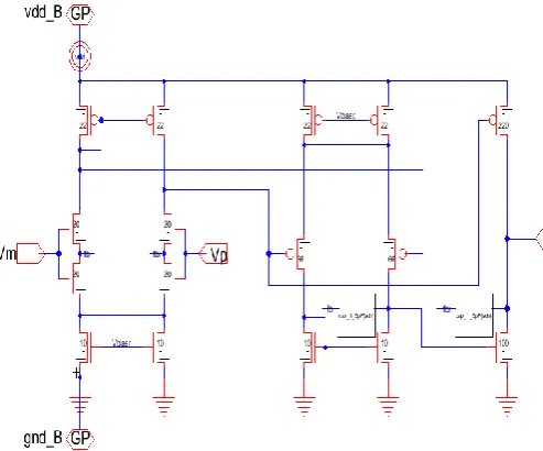
[image:3.595.380.483.105.275.2]Three stage operational amplifiers are used in applications where low power is required or that can operate with low supply voltage or with minimal power from VDD. In comparison to two –stage operational amplifiers the bias circuit is to be developed can pull more current from VDD than the operational amplifiers it biases. So I have used two circuit architectures for biasing circuits. For proper operation of the output stage floating current sources are generally preferred. Towards keeping a large gain and lowering the power supply voltage, considering the three stage operational amplifier above. The design is cascade of two different differential amplifier stages followed by a common source amplifier. If we connect a resistive load to the output of the common source stage, the overall operational amplifier gain remains relatively high due to the cascaded gain of two differential amplifier stages. This topology of operational amplifier i.e. more than two stages is a sort of compensation. The compensation of capacitors within the operational amplifier for overall improvement in the desired operational amplifier characteristics[3,6].
Fig.5 Schematic for topology 3, two stage operational amplifier
[image:3.595.326.540.308.465.2]5. Design Methodology And Design Flow
It is assumed that all transistors are in saturation for the above relationships. The design in this project is a two-stage op amp with an n-channel input pair. The op amp uses a dual-polarity power supply (Vdd and Vss) so the ac signals can swing above and below ground and also be centered at ground.[38] Design flow approach regarding the same is as followsFig.6. Design Flow used for OpAmp Design
Fig.7. Design Procedure
[image:3.595.39.286.409.614.2]6.Simulation Results and FFT Plots
Fig. 8 Simulation plot for DC analysis of 2 stage
Operational Amplifier (V
(out)and d(V
(out))
Circuit Requirements
and Specifications
Determine Circuit Parameters
Initial Circuit
Simulate Circuit
Select Circuit Topology
Topology
Selected Modified Circuit
Parameters
Change Circuit Parameters
Teste d OK
Current mirrors and Biasing Networking
Design
Differential Input Stage Amplifier
Design
Control Network / Output Stage
[image:3.595.312.559.506.726.2]© 2016, IRJET | Impact Factor value: 4.45 | ISO 9001:2008 Certified Journal
| Page 1959
Fig.9 AC Analysis plot for Voutin 2 stage Operational
Amplifier
Fig.10 Transient Analysis plot for V
outin 2 stage
Operational Amplifier
Fig.11 AC Analysis plot for V
outin 2 stage Operational
Amplifier
Fig.12Transient analysis plot for V
outand V
inin
multistage operational amplifier topology
Fig.13 Transient analysis for multistage
operational amplifier topology2 with capacitive load
© 2016, IRJET | Impact Factor value: 4.45 | ISO 9001:2008 Certified Journal
| Page 1960
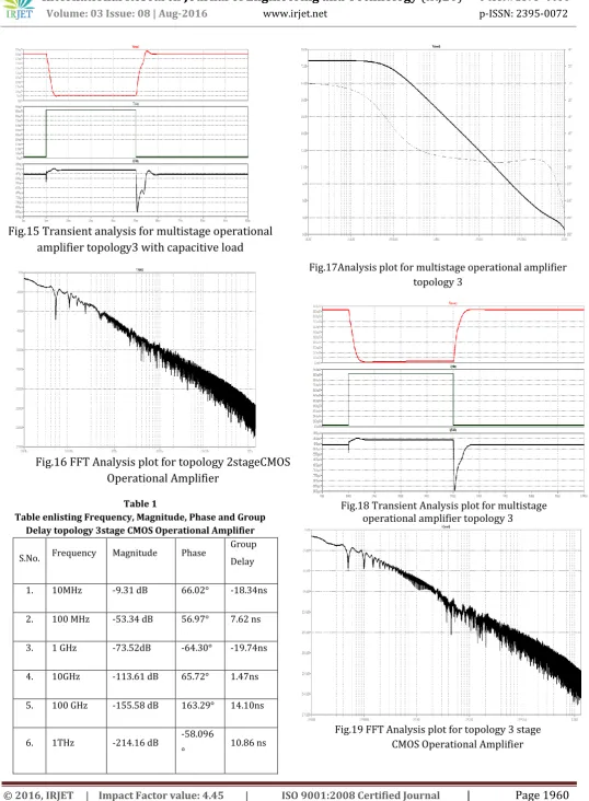
Fig.15 Transient analysis for multistage operational
amplifier topology3 with capacitive load
[image:5.595.299.560.57.283.2]Fig.16 FFT Analysis plot for topology 2stageCMOS
Operational Amplifier
Table 1
Table enlisting Frequency, Magnitude, Phase and Group Delay topology 3stage CMOS Operational Amplifier
S.No. Frequency Magnitude Phase
Group Delay
1. 10MHz -9.31 dB 66.02° -18.34ns
2. 100 MHz -53.34 dB 56.97° 7.62 ns
3. 1 GHz -73.52dB -64.30° -19.74ns
4. 10GHz -113.61 dB 65.72° 1.47ns
5. 100 GHz -155.58 dB 163.29° 14.10ns
6. 1THz -214.16 dB -58.096
[image:5.595.33.572.59.792.2]° 10.86 ns
Fig.17Analysis plot for multistage operational amplifier topology 3
Fig.18 Transient Analysis plot for multistage operational amplifier topology 3
[image:5.595.45.271.301.478.2]© 2016, IRJET | Impact Factor value: 4.45 | ISO 9001:2008 Certified Journal
| Page 1961
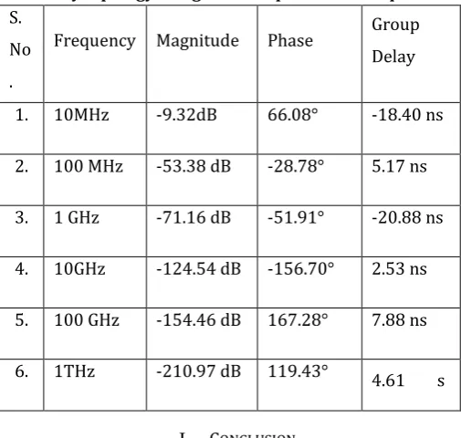
[image:6.595.31.284.135.375.2]Table 2
Table enlisting Frequency, Magnitude, Phase and Group Delay topology 4stage CMOS Operational Amplifier
S. No .
Frequency Magnitude Phase Group
Delay
1. 10MHz -9.32dB 66.08° -18.40 ns
2. 100 MHz -53.38 dB -28.78° 5.17 ns
3. 1 GHz -71.16 dB -51.91° -20.88 ns
4. 10GHz -124.54 dB -156.70° 2.53 ns
5. 100 GHz -154.46 dB 167.28° 7.88 ns
6. 1THz -210.97 dB 119.43° 4.61 s
I. .CONCLUSION
Keeping in view different applications the Op-amp has been designed. For this first a selection is made for the active device used. Different topologies of multistage operational amplifiers are analyzed for various transients and FFT responses are calculated for frequencies ranging from 1MHz to 25 MHz AC analysis. The development of a design procedure provides a quick, well integrated and effective mechanism for estimation and calculation of various parameters. The steps highlighted make it easy to redesign the circuit for various set of specifications. The responses are simulated using LTSpice and Electric VLSI CAD design tool. The simulated results of the Op-amp are in compliance with the theoretical values.
REFERENCES
[1] Dr.Soni Changlani, Ayoush Johari “Implementation , analysis and comparison of 2 stage and 3 stage and multistage Operational Amplifiers” CICN IEEE Conference November 2014
[2] Perenzoni, Matteo, Luca Parmesan, and David Stoppa. "A robust, power-and area-efficient gm-control for low-noise operational amplifiers." Analog Integrated Circuits and Signal Processing 82.1 (2015): 209-216. [3] Grassi, Marco, Jean-Michel Redoute, and Anna Richelli.
"Increased EMI immunity in CMOS operational amplifiers using an integrated common-mode cancellation circuit." Electromagnetic Compatibility (EMC), 2015 IEEE International Symposium on. IEEE, 2015.
[4] Tepwimonpetkun, Samattachai, BhirawichPholpoke, and WoradornWattanapanitch. "Graphical analysis and design of multistage operational amplifiers with active
feedback Miller compensation." International Journal of Circuit Theory and Applications (2015).
[5] Ohno, Yasuhiko, et al. "Maximum and minimum voltage sample and hold circuits employing operational amplifiers composed of polycrystalline silicon thin-film transistors." Future of Electron Devices, Kansai (IMFEDK), 2014 IEEE International Meeting for. IEEE, 2014.
[6] Vigraham, Baradwaj, JayanthKuppambatti, and Peter R. Kinget. "Switched-Mode Operational Amplifiers and Their Application to Continuous-Time Filters in Nanoscale CMOS." Solid-State Circuits, IEEE Journal of 49.12 (2014): 2758-2772.
[7] Irom, Farokh, Shri G. Agarwal, and MehranAmrbar. "Compendium of Single-Event Latchup and Total Ionizing Dose Test Results of Commercial and Radiation Tolerant Operational Amplifiers." Radiation Effects Data Workshop (REDW), 2014 IEEE. IEEE, 2014. [8] Eschauzier, Rudy GH, and Johan Huijsing. Frequency
compensation techniques for low-power operational amplifiers. Vol. 313. Springer Science & Business Media, 2013.
[9] Ahuja, Bhupendra K. "An improved frequency compensation technique for CMOS operational amplifiers." Solid-State Circuits, IEEE Journal of 18.6: 629-633.
[10]Azmi, Nilofar, and D. Sunil Suresh. "DESIGN OF LOW POWER OPERATIONAL AMPLIFIER USING CMOS TECHNOLOGIES." immunity 2 (2014):
[11]Todani, R. I. S. H. I., and ASHIS KUMAR Mal. "Simulator based device sizing technique for operational amplifiers." WSEAS Trans. Circ. Syst 13.1 (2014): 11-28. [12]Yamatoya, Yuki, Akira Hiroki, and HirokazuOda. "Macromodeling of operational amplifiers for overdrive circuit design." Future of Electron Devices, Kansai (IMFEDK), 2015 IEEE International Meeting for. IEEE, 2015.
[13]Cardoso, Guilherme S., et al. "Reliability Analysis of 0.5 µm CMOS Operational Amplifiers under TID Effects." Journal of Integrated Circuits and Systems 9.1 (2014): 70-79.
[14]Petrov, A. S., K. I. Tapero, and V. N. Ulimov. "Influence of temperature and dose rate on the degradation of BiCMOS operational amplifiers during total ionizing dose testing." Microelectronics Reliability 54.9 (2014): 1745-1748.
[15]Cuong, Nguyen Duy, and Tran Xuan Minh. "Design of analog MRAS controllers using operational amplifiers for motion control systems." Information Science, Electronics and Electrical Engineering (ISEEE), 2014 International Conference on. Vol. 2. IEEE, 2014. [16]Prokopenko, Nikolay N., et al. "The Advanced Circuitry
© 2016, IRJET | Impact Factor value: 4.45 | ISO 9001:2008 Certified Journal
| Page 1962
[17]Jothimurugan, R., et al. "Improved realization of canonical Chua's circuit with synthetic inductor using current feedback operational amplifiers." AEU-International Journal of Electronics and Communications 68.5 (2014): 413-421.
[18]Kusuda, Yoshinori. "5.1 A 60V auto-zero and chopper operational amplifier with 800kHz interleaved clocks and input bias-current trimming." Solid-State Circuits Conference-(ISSCC), 2015 IEEE International. IEEE, 2015.
[19]Bakerenkov, A. S., et al. "Radiation Degradation Modeling of Bipolar Operational Amplifier Input Offset Voltage in LTSpice IV." Applied Mechanics and Materials. Vol. 565. 2014.
[20]Huijsing, Johan, Rudy J. van de Plassche, and Willy Sansen, eds. Analog circuit design: operational amplifiers, analog to digital convertors, analog computer aided design. Springer Science & Business Media, 2013.
[21]Sakurai, Satoshi, and Mohammed Ismail. Low-voltage CMOS operational amplifiers: Theory, Design and Implementation. Vol. 290. Springer Science & Business Media, 2012.
[22]Nakhostin, M., et al. "Use of commercial operational amplifiers in a low cost multi-channel preamplifier system." Radiation Physics and Chemistry 85 (2013): 18-22.
[23]Gray, Paul R., and Robert G. Meyer. "MOS operational amplifier design-a tutorial overview." Solid-State
Circuits, IEEE Journal of 17.6 (1982): 969-982. [24]Lipka, B., and U. Kleine. "Design of a cascoded
operational amplifier with high gain." Mixed Design of Integrated Circuits and Systems, 2007. MIXDES'07. 14th International Conference on. IEEE, 2007.
[25]Baker, R. Jacob. CMOS: circuit design, layout, and simulation. Vol. 18. Wiley-IEEE Press, 2011.
[26]Rao, K. Radhakrishna, and S. Srinivasan. "A band pass filter using the operational amplifier pole." Solid-State Circuits, IEEE Journal of 8.3 (1973): 245-246.