© 2017, IRJET | Impact Factor value: 5.181 | ISO 9001:2008 Certified Journal | Page 544
Design and Implementation of Multiplier using Advanced Booth
Multiplier and Razor Flip Flop
Shubhangi Ramannawar
1, Deepak Kumar
21
M.Tech. Scholar, Department of Electronics & Communication Engineering, Vidhyapeeth Institute of Science &
Technology Bhopal, India (e-mail: [email protected]).
2
Assistant Professor, Department of Electronics & Communication Engineering, Vidhyapeeth Institute of Science &
Technology Bhopal, (RGPV,Bhopal) India (e-mail: [email protected]).
---***---Abstract –
The advancement in digital signal
processing with its various other applications made
digital multipliers to play major role in technology.
Many researchers are working to design multipliers
which offer either of the following design targets – high
speed, low power consumption and less area.
Furthermore, the negative bias temperature instability
effect occurs when a pMOS transistor is under –ve bias
(Vgs = −Vdd), increasing the Vt (threshold voltage) of
the pMOS transistor, and declinement in multiplier
speed. Similarly, +ve bias temperature instability,
occurs when an nMOS transistor is under positive bias.
Both the effects directly hinder the multiplier speed by
degrading transistor speed, if this problem occurs for
long time then the system may fail due to timing
violations.
To overcome the timing violations, Variable
latency technique is used. Therefore, it is important to
design efficient high-performance multipliers.
In this paper, we propose a high speed multiplier
design using Modified booth multiplier algorithm. The
multiplier designed using booth algorithm have two
16-bit input and 32-bit output and is able to provide
higher throughput through the variable latency and can
adjust the AHL circuit with help of Razor flip flop to
mitigate performance degradation that is due to the
aging effect. The design and implementation of
Efficient Multiplier Design using Advanced Booth
Algorithm and Razor Flip Flop. The proposed
architecture is quite different from the Conventional
method of multiplier like row/column bypass
multiplier. The proposed architecture is simulated and
implemented on XilinxISE 14.2
Key Words: NBTI (Negative Bias Temperature
Instability), PBTI (Positive Bias Temperature Instability), Modified Booth Algorithm, Adaptive Hold Logic (AHL), TDDB (Time-Dependent Dielectric Breakdown), BTI (Bias Temperature Instability).
1.
INTRODUCTION
A traditional method to reduce the aging effect is overdesign, including such things as guard-banding and gate over sizing; however, this approach can be very pessimistic and area and power inefficient. For eliminate this problem, number of NBTI-aware methodologies have been proposed. An NBTI-aware technology mapping technique was proposed in to pledge the performance of the circuit during its lifetime. In an NBTI-aware sleep transistor was planned to decrease the aging effects on pMOS sleep-transistors, and the life time stability of the power-gated circuits under consideration was made better. Wu and Marculescu [9] proposed a joint logic restructuring and pin reordering method, which is based on detecting functional symmetries and transistor stacking effects.
No variable-latency multiplier architecture that considers the aging effect and can adapt dynamically has been done. There are many multiplier architectures developed to boost the speed of algebra. Booth algorithm is the most effective algorithm used for faster performances. It is introducing a high performance multiplier using Modified Radix4 booth algorithm with Redundant Binary Adder to get high speed. A comparative study between column multiplier and booth algorithms in terms of power consumption, delay, and area is discussed in this work.
Digital multipliers are the most complex and critical arithmetic functional units in many applications, such as the Fourier transform, discrete cosine transforms, and digital filtering. The through put of these applications rely on multipliers, and if the multipliers are too slow, the performance of entire circuits will be reduced. Parameters that degrade the multiplier speed are, the negative bias temperature instability (NBTI) effect which occurs when a pMOS transistor is under negative bias (Vgs = −Vdd), increasing the threshold voltage of the pMOS transistor, and reducing transistor switching speed. On the other hand, positive bias temperature instability (PBTI), occurs when an nMOS transistor is under positive bias. [6]
© 2017, IRJET | Impact Factor value: 5.181 | ISO 9001:2008 Certified Journal | Page 545 with a trap generation process (Crupi et al. 2005; Ioannou et
al. 2009). Further, the very first research on next generation CMOS structures such as multi-gate devices (MuGFETs, FinFETs, etc.) suggests that BTI remains a problem in future CMOS technologies.
When time-dependent voltage stress is applied, a peculiar property of the BTI mechanism is revealed: the so-called relaxation or recovery of the degradation immediately after the stress voltage has been reduced (see Fig. ) (Kaczer et al. 2008). This phenomenon greatly complicates the evaluation of BTI, its modeling, and the extrapolation of its impact on circuits. It currently seems that BTI degradation does not fully recover when the stress is removed, hence leaving a permanent residual degradation. BTI degradation can therefore be modeled as a combination of a permanent and a recoverable degradation component.
where ∆VTH is a function of the transistor gate-oxide electric field (Eox) and the temperature (T ). Further, α1, α2 are technology-dependent voltage scaling factors, Ea is the activation energy, CR, nP and nR are the time exponents for the permanent and recoverable part and k is the Boltzmann constant. Also, it is important to note that BTI is shown not to be frequency dependent (i.e. at least for measurements up to 3GHz) (Sasse 2008; Ramey et al. 2009). Further, BTI drain bias dependency has also been observed.
Conventional circuits use critical path delay as the overall circuit clock cycle in order to perform correctly. However, the probability that the critical paths are activated is low. In almost all cases, the path delay is shorter than the critical path. For these noncritical paths, using the critical path delay as the overall cycle period will result in major timing waste. Hence, the variable-latency design was proposed to minimize the timing waste of conventional circuits.
2. PROBLEM FORMULATION
Today’s digital word speed is the main concern for higher end applications such as DSP application and embedded application. In these application most of the computing time is consumed by multiplier so multiplier unit need to be less time consuming and more efficient along with speed we have to consider aging effects which hampers multipliers speed.
In this research paper, our main focus is on computation speed of multiplier. Here we have tried to reduce the computation time required by multiplier using less amount of resources like LUTs and F/Fs. Ing-Chao Lin, Yu-Hung Cho, Yi-Ming Yang.(2015) “Aging-Aware Reliable Multiplier Design With Adaptive Hold Logic” is the inspiration for our research and serves as our base paper. In base paper,
authors Lin, Cho and Yang carried out extensive research on how to reduce various Bias Temperature Instabilities and they employed column by pass multipliers along with Adaptive Hold Logic to reduce Aging effect. And they achieved it with 16×16 and 32×32 column by pass multipliers and compared their result with fixed latency multipliers. 16 ×16 and 32 ×32 column-bypassing multipliers can attain up to 62.88% and 76.28% performance improvement when compare with 16 ×16 and 32 ×32 column-bypassing multipliers with fixed latency.
The paper consists of an aging-aware reliable multiplier design with novel adaptive hold logic (AHL) circuit.[1] The multiplier is based on the variable-latency technique and can adjust the AHL circuit to achieve reliable operation under the influence of NBTI and PBTI effects.
The contributions of this paper are summarized as: 1. Novel variable-latency multiplier architecture with an AHL circuit. The AHL circuit can decide whether the input patterns require one or 2 cycles and can adjust the judging criteria to ensure that there is minimum performance degradation after considerable aging occurs.
2. The comprehensive analysis and comparison of the multiplier’s performance under different cycle periods to show the effectiveness of our architecture.
3. This method is suitable for large multipliers on aging-aware reliable multiplier design. Although the experiment is performed in 16-bit and 32-bit multipliers, our proposed architecture can be easily extended to large designs.
4. The experimental results shows our proposed architecture with the 16×16 & 32×32 column-bypassing multipliers can attain up to 62.88% and 76.28% performance improvement compared with the 16 × 16 & 32 × 32 FLCB (fixed-latency column-bypassing) multipliers. And proposed architecture with 16 × 16 and 32 × 32 row-bypassing multipliers can achieve up to 80.17% and 69.40% performance improvement as compared with 16×16 and 32×32 fixed-latency row-bypassing multipliers.
© 2017, IRJET | Impact Factor value: 5.181 | ISO 9001:2008 Certified Journal | Page 546 The Existing architecture consists of Column/Row
Multiplier along with Novel Adaptive Hold Logic and Razor flip flop to avoid timing violations. The row/ column by pass multipliers are bulky in design and consume more space. The row/column bypass multipliers use large number of Full adders hence giving rise to more delay.
3. PROPOSED METHODOLOGY
In proposed model, we employ a modified radix-4 16x16 bit Booth multiplier in place of row/column by-pass multipliers to increase throughput of multipliers. Modified Booth’s algorithm employs addition & subtraction and also treats +ve and -ve operands uniformly. No special actions are required for negative numbers. Multipliers are key components of many high performance systems such as FIR filters, Microprocessor, digital signal processors, etc. Signed multiplication is a careful process. With unsigned multiplication there is no need to take sign of number into consideration. Booth multiplication algorithm or Booth algorithm was named after the inventor Andrew Donald Booth. It can be defined as an algorithm or method of multiplying binary numbers in 2’s complement notation. This method is simple to multiply binary numbers for multiplication is performed with repeated addition operations by following the booth algorithm. This algorithm for multiplication operation is further modified again and hence, named as modified booth algorithm.
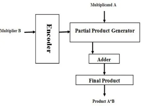
[image:3.595.333.531.484.638.2]3.1 Proposed and Modified Booth Algorithm: This algorithm consists of three major steps as shown in the proposed structure of booth algorithm figure that includes generation of partial product called as recoding, reducing the partial product in 2 rows, and addition that gives final result product. Here we know about each block of booth algorithm for multiplication process.
Fig-2: Proposed Algorithm
3.2 Brief Working Principle of Booth Algorithm: This modified booth multiplier is used to perform high-speed multiplications using modified booth algorithm. And this
multiplier’s computation time and the logarithm of the word length of operands are proportional to each other. Here we can reduce half the number of partial product. The radix-4 booth algorithm used here to increases the speed of multiplier and reduces the area of multiplier circuit. In this algorithm, every second column is taken and multiplied by 0 or +1 or +2 or -1 or -2 instead of multiplying with 0 or 1 after shifting and adding of every column of the booth multiplier. Thus, half of can be reduced using this booth algorithm. Based on the multiplier bits, the process of encoding the multiplicand (M) is performed by radix-4 booth encoder.
The overlapping is used for comparing three bits at a time. This grouping is started from least significant bit (LSB), in which only two bits of the booth multiplier are used by the first block and a zero is assumed as third bit as shown in the figure.
Fig-3: Bit Pairing as per Booth Recoding
The figure shows the functional operation of the radix-4 booth encoder that consists of eight different types of states. The outcomes or multiplication of multiplicand with 0, -1, and -2 are consecutively obtained during these eight states. Hence, to design n-bit parallel multipliers only n2 partial products are generated by using booth algorithm
Table 1. Booth Recoding Table for Radix-4
[image:3.595.41.275.531.708.2]© 2017, IRJET | Impact Factor value: 5.181 | ISO 9001:2008 Certified Journal | Page 547 flip flop. Which makes sure that timing violations does not
exist.
3.3 Adaptive Hold Logic:
The operation of the AHL circuit is as follows: when an input pattern arrives, both judging blocks will decide whether the pattern requires one cycle or more cycles to complete and pass both results to the multiplexer. It selects one of either result based on the output of the aging indicator. Then an OR operation is performed between the result of the multiplexer, and the Q signal is used to find the input of the D flip-flop & When the pattern requires one cycle, the output of the multiplexer is 1. The!(gating) signal will become 1, and the input flip flops will latch new data in the next cycle. When the output of the multiplexer is 0, which means the input pattern requires more than 1 cycles to complete, the OR gate output will 0 to the D flip-flop. The !(gating)signal will be 0 to disable the clock signal of the input flip-flops in the next cycle. Note that only a cycle of the input flip-flop will be disabled because the D flip-flop will latch 1 in the next cycle.
3.4 RAZOR FLIP FLOP:
One-bit Razor flip-flop contains shadow latch, flip-flop, mux and XOR gate,. The main flip-flop catches the execution result for the combination circuit using a normal clock signal, and shadow latch catches the executed result using a delayed clock signal, which is slower than the normal clock signal. If the latched bit of the shadow latch is different from that of the flip-flop, this means the path delay of the current operation exceeds the cycle period, and the main flip-flop catches an incorrect result.
If errors occur, the Razor flip-flop will set the error signal to one to notify the system to re-execute the operation and notify the AHL circuit that an error has occurred. We use Razor flip-flops to detect whether an operation that is considered to be a one-cycle pattern can really finish in a cycle. Otherwise the operation is re-executed with two cycles.
4. EXPERIMENTAL RESULTS
The Simulation result of Radix- Booth Multiplier consists of RTL level Schematic of overall circuit and individual circuit elements like Adaptive Hold Logic, Razor Flip Flop and Booth encoder etc. Apart from these the simulation results show that using radix-4 booth multiplier along with AHL and Razor Flip Flop execution time required by the multiplier is reduce for a considerable extent and it also shows that the load on circuit i.e average fanout is very less.
Fig-4: RTL Schematic of proposed model.
© 2017, IRJET | Impact Factor value: 5.181 | ISO 9001:2008 Certified Journal | Page 548 Fig-6: RTL Schematic showing Razor flip flop and booth
encoders.
Fig-7: RTL Schematic of AHL
Fig-8: RTL Schematic of Razor Flip Flop.
7.1 OUTPUT 1:
Fig-9: Simulation output in ISim.
OUTPUT 2:
© 2017, IRJET | Impact Factor value: 5.181 | ISO 9001:2008 Certified Journal | Page 549 Fig-11 : Total power used by proposed system.
Timing Summary:
Minimum period: 15.587ns
Minimum input arrival time before clock: 8.889ns Maximum output required time after clock: 16.992ns Maximum combinational path delay: No path found.
Table-2 Comparison of different multipliers performance in terms of speed Average fanout.
Aging aware Column
bypass multiplier. Aging aware Radix-4 Booth Multiplier.
Maximum output
required time after
clock. 39.676ns 16.992ns
Minimum input arrival
time before clock. 40.837ns 8.889ns
Average fanout of
non-clock nets. 3.73 2.99
Above results are obtained using Xilinx ISE 14.2 and above proposed architecture can be analysed using Spartan FPGA boards for real time implementation.
5. CONCLUSION AND FUTURE WORK
An Efficient multiplier is designed with Adaptive Hold Logic and Razor Flip Flop has been successfully simulated using Xilinx ISE 14.2. A modified radix-4 Booth multiplier design is to yield less number of partial products at output of multiplier. Apart from this, Booth algorithm considers the two’s complement of given input number making multiplication of signed / negative number as simple as positive one. Due to these advantages, there is considerable reduction in amount of area taken by multiplier circuit in the system making system compact, less delay and maximizing throughput. We can extend this work by employing Radix-8 Booth algorithm for partial products generation. Expected outcome is less number of partial products, reduced area & reduced delay.
Note that in addition to the BTI effect that increases transistor delay, interconnect also has its aging issue, which is called electromigration. It occurs when the current density is high enough to the drift of metal ions along the direction of electron flow. Future work can be carried out to reduce electromigration effect and multiplier design can be extended to any number of input / output combinations. REFERENCES
[1] Ing-Chao Lin, Member, IEEE, Yu-Hung Cho, and Yi-Ming Yang,
“Aging-aware reliable multiplier design with adaptive hold logic”, IEEE Transactions On Very Large Scale Integration (VLSI) Systems, vol. 23, no. 3, Mar. 2015
[2] Shubhangi Ramannawar, Deepak Kumar, “Efficient Multiplier Design
Using Modified Booth Algorithm and Razor Flip-Flop”, International Journal of Science, Engineering and Technology Research (IJSETR) Volume 1, Issue 1, Jan 2017.
[3] Y. Cao. (2013). Predictive Technology Model (PTM) and NBTI Model
[Online]. Available: http://www.eas. asu.edu/ptm
[4] S. Zafaret al., “A comparative study of NBTI and PBTI (charge trapping)
in SiO2/HfO2 stacks with FUSI, TiN, Re gates,” in Proc. IEEE Symp. VLSI Technol. Dig. Tech. Papers, 2006, pp. 23–25.
[5] S. Zafar, A. Kumar, E. Gusev, and E. Cartier, “Threshold voltage
instabilities in high-k gate dielectric stacks,” IEEE Trans. Device Mater. Rel., vol. 5, no. 1, pp. 45–64, Mar. 2005.
[6] H.-I. Yang, S.-C. Yang, W. Hwang, and C.-T. Chuang, “Impacts of
NBTI/PBTI on timing control circuits and degradation tolerant design in nano scale CMOS SRAM,” IEEE Trans. Circuit Syst., vol. 58, no. 6, pp. 1239–1251, Jun. 2011.
[7] R. Vattikonda, W. Wang, and Y. Cao, “Modeling and minimization of
pMOS NBTI effect for robust naometer design,” in Proc. ACM/IEEEDAC, Jun. 2004, pp. 1047– 1052.
[8] S. V. Kumar, C. H. Kim, and S. S. Sapatnekar, “NBTI aware synthesis of
digital circuits,” in Proc. ACM/IEEE DAC, Jun. 2007, pp. 370–375.
[9] A. Calimera, E. Macii, and M. Poncino, “Design techniques for NBTI
tolerant power-gating architecture,” IEEE Trans. Circuits Syst., Exp.Briefs, vol. 59, no. 4, pp. 249–253, Apr. 2012.
[10]K.-C. Wu and D. Marculescu, “Joint logic restructuring and pin
reordering against NBTI-induced performance.
[11]Y.-S. Su, D.-C. Wang, S.-C. Chang, and M. Marek-Sadowska,
“Performance” optimization using variable-latency design style,” IEEE Trans. Very Large Scale Integr. (VLSI) Syst., vol. 19, no. 10, pp. 1874– 1883, Oct. 2011.
[12] Y. Chen et al., “Variable-latency adder (VL- Adder) designs for low
power and NBTI tolerance,” IEEE Trans. Very Large Scale Integr. (VLSI) Syst., vol. 18, no. 11, pp. 1621–1624, Nov. 2010.
[13] Yongho Lee, Taewhan Kim,(2011) “A Fine-Grained Technique of
NBTI-Aware Voltage Scaling and Body Biasing for Standard Cell Based Designs” IEEE TRANSACTIONS ON VERY LARGE SCALE INTEGRATION (VLSI) SYSTEMS.
[14]Yu-Shih Su, Da-Chung Wang, Shih-Chieh Chang, and Malgorzata
Marek-Sadowska,(2011) “Performance Optimization Using Variable-Latency Design Style” IEEE Transactions On Very Large Scale Integration (VLSI) Systems, VOL. 19, NO. 10.
[15]Yiran Chen, Hai Li, Cheng-KokKoh, Guangyu Sun, Jing Li, Yuan Xie, and
Kaushik Roy,(2010) “Variable-Latency Adder (VL-Adder) Designs for Low Power and NBTI Tolerance” IEEE Transactions On Very Large Scale Integration (VlSI) Systems, VOL. 18, NO. 11
Shubhangi Ramannawar, received the Bachelor of Engineering in Electronics and Communication Engineering from BLDEA's V.P Dr P.G.
Halakatti College of Engineering & Technology, Bijapur,Karnataka, She is
currently pursuing M.Tech. (VLSI) from Department of Electronics & Communication Engineering, (VIST, Bhopal) Under Rajeev Gandhi Prodyogiki Visvavidhyalaya Bhopal, Madhya Pradesh, India. Her research interests include Low power and high performance VLSI design.