ISSN (Print) : 2320 – 3765 ISSN (Online): 2278 – 8875
I
nternational
J
ournal of
A
dvanced
R
esearch in
E
lectrical,
E
lectronics and
I
nstrumentation
E
ngineering
(An ISO 3297: 2007 Certified Organization) Website: www.ijareeie.com
Vol. 6, Issue 2, February 2017
NINE-LEVEL Multilevel Voltage Source
Inverter with Lower Number of Circuit Devices
A.Maideen Abdhulkader Jeylani1, A.Mahaboob Subahani2, A.C.Varishnee3, J.Priya Dharshini4
Assistant professor, Dept. of EEE, Sri Krishna College of Engineering & Technology, Coimbatore, Tamilnadu, India1
Assistant Professor, Dept. of EEE, PSG College of Technology, Coimbatore, Tamilnadu, India 2
PG Student [PED], Dept. of EEE, Sri Krishna College of Engineering & Technology, Coimbatore, Tamilnadu, India 3,4
ABSTRACT: An advanced configuration of multilevel inverter is being proposed. There are a umber of multilevel inverters available. In this cascaded H-bridge voltage source multilevel inverter is being implemented, it’s basically a nine level voltage source inverter which can generate the desired voltages with low number of circuit devices. The size of the proposed device is small compared to other types of multilevel voltage source inverter where nine power semiconductor switches and five dc voltage sources is used including power semiconductor switches and related gate driver circuits. The losses and voltage drops can be reduced more. For step input Multicarrier sinusoidal pulse width modulation (SPWM) technique is implemented. The sinusoidal step output can be observed through simulation and the voltage levels of the output can be calculated. The proposed device finds its application in for industrial motor drives, utility interfaces for renewable energy systems, flexible AC transmission system, high voltage direct current transmission and traction drives systems for controlling the systems.
KEYWORDS :Multilevel Inverter, Voltage drops, Sinusoidal Pulse Width Modulation.
I. INTRODUCTION
A multilevel inverter is a power electronic device which is capable of using multiple lower level DC voltages as an input for providing desired alternating voltage at the output. To generate the AC voltage from DC voltage mostly a three level inverter is used, it creates three different voltages for the load. IfVDCis the input given to the three level
inverter it produces +VDC/2,0 and –VDC/2 as output. These three newly generated voltages are switched usually to build
ISSN (Print) : 2320 – 3765 ISSN (Online): 2278 – 8875
I
nternational
J
ournal of
A
dvanced
R
esearch in
E
lectrical,
E
lectronics and
I
nstrumentation
E
ngineering
(An ISO 3297: 2007 Certified Organization) Website: www.ijareeie.com
Vol. 6, Issue 2, February 2017
II. INVERTER TOPOLOGY
An inverter converters the direct current(DC) to alternating current(AC) It usually also increases the voltage, inorder to increase the voltage, the current must be decreased, for this an inverter will use a lot of current on the DC side when only a small amount is being used on the AC side. There are a number of modulation techniques namely sinusoidal pulse width modulation, selective harmonic elimination and space vector modulation. The most promising and the latest of such a topology for high power applications is the Modular Multilevel Converter.The main aim of this master thesis project is to deeply investigate and evaluate one of them, based on a carrier phase shifted PWM techinique. The four different control topologies used here has three loops of control namely, Averaging Control based on the currents inside the converter, Individual Balancing Control based on the output current and capacitors voltages, and Arm Balancing Control based on the voltage difference between the arms of the converter. Here a switching frquency that meets the two required criteria: low enough to maintain cost feasibility and high enough to reach a harmonic performance target. Here an additional proposal is been made where an analytic expression for the output voltage spectrum of the converter, which enables prediction of harmonic performance.
1.Diode clamped multilevel inverter : A neutral point clamped inverter is the first invention in multilevel converters, it was initially proposed as a three level inverter. The principle of diode clamping can extended to any level. The diode clamped inverter focuses more on low frequency applications. Diodes are used here to limit power devices voltge stress. The output voltage distortion is very low due to multiple levels in the output voltages. The dv/dt of switches is low since the switches used to reduce voltage, the switches can operate at a lower switching frequency. The common mode voltages are reduced and the input currents have low distortions in application motor drives.
Fig.1 Diode clamped multilevel inverter
ISSN (Print) : 2320 – 3765 ISSN (Online): 2278 – 8875
I
nternational
J
ournal of
A
dvanced
R
esearch in
E
lectrical,
E
lectronics and
I
nstrumentation
E
ngineering
(An ISO 3297: 2007 Certified Organization) Website: www.ijareeie.com
Vol. 6, Issue 2, February 2017
3.Cascaded H-Bridge multilevel inverter : The cascaded multilevel inverter is based on the series connection of single leg or double leg (H-bridges) inverters with separate DC sources or capacitors. There are several switching states, the single leg unit has 2 states for each of the two possible currents directions while the double unit has 4 states.
Fig 3. Cascaded H-Bridge multilevelinverter
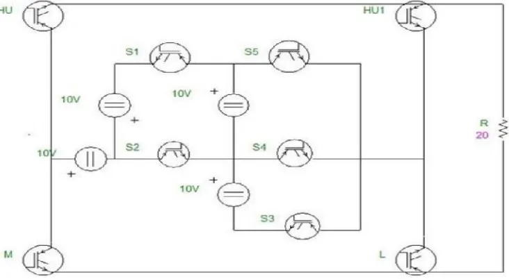
4. NEW TOPOLOGY FOR MULTILEVEL INVERTER :New topology for multilevel inverter is nine level multilevel inverter and four DC voltage sources. The desired output voltage can be obtained by the gate signal for transistors are given by Multicarrier Sine Pulse Width Modulation technique. The resistive loads are connected in parallel with AC load. The resistance of the load is 20 ohm.
ISSN (Print) : 2320 – 3765 ISSN (Online): 2278 – 8875
I
nternational
J
ournal of
A
dvanced
R
esearch in
E
lectrical,
E
lectronics and
I
nstrumentation
E
ngineering
(An ISO 3297: 2007 Certified Organization) Website: www.ijareeie.com
Vol. 6, Issue 2, February 2017
COMPARISON TABLE :The comparison table compares the existing system and proposed system.
S. NO EXISTING SYSTEM PROPOSED SYSTEM
SWITCHES 10 9
PWM SINE PWM MULTICARRIER SPWM
Table1. Comparison Table
Here ten switches and sine PWM technique is being used in the existing system, where as in the proposed system uses only nine switches and multicarrier PWM technique is used. The efficiency level can be increased upto 93% whereas in proposed system the efficiency level can be increased upto 96% using lower number of power semiconductor switches. In existing system only one reference signal and carrier signal is used whereas in proposed system several reference signals and only one carrier signal.
III.PWM TECHNIQUE
The single pulse width modulation can be used to convert the reference signal to the square wave signal.There is only one pulse per half cycle and the output rms voltage is changed by varying the width of the pulse.The gating signals are generated by comparing the rectangular control signal amplitude with triangular carrier signal signal amplitude. The frequency of the control signal determines the fundamental frequency of ac output voltage. The reference signal is obtained to the zero crossing circuits. The amplitude modulation index is defined asma= Ar/ Acis also reffered as control
variable where Arthe amplitude of reference or rectangular signal and Ac is the amplitude of the carrier wave.
Ar(reference amplitude) can be varied from 0 to Ac,and the pulse width can be varied from 0 to 100 percent. The
transistor works as a switch which is turned on and off by varying the generated gating signals. Adding several pulses in each of the half cycles of output voltage helps to reduce the harmonics.The number of pulses added per half cycle is determined by carrier frequency Fc. The output voltage is controlled by modulation index ma . This type of modulation
ISSN (Print) : 2320 – 3765 ISSN (Online): 2278 – 8875
I
nternational
J
ournal of
A
dvanced
R
esearch in
E
lectrical,
E
lectronics and
I
nstrumentation
E
ngineering
(An ISO 3297: 2007 Certified Organization) Website: www.ijareeie.com
Vol. 6, Issue 2, February 2017
IV. SIMULATION RESULT AND DISCUSSION
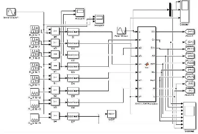
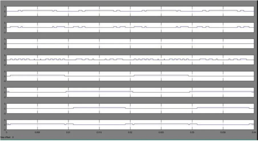
In the fig.9. Pulse generated for semiconductor switches using multicarrier PWM is shown these pulses are given to the corresponding nine semiconductor switches.
Fig. 5Generated PWM pulse
SIMULATION CIRCUIT DIAGRAM:
In this fig. 10 has been shown the simulation of the nine level multilevel inverter with reduced number of circuit compenets with R load. Since it is resistive load the output is in phase.
ISSN (Print) : 2320 – 3765 ISSN (Online): 2278 – 8875
I
nternational
J
ournal of
A
dvanced
R
esearch in
E
lectrical,
E
lectronics and
I
nstrumentation
E
ngineering
(An ISO 3297: 2007 Certified Organization) Website: www.ijareeie.com
Vol. 6, Issue 2, February 2017
INPUT and OUTPUT :
In fig.7DC input is given based on the voltage levels of nine level multilevel inverter. 10V is given for input signal and the output signal may differ.In fig.8 the output of current and voltage level is verified. The voltage level is 40V and the current level is 2amps. The current signal is in the form of sinusoidal signal and the voltage signal is in the form of sinusoidal step output signal.
Fig.7 Input voltage Fig.8 Output waveform
PWM PULSES :
ISSN (Print) : 2320 – 3765 ISSN (Online): 2278 – 8875
I
nternational
J
ournal of
A
dvanced
R
esearch in
E
lectrical,
E
lectronics and
I
nstrumentation
E
ngineering
(An ISO 3297: 2007 Certified Organization) Website: www.ijareeie.com
Vol. 6, Issue 2, February 2017
SWITCHING STATES : DC OUTPUT
VOLTAGE H1 M S1 S2 Hu L S11 S22 Hu1
3VDC 1 0 0 0 1 1 0 1 0
2VDC 1 0 0 0 1 1 1 0 0
1VDC 0 0 0 0 1 1 1 1 0
0 0 0 0 0 0 1 0 0 1
-1VDC 0 1 0 0 0 0 1 1 1
-2VDC 1 1 0 0 0 0 1 0 1
-3VDC 0 1 1 0 0 0 0 1 1
Table .2 Switching states
In Table 2 they are the switching states of semiconductor switches shown in the circuit. When the switch is 1 the device will turn ON and if the switch is 0 then device will turn OFF.
V. CONCLUSION
Proposal of an advanced configuration for symmetrical MVSI (Multilevel Voltage Source Inverter) is taken as the main contribution of this paper. The number of power semiconductor switches and the gate driver circuits has been reduced. Because of the reduced switch count the poer losses have been reduced. The comparitive study among the suggested inverter, CHB(Cascaded H-Bridge) and recently proposed converters shows the superiority of the proposed inverter over the mentioned topologies. By reducing the no.of devices there is a substancial reduction in the total costs with a simpler control scheme. The simulation reslts shows the feasibility of the proposed configuration.
VI. FUTURE SCOPE
When compared to other multilevel inverters the proposed inverter, voltage drops and losses can be reduced more. The efficiency level of the inverter can be increased to maximum level through advanced level of heric topology. The voltage can be increased to maximum by using power semiconductor switches. An advanced level of topology can be introduced to make the device more simple and also the voltage losses can be controlled easily.Without using multicarrier spwm technique, the losses and voltage drops can be reduced and also the efficiency can be increased to maximum.
REFERENCES
[1]Mohammad Reza JannatiOskuee, SajadNajafiRavadanegh, “An Innovative Scheme of Symmetric Multilevel Voltage Source Inverter with Lower Number of Circuit Devices”, IEEE Transactions on Industrial Electronics, Vol. 62, No. 11, November 2015.
[2]P. Vinod Kumar, Ch. Santosh Kumar, And K. Ramesh Reddy,” Single Phase Cascaded Multilevel Inverter Using Multicarrier PWM Technique” Vol. 8, No. 10, October 2013, Issn 1819-6608, Arpn Journal of Engineering And Applied Sciences
[3]A.L.Batschauer,S.A.Mussa,AndM.L.Heldwein,“Three Phase hybrid Multilevel Inverter Based on Half Bridge Modules,”IEEE Trans. Ind. Electron.,Vol.59, No. 2,Pp. 668–678,Feb.2012.
[4]M.R.Banaei, M.R.JannatiOskuee, And F.M.Kazemi,“A new Advanced Topology of Stacked Multicell Inverter,”Int.J.EmergingElect.Power Syst.,Vol.15, No. 4,pp. 327–333,2014.
[5]A. K.Sadigh,S.H. Hosseini, M.SabahiandG.B.Gharehpetian,“Double Flying Capacitor Multicell Converter Based on Modified Phase Shifted Pulse WidthModulation,”IEEETrans.PowerElectron.,Vol.25,No.6,pp.1517-1526, Jun.2010.
[6]M.G.H.Aghdam,S.H.FathiandG.B.Gharehpetian, “A Novel Switching Algorithm to Balance Conduction Losses in Power Semiconductor Devices of Full-Bridge Inverters, ”Eur.Trans.Elect.Power,Vol.18,No.7, pp. 694– 708,Oct. 2008.
[7]A.Ajami,A.Mokhberdoran,andM.R.J.Oskuee,“A New Topology of Multi level Voltage Source Inverter to Minimize the Number of Circuit Devices and Maximize the Number of output Voltage Levels,”J.Elect.Eng. Technol.,Vol.8,No.6,Pp.1321–1329,Nov.2013.
[8]B. R. Lin and H. H. Lu (2000), “A novel PWM scheme for single-phase three-level power-factor-correction circuit,” IEEE Transactions on Industrial Electronics., vol. 47, no. 2, pp. 245-252.