Publisher: Asian Economic and Social Society
A Novel DC-DC Boost Converter Design for Higher Conversion Efficiency
Samer AlSadi (Electrical Engineering department, Faculty of Engineering and Technology, Palestine Technical University-Kadoorie , Tulkarm, Palestine)
Tamer Khatib (Department of Electrical, Electronic & System Engineering, Faculty of Engineering & Built Environment, Universiti Kebangsaan Malaysia, Bangi 43600, Selangor, Malaysia)
Author (s)
Samer AlSadi Electrical Engineering department, Faculty of Engineering and Technology, Palestine Technical University-Kadoorie , Tulkarm, Palestine.
E-mail: [email protected]
Tamer Khatib Department of Electrical, Electronic & System Engineering, Faculty of Engineering & Built Environment, Universiti Kebangsaan Malaysia, Bangi 43600, Selangor, Malaysia.
E-mail: [email protected]
A Novel DC-DC Boost Converter Design for Higher Conversion Efficiency
Abstract
This paper presents the development of a DC-DC boost converter. In the proposed boost converter design, a passive regenerative snubber circuit is included to absorb the energy of stray inductance so as to reduce the IGBT switching losses. MATLAB simulation as well as an experiment results are conducted to validate the proposed device. The results show that the proposed boost converter design gives an efficiency of 93% which is better than the conventional converter (88%).
Keywords: Boost Converter; chopper; DC-DC converters
Introduction
A boost converter (step-up converter) is a power converter with an output DC voltage greater than its input DC voltage. It is a class of switching-mode power supply (SMPS) containing at least two semiconductor switches (a diode and a transistor) and at least one energy storage element. Filters made of capacitors (sometimes in combination with inductors) are normally added to the output of the converter to reduce output voltage ripple (Rashid, 2001).
Boost converter operation may cause serious reverse-recovery problems and increase the rating of all devices. As a result, the conversion efficiency is degraded and may result in severe electromagnetic interference problem under this situation (Khatib, 2010, Khatib, 2010(1), AlSadi, 2012, Mohan, 1995, Jovanovic, 1999, Duarte, 2002).. To overcome the severe reverse-recovery problem of high voltage diodes, voltage-clamped technique is manipulated in the converter design. However,
this technique causes voltage stress on the switches and voltage gain is limited by the turn-on time of the auxiliary switch (Khatib, 2010, Khatib, 2010(1), Mohan, 1995, Jovanovic, 1999, Duarte, 2002, Roh, 2003). Another problem in boost converter operation is the leakage energy of the storage inductor which is generated by the turning off action of the converter switches. It will result in a high-voltage ripple across the switch due to the resonant phenomenon induced by the leakage current. Therefore, to protect the converter switching devices, two mitigating actions can be taken, that is, by using a high voltage rating device with a snubber circuit and by depleting the inductor leakage energy. In order to increase the conversion efficiency, many modified boost converter topologies have been investigated (Roh, 2003, Zhao, 2003, Tseng, 2004).
and sink the leakage energy of the inductor during transient switching.
Proposed Boost Converter
A boost converter is the front-end component of a PV system connected between a PV array and a load. It is basically a power converter with DC output voltage greater than its input voltage. It is a class of switching-mode power supply containing at least two semiconductor switches, a diode and a transistor and at least one energy storage element. Filters made of capacitors in combination with inductors are normally added to the output of the converter to reduce the output voltage ripple (Rashid, 2001). An inherent problem in boost converters is that it may cause serious reverse recovery problem which may increase the rating of devices and degrade the conversion. To increase the conversion efficiency, an improvement is made in the boost converter design. Figure 1 shows the MPPT controller with the proposed boost converter design. The converter consists of an inductor in the primary side (L), clamping diodes, D1,D2, capacitor C2 used to form a regenerative circuit to sink the reverse recovery current and an output filter circuit using diode, Do and capacitor, Co.
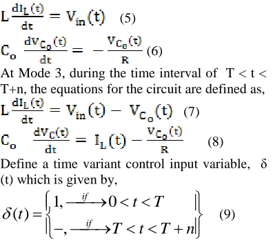
To describe the operation of the boost converter, four modes of operation are considered. Figure 2 shows the triggering signal of the converter’s switch operating at the four modes of operation.
1. Mode 2 operation - In this mode, the switch Q is turned off and the current, IL will start to charge the parasitic capacitor of the switch Q as shown in Fig. 3b. When the switch voltage is greater than the clamped capacitor voltage, VC1, the clamping diode, D1 will conduct and transmit the energy of the leakage inductor LK into the clamped capacitor, C1. C1 is assumed to be large enough with favorable high frequency response so that its voltage, VC1 can be viewed as a stable DC output with low ripple for clamping the maximum value of the switch voltage. In addition, D1 should be a fast conductive device with voltage rating similar to the Switch Q.
2. Mode 3 operation – this mode of operation is illustrated as in Fig. 3c in which the switch is turned off and the reverse parasitic voltage of the output diode, Do decays to zero. At this time, Do starts to conduct and the rectifier diode, D2 is cut off. The series voltages, VLK and VLm will charge the output capacitor, Co and supply current to the load.
3. Mode 4 operation - At this time, the switch Q is turned on (Figure 3d) and the clamping diode, D1 is cut off promptly without reverse recovery current because it has a low voltage. The switch Q is turned on under zero current switching because the current, I1 is limited by the leakage inductor, Lk and it cannot derive any current from the inductor side or the passive regenerative snubber circuit side. This soft switching is helpful for reducing the switching losses.
Boost Converter Analysis
For boost converter analysis, the Mode 1 and Mode 3 operations for the ON and OFF switching states respectively are taken into consideration. As the switching boost converter is time variant and topology variant, the defining equations of the circuit are put in the following forms (Xu, 1991).
At Mode 1, during the time interval of 0 < t < T, it can be observed that,
(5)
(6)
At Mode 3, during the time interval of T < t < T+n, the equations for the circuit are defined as,
(7)
(8)
Define a time variant control input variable, δ (t) which is given by,
n
T
t
T
T
t
t
if if,
0
,
1
)
(
(9)the time variant and topology variant circuit becomes,
(10)
(11)
To perform DC steady state and AC small signal analysis, the variables
are defined as having two components which are the DC component and the corresponding perturbation component (Rashid, 2001). If the DC components are represented by the letters with non hat symbol and the perturbation components are represented by the letters with hat symbol, equations (10) and (11) become,
(12)
(13)
where, D is the duty cycle. To perform DC steady state analysis, let
and .
Then equations (12) and (13) become,
(14)
(15)
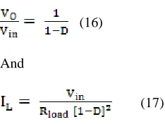
From equations (14) and (15), the relation between the input and the output voltages of the boost converter will be:
(16)
And
(17)
Assuming that the converter is ideal in which output power is equal to the input power,
, we get,
(18)
Substituting equation (15) into (17), we get the current gain equation of the boost converter which is given by,
(19)
Results and discussion
A MATLAB simulink of the boost converter was done by considering the converter component values of C1 = 6.8 µF, Co = 680 µF and L=9 µH based on the equations (12) and (13), D1, D2 and Do are the Schottky diodes and Q is a MOSFET IRFP2907, with frequency ƒ = 20 kHz. The performance of the proposed converter is tested using a 25V/300 Watt load. Figure 5.3a shows the output current and voltage of the boost converter. It is noticed that both, the voltage and the current reached their steady state values in .2 seconds. Figure 4 shows the duty cycle of the triggering signal, the duty the duty cycle is 20%.
Figures 6 and 7 show the converter simulation results in terms of its voltage gain ( ) and efficiency ( ), respectively. As for the voltage gain of the proposed boost converter, the added capacitor, C1 does not seem to affect the voltage gain because it is in parallel with the output capacitor at the reverse mode of operation. The maximum efficiency of the converter is approximately 93%, for the converter to drive a 100 - 800 W load and thus the converter is considered to be efficient compared with the conventional boost converter with an efficiency of 88% (Mohan, 1995). The performance of the boost converter is first tested by using the oscilloscope to measure the output voltage and the duty cycle of the converter. A 20 A current probe is also used to measure the output current. Figure 8 shows the boost converter output voltage at the solar noon in which the output voltage is 25 V for an input voltage of 21.2 volt. The output current is 10.2 A and the calculated conversion efficiency is 90.9 %. Figure 9 shows the duty cycle of the triggering signal which is found to be 28 % (14μs/50μs).
real test is higher than the one obtained from the simulation. The differences in the results are due to the assumption made in simulation which considers ideal circuit elements and no losses. The input and the output voltages are almost same where the output power is slightly different. The difference in the output power is due to the variation in the load. The load in the simulation is exactly 300 Watt where in real test the load varies.
Conclusion
In this paper, a novel boost converter was presented. A snubber circuit has been added to reduce the IGBT switching losses by absorbing
the energy of stray inductance. The sunnber circuit is consisted of two diodes and two capacitors. However, MATLAB simulation as well as an experiment results have been performed in order to test the proposed boost converter. The results showed that the proposed boost converter design has a better efficiency of about 93% compared to the conventional converter with efficiency of 88%.
Figure-1 Proposed boost converter
Figure-3a Mode 1 operation of boost converter
Figure-3 b Mode 2 operation of boost converter
Figure-3 c Mode 3 operation of boost converter
Figure-3 d Mode 4 operation of boost converter
Figure-4 Output voltage and current of the boost converter for a 25V/300W load
Figure-6 Voltage gain of the proposed boost converter
Figure-7 Boost converter efficiency
Figure-9 Duty cycle of the converter during testing
Table-1 Comparing the simulation and experimental results of the boost converter Simulation Experimental
Output voltage 25 V 24.9V
Input voltage 21 V 21.2 V
Output power 300 Watt 249 Watt
Conversion efficiency 92.6 % 90.9 %
Duty cycle 20% 28%
References
AlSadi, S, Khatib, T., Malloh, S. (2012) Development of a novel solar radiation measuring device. J. of Asian Scientific Research. Vol. 2. No.2, pp 40-44
Duarte, C, Barbi, I., (2002). An improved family of ZVS-PWM active clamping DC-to-DC converters, IEEE Trans. Power Electron.Vol. 17, no. 1, pp. 1–7.
Jovanovic, M., Jang Y (1999). A new soft-switched boost converter with isolated active snubber, IEEE Trans. Ind. Appl.. Vol. 35, pp. 496–502.
Khatib, T., A. Mahmoud, A., N. Amin, N, Sopian, K. (2010) An efficient maximum power point tracking controller for PV systems using new boost converter design and improved control algorithm. WSEAS Transaction on Power Systems. Vol.5, No. 2. pp.53-63.
Khatib, T., Mohamed, A., Mahmoud, M., Amin, N. (2010). An efficient maximum power point tracking controller Power Point Tracking Controller for a Standalone Photovoltaic System. International Review on Modelling and Simulation. Vol. 3, No.2. pp.129 -139.
Mohan, N., Undeland, T., Robbins, W., (1995). Power Electronics: Converters, Applications, and Design. Wiley,
Rashid, M., (2001) Power Electronics Handbook. Florida ACADEMIC PRESS, Roh, C, Han, S., Youn, M., (1999). Dual coupled inductor fed isolated boost converter for low input voltage applications, Electron. Lett., Vol. 35, pp. 1791–1792.
Tseng K., Liang, T., (2004). Novel high-efficiency step-up converter, Proc. Inst. Elect. Eng. Vol. 151, pp. 182–190.
Xu, J. (1991). An Analytical Technique for the Analysis of Switching DC-DC Converters, International Symposium on Circuits and Systems Vol. 2. pp 1212 - 1215.