ISSN(Online): 2320-9801
ISSN (Print): 2320-9798
I
nternational
J
ournal of
I
nnovative
R
esearch in
C
omputer
and
C
ommunication
E
ngineering
(An ISO 3297: 2007 Certified Organization) Website: www.ijircce.com
Vol. 5, Issue 1, January 2017
Analysis of High Speed Energy-Efficient
Carry Skip Adder High-Speed Skips Logic at
Different Levels
Shadab Ahmad1, Prof. Suresh S Gawande2, Prof. Sher Singh3
PG Student( VLSI Design), Dept. of ECE, Bhahbha Engineering Research Institute, Bhopal, MP, India1 Asst. Professor, Dept. of ECE, Bhahbha Engineering Research Institute, RGPV, Bhopal, MP, India 2,3
ABSTRACT: A carry skip adder (CSKA) structure has the high speed and very low power consumption. The speed of the structure is achieved by concatenation of all the blocks. The incrimination blocks are used to improve the efficiency of the carry skip adder structure. In existing method multiplexer logic is used, the proposed structure uses the AND-OR-Invert (AOI) and OR-AND-Invert (OAI) for the skip logic. This work uses a simple and efficient gate-level modification to significantly reduce the area and power of the CSLA. Based on this modification 8-, 16-, 32-, and 64-b square-root CSLA (SQRT CSLA) architecture. The speed enhancement is achieved by combining concatenation and incrementation schemes to conventional CSKA (Conv-CSKA) structure. In addition, instead of utilizing multiplexer logic, the proposed structure makes use of AND-OR-Invert (AOI) and OR-AND-Invert (OAI) compound gates for the skip logic. The structure may be realized with both fixed stage size (FSS) and variable stage size (VSS) styles, wherein the latte r further improves the speed and energy parameters of the adder. Finally
KEYWORDS: Carry skip adder (CSKA), energy efficient, high performance, hybrid variable latency Adders, voltage scaling
I. INTRODUCTION
ISSN(Online): 2320-9801
ISSN (Print): 2320-9798
I
nternational
J
ournal of
I
nnovative
R
esearch in
C
omputer
and
C
ommunication
E
ngineering
(An ISO 3297: 2007 Certified Organization) Website: www.ijircce.com
Vol. 5, Issue 1, January 2017
are given in [2]. Comparisons between different types of adders in terms of area, delay, and power dissipation are provided in [3-5].
Design of area and power efficient high speed data path logic systems are one of the most substantial areas of research in VLSI system design. In digital adders, the speed of addition is limited by the time required propagate a carry through the adder. The sum for each bit position in an elementary adder is generated sequentially only after the previous bit position has been summed and a carry propagated into the last position. One of the effective techniques to lower the power consumption of digital circuits is to reduce the supply voltage because of quadratic dependence of the switching energy on the voltage. Moreover, the sub threshold current, that is the main leakage component in OFF devices, has an exponential dependence on the supply voltage level through the drain-induced barrier lowering impact. Depending on the amount of the supply voltage reduction, the operation of ON devices might reside in the super threshold, near-threshold, or sub threshold regions. Working in the super threshold region provides us with lower delay and higher switching and leakage powers compared with the near/sub threshold regions. In the sub threshold region, the gate delay and leakage power exhibit exponential dependences on the supply and threshold voltages. Moreover, these voltages are (potentially) subject to process and environmental variations in the nano-scale technologies. The variations increase uncertainties in the said performance parameters. Additionally, the small sub threshold current causes a large delay for the circuits operating in the sub threshold region.
II. THEORY
A. MULTIPLEXERS
A Multiplexer is a device that allows one of several analog or digital input signals which are to be selected and transmits the input that is selected into a single medium. Multiplexer is also known as Data Selector. A multiplexer of 2n inputs has n select lines that will be used to select input line to send to the output. Multiplexer is abbreviated as Mux. MUX sends digital or analog signals at higher speed on a single line in one shared device. It recovers the separate signals at the receiving end. The Multiplexer boosts or amplifies the information that later transferred over network within a particular bandwidth and time. This article gives an overview of what is multiplexer and types of multiplexer.
ISSN(Online): 2320-9801
ISSN (Print): 2320-9798
I
nternational
J
ournal of
I
nnovative
R
esearch in
C
omputer
and
C
ommunication
E
ngineering
(An ISO 3297: 2007 Certified Organization) Website: www.ijircce.com
Vol. 5, Issue 1, January 2017
The Multiplexer acts as a multiple-input and single-output switch. Multiple signals share one device or transmission conductor such as a copper wire or fibre optic cable. In telecommunications, the analog or digital signals transmitted on several communication channels by a multiplex method. These signals are single-output higher-speed signals. A 4-to-1 multiplexer contains four input signals and 2-to-1 multiplexer has two input signals and one output signal.
Fig 2 Schematic Symbol for Multiplexer
Table 1:- Truth Table for 2 to 1 Multiplexer
I1 I0 A D
0 0 0 0
0 0 1 0
0 1 0 0
0 1 1 1
1 0 0 1
1 0 1 0
1 1 0 1
1 1 1 1
B. CONVENTIONAL CARRY SKIP ADDER
The structure of an N-bit Conv-CSKA, which is based on blocks of the RCA (RCA blocks), is shown in Fig. 1. In addition to the chain of FAs in each stage, there is carry skip logic. For an RCA that contains N cascaded FAs, the worst propagation delay of the summation of two N-bit numbers, A and B, belongs to the case where all the FAs are in the propagation mode. It means that the worst case delay belongs to the case where
Pi= Ai⊕Bi=1 for i= 1, . . ., N
ISSN(Online): 2320-9801
ISSN (Print): 2320-9798
I
nternational
J
ournal of
I
nnovative
R
esearch in
C
omputer
and
C
ommunication
E
ngineering
(An ISO 3297: 2007 Certified Organization) Website: www.ijircce.com
Vol. 5, Issue 1, January 2017
Fig 3. Conventional structure of the CSKA
III.METHOD
A. CARRY LOOK AHEAD ADDER (CLA)
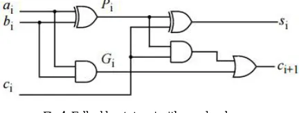
The carry look ahead adder (CLA) solves the carry delay disadvantage by calculative the carry signals before, based on the input signals. It’s based on the particular fact that a carry signal are generated in two cases:
(1) Once each bits ai and bi are one, or
(2) Once one of the two bits is one and so the carry-in is one.
Thus, one will write.
The above two equations can be written in terms of two new signals pi and gi , which are shown in Figure 4:
Fig 4: Full adder at stage i with pi and gi shown
ISSN(Online): 2320-9801
ISSN (Print): 2320-9798
I
nternational
J
ournal of
I
nnovative
R
esearch in
C
omputer
and
C
ommunication
E
ngineering
(An ISO 3297: 2007 Certified Organization) Website: www.ijircce.com
Vol. 5, Issue 1, January 2017
Fig. 5 Carry Look Ahead
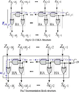
This structure is formed by combining concatenation and the incrimination schemes with the Conv-CSKA structure, which is shown in fig.3 and hence, is denoted by CI-CSKA. It provides us with the ability to use simpler carry skip logics. The logic replaces 2:1 multiplexers by AOI/OAI compound gates (Fig. 6). The gates, which consist of fewer transistors, have lower delay, area, and smaller power consumption compared with those of the 2:1 multiplexer. Note that, in this structure, as the carry propagates through the skip logics, it becomes complemented. Therefore, at the output of the skip logic of even stages, the complement of the carry is generated. The structure has a considerable lower propagation delay with a slightly smaller area compared with those of the conventional one. Note that while the power consumptions of the AOI (or OAI) gate are smaller than that of the multiplexer, the power consumption of the proposed CI-CSKA is a little more than that of the conventional one. This is due to the increase in the number of the gates, which imposes a higher wiring capacitance (in the noncritical paths).
ISSN(Online): 2320-9801
ISSN (Print): 2320-9798
I
nternational
J
ournal of
I
nnovative
R
esearch in
C
omputer
and
C
ommunication
E
ngineering
(An ISO 3297: 2007 Certified Organization) Website: www.ijircce.com
Vol. 5, Issue 1, January 2017
IV.RESULT
The result analyses of the CSKA and simulation results of the projected system are shown in following figure. The design planned in this paper has been developed victimization MODEL machine. ADDERS are a main building block in ALUs (arithmetic and logic units).Low power arithmetic circuits turn into very necessary in VLSI industry. Adder circuit is that the main building block in DSP processor.
Fig. 8 Block diagram of modified CSKA
Block diagram representation of the Hybrid or proposed model of the CSKA system shown in Figure 8 in which we see three input and two output which is represented in as a sum and carry of the model which is represented as a S and Co.
ISSN(Online): 2320-9801
ISSN (Print): 2320-9798
I
nternational
J
ournal of
I
nnovative
R
esearch in
C
omputer
and
C
ommunication
E
ngineering
(An ISO 3297: 2007 Certified Organization) Website: www.ijircce.com
Vol. 5, Issue 1, January 2017
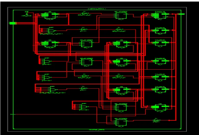
Fig. 10Technology schematic
ISSN(Online): 2320-9801
ISSN (Print): 2320-9798
I
nternational
J
ournal of
I
nnovative
R
esearch in
C
omputer
and
C
ommunication
E
ngineering
(An ISO 3297: 2007 Certified Organization) Website: www.ijircce.com
Vol. 5, Issue 1, January 2017
Figure 11 represents the simulation results come after the applied schematic digram as all Parameters applied on it. Simulation result is comes out by the use of Xilinx software.
V. CONCLUSION
In this paper, a static CMOS CSKA structure known as CI-CSKA was proposed, that exhibits a higher speed and lower energy consumption compared with those of the conventional one. In addition, AOI and OAI compound gates were exploited for the carry skip logics. The efficiency of the proposed structure for both FSS and VSS was studied by comparing its power and delay with those of the Conv-CSKA, RCA, CIA, SQRT-CSLA, and KSA structures. The results revealed considerably lower PDP for the VSS implementation of the CI-CSKA structure over a wide range of voltage from super-threshold to near threshold. The results also suggested the CI-CSKA structure as a very good adder for the applications where both the speed and energy consumption are critical. In addition, a hybrid variable latency extension of the structure was proposed.
REFERENCES
1. Milad Bahadori, Mehdi Kamal, Ali Afzali-Kusha “High-Speed and Energy-Efficient Carry Skip Adder Operating Under a Wide Range of
Supply Voltage Levels”, IEEE Transactions On Very Large Scale Integration (VLSI) Systems 2015.
2. Yajuan He., Chip-Hong Chang “A Power-Delay Efficient Hybrid Carry-Look ahead/Carry-Select Based Redundant Binary To Two’s
Complement Converter”, IEEE Transactions On Circuits And Systems—I: Regular Papers, Vol. 55, No. 1, February 2008.
3. By Dejan Markovic, Cheng C. Wang, Louis P. Alarco´n “Ultralow-Power Design in Near-Threshold Region”, IEEE • March 2010.
4. By Ronald G. Dreslinski, Michael Wieckowski, David Blaauw “Near-Threshold Computing: Reclaiming Moore’s Law Through Energy
Efficient Integrated Circuits”, IEEE Vol. 98, 0018-9219/$26.00 2010 IEEE No. 2, February 2010.
5. Shailendra Jain, Surhud Khare, Satish Yada, Ambili V “A 280mV-to-1.2V Wide-Operating-Range IA-32 Processor in 32nm CMOS”, IEEE
International Solid-State Circuits Conference feb 2012.
6. I. Koren, Computer Arithmetic Algorithms, 2nd ed. Natick, MA, USA: A K Peters, Ltd., 2002.
7. R. Zlatanovici, S. Kao, and B. Nikolic, “Energy–delay optimization of 64-bit carry-look ahead adders with a 240 ps 90 nm CMOS design example,” IEEE J. Solid-State Circuits, vol. 44, no. 2, pp. 569–583, Feb. 2009.
8. S. K. Mathew, M. A. Anders, B. Bloechel, T. Nguyen, R. K. Krishnamurthy, and S. Borkar, “A 4-GHz 300-mW 64-bit integer execution ALU
with dual supply voltages in 90-nm CMOS,” IEEE J. Solid-State Circuits, vol. 40, no. 1, pp. 44–51, Jan. 2005.
9. V. G. Oklobdzija, B. R. Zeydel, H. Q. Dao, S. Mathew, and R. Krishnamurthy, “Comparison of high-performance VLSI adders in the
energy-delay space,” IEEE Trans. Very Large Scale Integr. (VLSI)Syst., vol. 13, no. 6, pp. 754–758, Jun. 2005.
10. B. Ramkumar and H. M. Kittur, “Low-power and area-efficient carry select adder,” IEEE Trans. Very Large Scale Integr. (VLSI) Syst., vol. 20,
no. 2, pp. 371–375, Feb. 2012.
11. M. Vratonjic, B. R. Zeydel, and V. G. Oklobdzija, “Low- and ultra low-power arithmetic units: Design and comparison,” in Proc. IEEE Int.
Conf. Comput. Design, VLSI Comput. Process. (ICCD), Oct. 2005, pp. 249–252.
12. C. Nagendra, M. J. Irwin, and R. M. Owens, “Area-time-power tradeoffs in parallel adders,” IEEE Trans. Circuits Syst. II, Analog Digit. Signal