Interface of a HVDC Converter Station for Weak AC Systems. (Under the direction of Dr. Subhashish Bhattacharya).
The high voltage direct current (HVDC) converter is a nonlinear load that injects harmonic currents back into the AC network that it is connected to. Harmonic distortion is, thus, a major issue for HVDC converter stations since it can adversely affect the voltage quality and cause malfunctioning of the equipment and loads that are connected to the AC grid. Hybrid active filters (HAF) are able to overcome the resonance and detuning issues of passive filters as well as the rating problems of pure active filters.
A HAF topology is proposed in this thesis that combines a damped double tuned passive filter with an active filter. The passive filter is tuned to remove the dominant harmonics and also the higher frequency currents while also providing reactive power support to the HVDC converter. The active filter is connected to the passive filter in a way that ensures minimal fundamental voltage across it and also that the fundamental current is diverted away from it through the passive branch, thereby reducing the active filter rating. The control of the active filter is done using a proportional-resonant regulator in the
synchronous reference frame. This method allows the compensation of the positive sequence and negative sequence dominant harmonics using a single controller.
by
Akash M. Gujarati
A thesis submitted to the Graduate Faculty of North Carolina State University
in partial fulfillment of the requirements for the degree of
Master of Science
Electrical Engineering
Raleigh, North Carolina 2014
APPROVED BY:
_____________________________ Dr. Subhashish Bhattacharya Chair of Advisory Committee
BIOGRAPHY
ACKNOWLEDGMENTS
I would like to thank my family for their support and contributions.
TABLE OF CONTENTS
LIST OF TABLES ... vi
LIST OF FIGURES ... vii
CHAPTER 1 Introduction ... 1
CHAPTER 2 Harmonic Distortion ... 4
2.1 Background ... 4
2.2 Harmonic Generation ... 4
2.3 Effects of Harmonic Distortion ... 9
2.4 Harmonic Filters ... 11
2.4.1 Single tuned filter ... 11
2.4.2 Double tuned filter ... 13
2.4.3 Damped double tuned filter ... 15
2.5 Harmonic Standards ... 16
2.5.1 Voltage Distortion ... 16
2.5.2 Telephone Interference ... 17
2.6 Harmonic Performance Analysis ... 20
2.6.1 System Impedance Modeling ... 21
2.7 System Resonance Issues ... 24
CHAPTER 3 HVDC System Design ... 25
3.1 System specifications ... 26
3.2 LCC Design ... 26
3.3 Transformer Design ... 31
3.4 Phase Locked Loop ... 31
3.5 Initial Design Results ... 33
3.6 Passive Filter Design ... 36
3.7 PSCAD Results ... 39
3.8 System Resonance Analysis ... 43
CHAPTER 4 Active Filters ... 48
4.1 Background ... 48
4.2 Voltage Source Converters ... 49
4.2.1 System Representation... 50
4.2.2 Control Design ... 53
4.2.2.1 Current Regulator ... 55
4.2.2.2 DC Link Voltage Regulator ... 56
4.3 Active Filter Topologies ... 58
4.3.1 Series Active filter ... 58
CHAPTER 5 Hybrid Active Filters... 62
5.1 HAF Review ... 62
5.2 Proposed HAF Topology ... 63
5.3 Control Design ... 66
5.3.1 PR Regulator Design ... 66
5.3.2 PR Regulator in the stationary frame ... 68
5.3.3 PR Regulator in the synchronous reference frame... 70
5.4 Hybrid Active Filter Implementation with HVDC system ... 75
CHAPTER 6 Results... 76
6.1 PSCAD Simulation Results ... 76
6.2 RTDS Simulation Results ... 85
CHAPTER 7 Summary and Future Work ... 89
REFERENCES ... 91
APPENDICES ... 95
Appendix A Synchronous Reference Frame ... 96
LIST OF TABLES
Table 1: IEEE 519 Harmonic Standard for Voltage Distortion ... 19
Table 2: HVDC system specifications ... 26
Table 3: Thyristor valve firing pattern ... 32
LIST OF FIGURES
Figure 2.1: A 6-pulse HVDC converter ... 5
Figure 2.2: LCC voltage and current waveforms... 6
Figure 2.3: 12-pulse HVDC converter ... 7
Figure 2.4: 12-pulse converter current waveform... 8
Figure 2.5: Single tuned or Band Pass Filter ... 12
Figure 2.6: Bode plot of single tuned filter ... 13
Figure 2.7: Double tuned filter ... 14
Figure 2.8: Bode plot of a double tuned filter ... 14
Figure 2.9: Damped double tuned filter ... 15
Figure 2.10: Bode plots of the damped double tuned filter ... 16
Figure 2.11: Psophometric weighting factor (Wfn) ... 19
Figure 2.12: Representation of HVDC system for frequency domain analysis ... 20
Figure 2.13: General Sector Model ... 22
Figure 2.14: General Circle Model ... 23
Figure 3.1: HVDC System ... 25
Figure 3.2: LCC circuit model ... 27
Figure 3.3: Ideal LCC voltage and current waveforms ... 28
Figure 3.4: LCC circuit operation during commutation period ... 29
Figure 3.5: LCC voltage and current waveforms including effects of commutation ... 30
Figure 3.6: PLL control diagram ... 33
Figure 3.7: LCC direct voltage output ... 34
Figure 3.8: DC power consumed at the load... 34
Figure 3.9: Source current for one phase ... 35
Figure 3.11: Damped double tuned filter ... 37
Figure 3.12: Filter impedance frequency response ... 39
Figure 3.13: AC system three phase current waveforms ... 40
Figure 3.14: System harmonic current magnitude ... 41
Figure 3.15: Grid voltage at PCC ... 41
Figure 3.16: Individual harmonic voltage distortion ... 42
Figure 3.17: Harmonic performance specifications ... 42
Figure 3.18: General circle model for a single harmonic frequency ... 43
Figure 3.19: General circle model for harmonic number 2 to 50 ... 43
Figure 3.20: Harmonic performance indices ... 44
Figure 3.21: AC system currents due to system resonance at the 11th harmonic ... 45
Figure 3.22: Harmonic magnitude plot of the currents in Figure 3.21 ... 46
Figure 3.23: Harmonic performance indices during system resonance ... 47
Figure 4.1: VSC circuit model ... 49
Figure 4.2: AC side VSC circuit model ... 50
Figure 4.3: Control diagram overview for DC link voltage control ... 54
Figure 4.5: Current regulators in the SRF ... 56
Figure 4.6: Voltage control using PI regulator ... 57
Figure 4.7: Series active filter ... 58
Figure 4.8: Shunt active filter ... 60
Figure 4.9: Harmonic current control for shunt active filters ... 60
Figure 5.1: Dominant harmonic HAF ... 62
Figure 5.2: Proposed HAF Topology ... 64
Figure 5.3: Resonant controller Bode plots for different damping ratios ... 67
Figure 5.4: Test system for PR controller design ... 68
Figure 5.5: a) Source current waveform without (on top) and with active filter, b) Harmonic magnitude without (left) and with active filter ... 69
Figure 5.6: Reference current tracking using PR regulator in stationary frame ... 70
Figure 5.7: a) Source current waveform without (on top) and with active filter, b) Harmonic magnitude without (left) and with active filter ... 71
Figure 5.8: Reference current tracking using PR regulator in the synchronous frame ... 72
Figure 5.9: Overview of the control diagram for the active filter operation ... 73
Figure 5.10: Inner current control open and closed loop transfer function Bode plot ... 74
Figure 5.11: Outer voltage control open and closed loop transfer function Bode plot ... 74
Figure 6.1: HVDC system model in PSCAD... 76
Figure 6.2: Grid current profile during system resonance without the HAF ... 77
Figure 6.3: Fourier spectrum of the grid current during system resonance at dominant harmonics without the HAF ... 77
Figure 6.4: Grid current profile during system resonance with the HAF ... 78
Figure 6.5: Fourier spectrum of the grid current during system resonance at dominant harmonics with the HAF ... 78
Figure 6.6: Transformer primary current waveform with HAF ... 79
Figure 6.7: Fourier spectrum of the load current with HAF ... 79
Figure 6.8: Direct axis current tracking performance of the PR regulator ... 80
Figure 6.9: Grid voltage waveform at the PCC ... 81
Figure 6.10: Fourier spectrum of the grid voltage at the PCC ... 81
Figure 6.11: Harmonic performance indices during system resonance with the HAF ... 82
Figure 6.12: DC link voltage step response ... 83
Figure 6.13: DC link voltage tracking during harmonic current compensation ... 83
Figure 6.14: Active filter power during harmonic current compensation ... 84
Figure 6.15: Active filter power during optimal passive filtering ... 84
Figure 6.16: HVDC system model in RTDS ... 85
Figure 6.17: HVDC converter output - a) DC current, b) DC Voltage ... 86
Figure 6.18: Grid current without passive filters (left) and with passive filters (right) ... 86
Figure 6.19: Grid voltage without passive filters (left) and with passive filters (right) ... 87
Figure 6.21: Grid current profile during system resonance with the HAF ... 88
CHAPTER 1
Introduction
In the last few decades, HVDC power transmission has become an economically feasible and competitive alternative to the conventional high voltage alternating current (AC) transmission for a number of applications. One of the main advantages of AC transmission is the ability to step-up and step-down the voltage with a transformer that has a very high efficiency. The use of converters to transform voltage from AC-DC and vice versa was limited to low voltage applications, many years ago, but the improvement in semiconductor technology has spurred the usage of HVDC. In spite of the high cost of the HVDC converter, this method of transmission is less expensive for transferring bulk power over long distances due to the lower cost of the transmission system. Moreover, HVDC is required to connect asynchronous networks, utilize long underground cables or subsea cables for offshore power transmission, share utility rights-of-way without degradation of reliability, and some other applications. With the advances in semiconductor technology, it is possible to operate these converters at very high voltage and current ratings.
inverter mode of operation, the consumption of significant amount of reactive power, and the injection of harmonics into the commutating network. This further necessitates a strong grid with a high short circuit ratio and the employment of capacitor banks and harmonic filters. A relatively recent solution to some of these problems is the use of insulated gate bipolar transistor (IGBT) switched voltage source converters. The IGBT does not rely on negative voltage to stop conducting current through it and can be turned off by supplying the
appropriate gate signal. This gives the IGBT based converters full control over the phase of the current with respect to the voltage and in turn allows the converter to regulate the active and reactive power flow. The VSC can function even when connected to a weak grid since it doesn’t depend on the line voltage for commutation. However, these switches are not able to
CHAPTER 2 goes into detail about the problem of harmonic distortion due to HVDC converters and briefly summarizes the standards to measure the harmonic performance of a HVDC converter station. The issues of system resonance and detuning of the passive filters which make the solution presented in this thesis necessary are also discussed.
CHAPTER 3 looks at the considerations to design a HVDC system including the LCC, transformer, and passive filters. The analysis of the LCC from [1] is used to design the parameters for the converter. The designed system is tested with grid values that cause system resonance and the results are documented. This is followed by a discussion of active filters in CHAPTER 4 and also a short passage about the failings of pure active filters for HVDC. In CHAPTER 5 the HAF is reviewed as a solution and a unique HAF topology is proposed based on the configuration in [2]. The controls for the proposed HAF are also developed and tested. The results of the time domain simulations of the HVDC system with the proposed HAF are reported in CHAPTER 6 and finally, the summary and scope of the work done is presented in CHAPTER 7.
CHAPTER 2
Harmonic Distortion
2.1Background
There are many nonlinear loads connected to the AC network that include static power converters, arc discharge devices, saturated magnetic devices, and rotating machines The power converters are the largest nonlinear loads and are used for many purposes because they can convert AC signals to DC and vice versa. However, these loads change the
sinusoidal waveform of the AC network and introduce the flow of harmonic currents that can cause various problems. They can also result in high levels of harmonic voltage due to the use of capacitors on the line. Thus, it is important to quantify the harmonic distortion of the power system and take steps to avoid its occurrence.
2.2Harmonic Generation
commutation angle and the ac voltage is taken to be balanced and the dc current constant in the derivation of the equation for the converter current that follows.
Figure 2.1: A 6-pulse HVDC converter
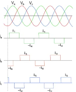
The thyristors in the Figure 2.1 are numbered according to the order in which they conduct, where at any given moment there are two thyristors conducting. For instance, when the line voltage, Vac, is positive then switches 1 and 2 conduct the DC current. This is followed by commutation of the current from switch 1 to switch 3, and so on. The phase voltage and current waveforms are seen in Figure 2.2.
𝐼𝑠,𝑊𝑌𝐸 =2√3𝜋 𝐼𝑑𝑐 [cos 𝜔𝑡 −
1
5cos 5𝜔𝑡 +
1
7cos 7𝜔𝑡
− 1
11cos 11𝜔𝑡 +
1
13cos 13𝜔𝑡 − ⋯ ] (1)
The magnitude of the harmonics of the fundamental are scaled by a factor of 1/n where n is the harmonic number. This is the ideal case for a wye connected converter.
The current for a delta connected converter is described by a slightly different equation where the signs of the harmonic terms change due to the phase lag/lead of the delta connected converter voltage with respect to the primary voltage.
𝐼𝑠,𝐷𝐸𝐿 = 2√3
𝜋 𝐼𝑑𝑐 [cos 𝜔𝑡 + 1
5cos 5𝜔𝑡 − 1
7cos 7𝜔𝑡
− 1
11cos 11𝜔𝑡 +
1
13cos 13𝜔𝑡 − ⋯ ] (2)
The observed harmonic current magnitude of a HVDC converter for a practical case is generally lower because of the impedance presented by the commutating reactance of the line. The detailed operation of the LCC will be investigated in Chapter 3.
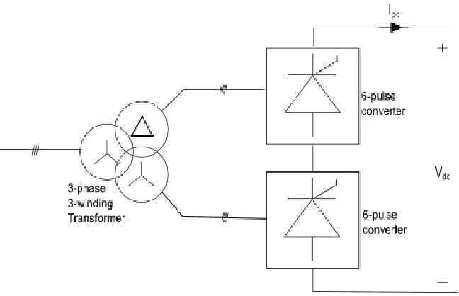
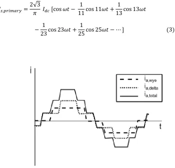
The modern HVDC station has a 12-pulse converter which consists of two 6-pulse converters, one connected to a Y-Y converter transformer and the other connected to a Y-Δ transformer. As is seen from (1) and (2) the signs of some of the harmonic terms of the wye connected converter are the opposite of the delta connected converter. Thus some of the harmonics are cancelled out by using a 12 pulse converter with careful design of the transformer reactance and synchronized firing pulse generation.
𝐼𝑠,𝑝𝑟𝑖𝑚𝑎𝑟𝑦 =2√3
𝜋 𝐼𝑑𝑐 [cos 𝜔𝑡 − 1
11cos 11𝜔𝑡 +
1
13cos 13𝜔𝑡
− 1
23cos 23𝜔𝑡 +
1
25cos 25𝜔𝑡 − ⋯ ] (3)
In short, for a n-pulse converter the order of harmonics, h, that is introduced into the AC system is
ℎ = 𝑘𝑛 ± 1 (4)
𝑤ℎ𝑒𝑟𝑒 𝑘 𝑖𝑠 𝑎 𝑝𝑜𝑠𝑖𝑡𝑖𝑣𝑒 𝑖𝑛𝑡𝑒𝑔𝑒𝑟
Thus, the lower order harmonics can be eliminated by using higher pulse converters. However, HVDC power transmission studies have shown that pulse numbers higher than 12 are not economical due to added complexities of the system [3].
A small magnitude of non-characteristic harmonics can also be introduced into the network due to firing angle errors and unbalances in the converter transformer reactance and the supply voltage. The phase mismatch on the AC side can generate odd harmonics while the firing angle error of the converters can also create even harmonics. These harmonics are usually neglected in harmonic studies since they have very low values.
Any nonlinear device such as a generator or power transformer will create harmonics in the ac network. Loads on the distribution network also add to the harmonic content of the grid. For this reason, the grid cannot be considered to be ideal when designing harmonic filters for converter stations.
2.3Effects of Harmonic Distortion
a. Interference with telephone lines – It is common practice for telephone lines to utilize the same infrastructure as transmission lines. If there are harmonics in the ac network these can interact with the adjacent communication lines and cause
interference.
b. Over-loading of capacitors – Fixed capacitors are used to improve the voltage profile of the line and also provide reactive power to the HVDC converter. If there is any resonance with the converter system at a higher frequency then the amount of harmonic current into the capacitor can amplify and cause over-loading. Even without overloading, the harmonic currents can increase the stress on the capacitor and result in a shortened capacitor life.
c. Equipment malfunction – In a similar way that the harmonics harm capacitors, other grid connected equipment can also be harmed due to increased heating. All rotating machinery heat up due to iron and copper losses at harmonic frequencies reducing the efficiency and also the torque produced. Similarly, copper losses and stray flux losses result due to harmonic currents in transformers.
2.4Harmonic Filters
It is apparent from the previous section that harmonic distortion in the AC network is very harmful and has to be eliminated. One way of filtering the harmonics is providing the high frequency currents a low impedance path using the combination of capacitors, inductors and resistors. These types of filters are called passive filters since they are comprised of passive elements. In addition to sinking the harmonic currents, these can also be used to provide reactive power support to the HVDC converter. A variety of filters can be employed specific to the need of filtering at the particular converter station. A short review of a few basic filters is presented in this section.
2.4.1 Single tuned filter
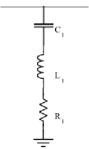
A single tuned or band pass filter is the most basic passive filter topology which consists of a reactor connected to a capacitor bank. A resistor may be added in series (usually it is just the loss of the inductor) to provide damping at the tuned frequency and lower the quality factor. In designing a single tuned filter, the value of the capacitance, C, is chosen depending on the amount of reactive power support expected. The inductance, L, can then be chosen so that the impedance of the branch is tuned to a minimum at the desired frequency using the equation
𝜔𝑛 = 1
√𝐿𝐶 (5)
𝜔𝑛 = 2𝜋𝑓0𝑛 (6)
If a certain quality factor, Q, is desired then the resistance, R, value can be chosen
𝑄 =𝜔𝑛𝐿
𝑅 (7)
so that the filter bandwidth increases and its performance around the tuned frequency is improved.
Figure 2.5: Single tuned or Band Pass Filter
Figure 2.6: Bode plot of single tuned filter
2.4.2 Double tuned filter
Figure 2.7: Double tuned filter
The performance of a double tuned filter can also suffer due to detuning and the complexity of the connections is increased when compared to single tuned filters.
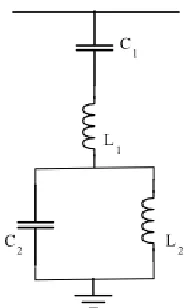
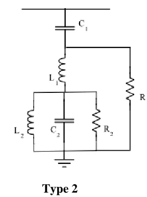
2.4.3 Damped double tuned filter
The double tuned filter can be modified to filter higher order harmonics and also improve the bandwidth at the tuned frequencies by using damping resistors. Two variations of damped double tuned filters are seen below with their impedance characteristics.
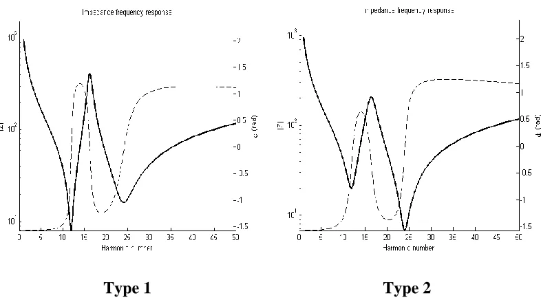
Type 1 Type 2 Figure 2.9: Damped double tuned filter
Type 1 Type 2 Figure 2.10: Bode plots of the damped double tuned filter
2.5Harmonic Standards
The objective of the AC filter design is to limit the harmonic currents in the grid so as to meet certain standards put forth by the utility. The IEEE has its own harmonic
performance specification that specifies the maximum allowable voltage and current
distortion in the AC network at the HVDC converter station. These guidelines also vary with a particular project depending upon the customer needs. These include limits for harmonic voltage distortion and telephone interference. An overview of the commonly accepted performance guidelines is given below.
2.5.1 Voltage Distortion
metrics to quantify the distortion in the grid among which the individual harmonic distortion (D) and the total harmonic distortion (THD) are most common among utilities. The
individual harmonic distortion is a measure of the voltage content at the point of common coupling (PCC) of each harmonic frequency. For each harmonic, n, this is calculated by
𝐷𝑛 = 𝑉𝑛
𝑉1 ∗ 100% (8)
where V1 is the fundamental frequency line to neutral voltage (RMS).
The THD index corresponds to the power of the harmonics and is therefore more closely related to the severity of the disturbance in terms of heating effects [5]. The formula for computing the THD is
𝑇𝐻𝐷 = √Σ𝑛=2𝑁 𝐷
𝑛2 (9)
where the maximum frequency order, N, is generally set to 50 as the magnitude of the injected harmonics from the HVDC converter is sufficiently diminished at higher
frequencies. Typically, the individual voltage distortion is to be kept under 1% and the THD is regulated between 1% and 4% depending on the system size.
2.5.2 Telephone Interference
telephone interference at the PCC. The first one is a measure of the voltage telephone interference (VTIF) and the other is based on the harmonic currents (IT).
𝑉𝑇𝐼𝐹 =√Σ𝑛=1
𝑁 (𝑉
𝑛𝑊𝑓𝑛) 2
𝑉1 (10)
𝐼𝑇 = √Σ𝑛=1𝑁 (𝐼 𝑛𝑊𝑓𝑛)
2
(11)
𝑘𝐼𝑇 = 𝐼𝑇
1000 (12)
where Vn and In are the harmonic voltage and current, and Wfn is the harmonic coupling factor.
Figure 2.11: Psophometric weighting factor (Wfn)
Some of the factors that are considered when defining the IT and VTIF boundaries are the density of telephone lines close to the ac network, the length and average separation from the AC lines, the type of the communication line and also the structure of the AC grid network. For the VTIF, the range between 25 and 50 is normally considered permissible while the kIT should be kept below 100 at the minimum.
The IEEE 519 Harmonic Standard for voltage distortion [6] is shown in Table 1.
Table 1: IEEE 519 Harmonic Standard for Voltage Distortion Harmonic Voltage Distortion in % at PCC
System voltage 2.3 – 69 kV 69 – 138 kV >138 kV
Dn 3.0 1.5 1.0
The current distortion standards vary as well depending on the short-circuit ratio (SCR) and can be looked up in [6].
2.6Harmonic Performance Analysis
In order to meet the harmonic performance specifications stated in the previous section it is important to conduct a system study and analyze the interaction of the grid and the filters. This analysis can be done in the time domain using real time digital simulation techniques and also in the frequency domain by creating harmonic models for the entire system. A basic frequency domain analysis technique that serves as a good starting point is the single frequency study of the system where the HVDC converter is treated as a harmonic current source and the small signal analysis of the circuit comprising of the harmonic
impedances of the grid and filters is done to calculate harmonic voltages and currents at the PCC. This method does not capture the harmonic interaction between the AC and the DC sides.
Here, Zsn is the system harmonic impedance and Zfn is the filter harmonic impedance while the converter current is denoted by Icn.
The time domain simulations can give more accurate data that can be recorded and analyzed in the frequency domain to measure the desired characteristics. In the time domain, the actual load flow analysis and the interaction in the power system is calculated in detail which makes the results more meaningful. However, a detailed model of the system is necessary to get good results. Software tools such as PSCAD are usually accepted for power system simulations.
2.6.1 System Impedance Modeling
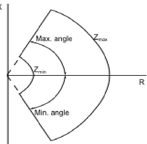
perimeter of the figure can be tested during the filter design process. The general sector model (Figure 2.13) is one of the methods of encompassing the impedance loci of the AC network. This is a worst case analysis which allows for a comprehensive design of filters. But this process could lead to over-design, in turn, increasing the cost and size of the harmonic filters. An alternative is to use an equivalent circuit that depicts the nature of the grid for most operating conditions by maintaining a constant impedance angle over the lower frequency range [8]. The CIGRE benchmark for a weak grid uses a simple voltage source behind an impedance of a resistive and reactive element with a SCR of 2.5 at 84degrees.
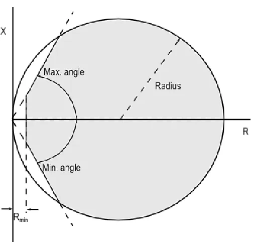
For the preliminary frequency domain study, the general circle method (Figure 2.14) was used to identify possible conditions of resonance between the filters and the grid. There are three parameters that define the area of interest in the general circle model.
a. Radius – The radius of the circle defines the maximum possible magnitude of the AC network impedance and forms the perimeter of the figure.
b. Rmin – This is the least possible resistance value of the grid. For any given condition, the resistance value cannot be lower than the minimum value given by Rmin.
c. Maximum angle – This is the largest possible X/R ratio of the grid. Together with the Rmin value, this makes the model a little more realistic and avoids overdesign to some extent.
By testing the filter impedance with the values on the perimeter of this figure it can be ensured that all values within the circle will also meet the desired harmonic performance specifications.
2.7System Resonance Issues
Once the filter is designed based on the harmonic filtering and reactive power
requirement, its impedance frequency characteristic can be created. The impedance model of the grid and filters is used to calculate the voltage and current values in the frequency
CHAPTER 3
HVDC System Design
In this chapter, the design process of the entire HVDC system is covered including the passive filters and the transformer. This forms the test system for the identification of the system resonance problem and further, the design of the Hybrid Active Filter to mitigate this situation.
3.1System specifications
There are various aspects of the HVDC system design process that begin with the specification of the AC system and the rating of the HVDC converter. According to the output requirements, the LCC operating point is chosen to design the parameters for the converter as well as the transformer. The filter design process involves identifying the harmonics created by the converter and then designing filters for those harmonics by following the harmonic performance analysis process described in the previous chapter. The specifications for the HVDC system are tabulated below.
Table 2: HVDC system specifications AC network
Voltage 345 kV (l-l, RMS)
Frequency 60 Hz
SCR 2.5
DC network
Power 500 MW
Voltage 250 kV
3.2LCC Design
relationship to the input AC voltage, firing angle and overlap angle that are the result of that study.
Figure 3.2: LCC circuit model
At any given instant, one thyristor of the upper commutation group (1, 3, 5) and one of the lower group (2, 4, 6) are conducting. Thus, the output DC voltage at any instant is one of the six possible line to line voltage combinations. The firing angle, α, controls the instant
Figure 3.3: Ideal LCC voltage and current waveforms
The resulting equation from [1] for the DC voltage is
𝑉𝑑𝑐= 𝑉𝑑𝑖𝑜cos 𝛼 (13)
𝑉𝑑𝑖𝑜 = 3√3𝜋 𝑉𝑚 (14)
where Vm is the magnitude of the input phase voltage.
valve to another. This is called the commutation period and quantified by the overlap angle, μ. The operation of the LCC during the commutation period is seen in Figure 3.4.
Figure 3.4: LCC circuit operation during commutation period
The effect of this commutation period is that the DC voltage is reduced due to the voltage drop across the line reactance. This drop is directly proportional to the DC current and the inductance of the commutating reactance.
Δ𝑉𝑑𝑐 =
3
𝜋𝜔𝐿𝑐𝐼𝑑𝑐 (15)
The resulting voltage is then captured by the presence of the overlap angle in
𝑉𝑑𝑐 = 𝑉𝑑𝑖𝑜cos(𝛼) + cos(𝛼 + 𝜇)
The reactive power consumed by the HVDC converter due to the phase delay between the current and voltage waveforms is given by
𝑄𝐿= 𝑃𝑑𝑐tan 𝜃 (17)
where cos θ ≈ Vdc/Vdio and Pdc = VdcIdc can be substituted in (17) to get
𝑄𝐿 = 𝑉𝑑𝑐𝐼𝑑𝑐√(
𝑉𝑑𝑖𝑜 𝑉𝑑𝑐)
2
− 1 (18)
Using these equations, the commutation reactance and required input AC voltage can be calculated to get the required output DC voltage. However, the input AC voltage and the commutation reactance are both defined by the transformer turns ratio if the per unit leakage reactance of the transformer has already been specified. Thus, the design process becomes iterative with the inclusion of the turns ratio of the transformer. A simple algorithm can be written to solve for the parameters that would give the desired results. A script was written in MATLAB for this process.
3.3Transformer Design
The transformer was specified to have a per unit leakage reactance of 12%. The transformer turns ratio is designed so that the required input voltage magnitude is available at the converter terminals so that it can function at the designed operating point.
As mentioned in the previous section, a MATLAB script was written to run an iterative design process to calculate the necessary turns ratio that fulfilled the condition of providing enough input voltage despite the voltage drop across the commutation reactance. The value of this reactance also depends on the turns ratio.
3.4Phase Locked Loop
The voltage at the PCC is detected and a PLL circuit is used to track the phase of the voltage waveform. While using the PLL it is important to determine the order of the valve firing and extract the phase so that the voltage signals are aligned with the respective switches. The firing pattern and the respective positive line voltages are shown in Table 3.
Table 3: Thyristor valve firing pattern Positive line voltage Valve number
Vac 1
Vbc 2
Vba 3
Vca 4
Vcb 5
Vab 6
Thus, the PLL is controlled so that the phase output is aligned with the line voltage, Vac, and the firing pulses are generated for the pattern listed in Table 3. The delta connected converter voltage has a phase lag of 30 degrees so the firing pulses must be shifted by 30 degrees to synchronize with the wye connected converter.
Figure 3.6: PLL control diagram
Here the term, ω1, is the fundamental angular frequency added to specify the system
frequency. The PI regulator sets the phase output to minimize the error and in the process controls the quadrature axis voltage to zero. The integrator wraps the values back to zero once it reaches 2π to keep the phase output between 0 and 2π. This serves as the feedback
transformation angle to get the q axis synchronous reference frame value.
3.5Initial Design Results
For the purpose of harmonic filter design, it is useful to analyze the worst case of harmonic generation by the HVDC converter. In HVDC converters used for power
for the worst case. The results of the design process for the LCC and transformer parameters were used to create a time domain simulation model in PSCAD. The grid was assumed to be an ideal voltage source to test the derived values. The simulation results are documented in this section that show the operation of the converter to supply the rated power at the rated DC voltage.
Figure 3.7: LCC direct voltage output
The results validate the design process and the parameters used for the HVDC system. However, without any filtering the grid supplies all the harmonic current that is required by the HVDC converter.
Figure 3.9: Source current for one phase
The phase current of the grid has very large amounts of harmonic current as can be seen in Figure 3.9 and Figure 3.10. The 12-pulse current waveform with the slope of the commutation period can be seen in Figure 3.9.
3.6Passive Filter Design
As can be seen from the harmonic content in the source current, it is important to design passive filters that will sink the major harmonics {11th, 13th, 23rd, and 25th} and also provide some damping for the higher order harmonics. Considering the need for multiple harmonic filtering and also a high pass characteristic, the damped double tuned filter is a good candidate for the filtering. The filter must be tuned to remove the major harmonics from the grid. The damped double tuned filter also has a good bandwidth around the tuned
Figure 3.11: Damped double tuned filter
In creating a double tuned filter, the challenge is to choose values for the passive elements based on the reactive power requirement, tuning frequencies and damping resistors while ensuring that the performance matches the requirements. Each of these control
parameters has a trade-off which makes the design iterative. The high voltage capacitor, C1, has to be chosen to meet the reactive power requirements of the converter. Once this has been selected, the conventional double tuned filter design method is followed to select the values for the remaining reactive elements. The following equations were derived from the design process in [10] and [11].
𝐶1 = −
𝑄𝐿
𝑉𝑠2(
𝜔𝑓 𝜔𝑠2−
1
𝜔𝑓+ 𝜔𝑓
𝜔12 + 𝜔
22− 𝜔𝑠2
𝜔𝑠2(𝜔
𝑝2− 𝜔𝑓2)
) (19)
𝐿1 = 1
𝜔𝑠2𝐶
𝐶2 = 𝐶1 𝜔12+ 𝜔
22− 𝜔𝑝2
𝜔𝑠2(𝜔
𝑝2− 𝜔𝑓2)
− 1
(21)
𝐿2 =
1
𝜔𝑝2𝐶2 (22)
𝜔𝑝𝜔𝑠 = 𝜔1𝜔2 (23)
where ω1 and ω2 are the tuned frequencies, ωs is the series resonance frequency of the circuit comprising L1 and C1, and ωp is the parallel resonance frequency of the circuit
comprising L2 and C2.
The parallel resonance frequency should be chosen to be between the tuned
Table 4: Designed filter parameters Passive element Value
C1 2.7012 μF
L1 8.344 mH
R1 400 Ω
C2 5.9332 μF
L2 4.463 mH
R2 400 Ω
Figure 3.12: Filter impedance frequency response
3.7PSCAD Results
time domain simulation and the filter also provided reactive power compensation to the converter. Some of the reactive power support was provided by a capacitor bank which also drained some higher order harmonics due to its low impedance at high frequencies. The resulting three phase current waveforms for the system are seen in Figure 3.13 and their harmonic current magnitude plot is seen in Figure 3.14.
Figure 3.14: System harmonic current magnitude
Figure 3.16: Individual harmonic voltage distortion
Figure 3.17: Harmonic performance specifications
The designed filter is able to meet the harmonic performance requirements and also provide the reactive power support to the HVDC converter. However, as discussed in
3.8System Resonance Analysis
In order to identify possible resonant conditions of the system, a frequency domain analysis was done using the harmonic system model introduced in Chapter 2. The converter was modeled as a harmonic current source and the general circle model was used for the grid. The harmonic values for the grid conditions were obtained from a consultant at General Electric. The designed filter was tested with all possible values on the perimeter of the grid impedance circle at each frequency to find the worst case resonance.
Figure 3.18: General circle model for a single harmonic frequency
The algorithm for the analysis found the worst cases of resonance at each harmonic frequency by solving for the voltage and current at the PCC for the combination of the filter impedance at that frequency with all possible grid impedance values as defined by the general circle. This is an extreme analysis since a grid condition that causes resonance at every harmonic is not realistic. However, it confirms the problem of resonance and stresses the need for prudent filter design as well as alternate solutions to filtering.
The bar graph in Figure 3.20 gives an indication of how the harmonic performance suffers during this resonance case. The normalized value in the figure is the multiple of the allowable limit.
To get a more realistic view of the effects of grid resonance, a grid impedance that caused resonance at the 11th harmonic with the filters was identified using the MATLAB analysis and was used in a time domain simulation.
The impedance of the resonant grid from the MATLAB analysis was modeled after the AC network voltage source and a simulation was run to verify if the harmonic
performance of the filters degraded because of resonance. The results showing the effect of the system resonance on the grid current are seen in Figure 3.21.
Figure 3.22: Harmonic magnitude plot of the currents in Figure 3.21
The large values of the 11th and 13th harmonic currents are seen from the
Figure 3.23: Harmonic performance indices during system resonance
CHAPTER 4
Active Filters
The inability of passive filters to guarantee harmonic filtering due to problems such as resonance with the grid and detuning has led to the use of active filters at non-linear loads. Passive filters also occupy a large area and have a significant cost. Besides, the design process for a passive filter is very complicated and relies on accurate data of the network conditions. The fact that a system evolves over time and is bound to change adds to the intricacy of passive filter design. This makes the active filter an option to consider for filtering harmonics for HVDC converters.
4.1Background
An active filter cancels the harmonic content in the load by injecting harmonic currents with the same magnitude but opposite phase. The active filter first detects the amplitude and phase of the AC current harmonics and then creates the appropriate harmonic voltage to negate those harmonics. This is achieved by using an IGBT controlled VSC. The converter uses power from the AC system to function as an active harmonic source. Since the converter appears as a voltage source to the system, there is no interaction with the rest of the system unlike the passive filters.
improvement in recent years, the IGBT is suited for low to medium voltage applications since it cannot block very high voltages. For this reason, the use of active filters for HVDC converters is limited.
4.2Voltage Source Converters
The basic DC-DC converter principles form the base for the operation of the VSC. The main advantage of the IGBT is that it can be turned on or off with a gate signal whereas a thyristor is dependent on negative line voltage for turning off. Hence, it is possible to have complete control over the converter current which gives the VSC the ability to not only create any current profile but also to supply leading or lagging current which allows for control over the reactive power.
The VSC is termed so because it has a fixed DC voltage for both rectifier and inverter modes of operation. The thyristor based LCC has a fixed current polarity while the VSC can conduct current in both directions while maintaining a fixed voltage polarity.
The modeling of a VSC for the purpose of designing controls is investigated in the following section. A complete analysis involves the derivation of the converter transfer functions. These define the operation of the converter and are taken as the plant for which compensators are designed.
4.2.1 System Representation
The analysis of the converter operation is done to get equations to describe the system behavior and also create transfer functions that can be utilized with the control theory to design voltage and current regulators.
Figure 4.2: AC side VSC circuit model
link voltage. The analysis presented considers phase voltages and the loss in the inductor is modeled as a resistor, R. An in-depth derivation of the system equations can be found in [13]. Following the rules of Kirchhoff’s circuit laws we get
𝑣𝑠,𝑎𝑏𝑐 = 𝑣𝑐,𝑎𝑏𝑐+ 𝐿𝑠
𝑑𝑖𝑎𝑏𝑐
𝑑𝑡 + 𝑅𝑖𝑎𝑏𝑐 (24)
The p-q theory introduced in [14] allows instantaneous compensation of reactive power in three phase circuits and for non-linear loads. The three phase equations are transformed to the rotating reference frame according to this theory. The use of the
synchronous dq reference frame allows decoupled control of active and reactive power flow [12]. The basis for this transformation is found in Appendix A. The convention chosen for the dq transformation is that the direct axis controls real power and the quadrature axis
controls the reactive power. (Eq. 24) is transformed to the synchronous reference frame to get
𝑣𝑠,𝑑 = 𝑣𝑐,𝑑+ 𝐿
𝑑𝑖𝑑
𝑑𝑡 − 𝜔𝐿𝑠𝑖𝑞+ 𝑅𝑖𝑑 (25)
𝑣𝑠,𝑞 = 𝑣𝑐,𝑞+ 𝐿𝑑𝑖𝑞
𝑑𝑡 + 𝜔𝐿𝑠𝑖𝑑 + 𝑅𝑖𝑞 (26)
The objective of deriving these equations is to control the converter voltage by creating a current reference. Hence, the system voltage and cross-coupling inputs to this equation are compensated through feed-forward, and the Laplace transformation of (26) gives a relationship between the current and the converter voltage.
𝑖𝑑/𝑞
𝑣𝑐𝑑/𝑞 = − 1
This transfer function is used as the plant in control theory and a current compensator is designed to regulate the converter output voltage. The negative sign of the transfer function comes from the convention of measuring current going into the converter as positive. If the opposite convention is used then this sign will disappear.
For the DC link voltage control, the power balance theorem can be used to derive the equations for the DC side of the converter. Assuming no losses in the switches and the
inductor, the power from the AC system, Psrc, must equal the power delivered to the DC load, Pload.
𝑃𝑠𝑟𝑐 = 𝑃𝑙𝑜𝑎𝑑 (28)
From the IRP theory, we have
𝑃𝑠𝑟𝑐 =
3
2(𝑉𝑑𝐼𝑑 + 𝑉𝑞𝐼𝑞) (29)
and according to the chosen convention for the SRF, Iq = 0 since it does not contribute real power. Thus, we get
𝑃𝑠𝑟𝑐 = 3
2𝑉𝑑𝐼𝑑 (30)
and
𝑃𝑑𝑐 = 𝑉𝑑𝑐∗ 𝐼𝑑𝑐 (31)
where Vdc* is the reference DC voltage. Substituting (30) and (31) in (28) we can derive the equation for the DC link operation of the converter where
𝐼𝑑𝑐= 𝐶𝑑𝑉𝑑𝑐
3
2𝑉𝑑𝐼𝑑 = 𝑉𝑑𝑐∗ 𝐶 𝑑𝑉𝑑𝑐
𝑑𝑡 (33)
Here Vd is the direct axis voltage of the AC system to which the converter is connected and C is the DC link capacitance. Taking the Laplace transform and rearranging we get,
𝑣𝑑𝑐
𝑖𝑑 =
2 ∗ 𝑉𝑑𝑐 3 ∗ 𝑉𝑑
1
𝑠𝐶 (34)
This is the transfer function for which the voltage regulator will be designed that will output a current reference for the current regulator.
4.2.2 Control Design
The control objectives for a VSC can vary depending on the application of the converter. For power control a current reference can be generated by doing the required arithmetic to solve for the reference to the current regulator which will generate the necessary converter voltage to meet the power requirement. In the rectifier mode, the goal of a
Figure 4.3: Control diagram overview for DC link voltage control
The converter is modeled in the control diagram with the system transfer functions. The controller output signals, Vaf,d* and Vaf,q*, are then transformed back to three phase
signals and divided by 𝑉2
𝑑𝑐 to get the modulating signal for the sine-triangle PWM technique
Figure 4.4: Sine-triangle PWM generation
These pulses are supplied to the gates of the switches to control the converter operation. If instantaneous real or reactive power control is desired then another outer PQ control loop will create a current reference which can be added to the reference created by the DC link voltage regulator. A big challenge in control design is to design the gains of the current and voltage regulators. The next two sections present a summary of the design of PI controllers the details of which can be found in [14].
4.2.2.1Current Regulator
The current compensator controls the current going into the converter to regulate the converter voltage. The relationship between the current and the voltage of the converter was derived in the previous section to get the transfer function
𝑖𝑑/𝑞 𝑣𝑐𝑑/𝑞 = −
1 𝑠𝐿𝑠+ 𝑅
which is the plant for the control design model. This transfer function has a pole that must be cancelled using the zero of a PI compensator. The tuning of the proportional and integral gain by the technical optimum gain tuning method can be set as
The bandwidth of the regulator, ωbw, can be chosen depending on the switching frequency
and the feedback measurement delay. The MATLAB sisotool is also a valuable tool in designing the controller gains according exact response requirements.
Figure 4.5: Current regulators in the SRF
The simplicity and zero steady state error of the PI regulator in the SRF with the feed-forward terms make it a good choice for controlling the current.
4.2.2.2DC Link Voltage Regulator
the power balance theorem previously. In [14] a second order nonlinear relationship is derived to calculate the gains for the PI regulator.
Figure 4.6: Voltage control using PI regulator
The result from [14] for the frequency domain analysis used to derive the gains is
𝑉𝑑𝑐 𝑉𝑑𝑐∗ =
𝜔𝑛2
𝑠2+ 2𝜁𝜔
𝑛𝑠 + 𝜔𝑛2 (35)
𝐾𝑝 =
2𝜁𝜔𝑛𝐶𝑉𝑑𝑐∗
3 2 𝑉𝑚
𝐾𝑖 =
𝜔𝑛2𝐶𝑉 𝑑𝑐∗
3 2 𝑉𝑚
(36)
Where ωn stands for the natural undamped frequency and ζ stands for the damping factor.
With these gains the bandwidth of the regulator is given by
𝜔𝑏𝑤 = 𝜔𝑛√(1 − 2𝜁2) + √4𝜁4 − 4𝜁2+ 2 (37)
forms the reference to the direct current regulator. As a rule of thumb, the bandwidth of the outer loop DC link control can be around one sixth of the inner current controller bandwidth.
4.3Active Filter Topologies
Depending on the way the VSC is connected to the system the converter can operate as a series active filter or a shunt active filter. These are the two topologies of the pure active filter connected to a system that has a nonlinear load.
4.3.1 Series Active filter
In this filtering method, the active filter is tapped from a transformer connected in series with the ac line. The converter is controlled to inject voltages that cancel out the distortion present in the system. Thus the source voltage remains distortion free.
The problem with the series active filter is that all the fundamental current that flows through the transformer to the load has to go through the active filter as well which
significantly increases the rating of the filter. It is certainly not a feasible option for the high voltage and current ratings of HVDC. However, it can be used as a filtering solution for small and even medium voltage applications.
4.3.2 Shunt Active filter
In this configuration the active filter is connected to the PCC in parallel with the load. A step down transformer is needed to reduce the voltage at the converter. Similar to the series active filter, the shunt active filter detects the harmonics in the load current and injects the opposite phase current to eliminate any high frequency current from the source. Since the transformer is not connected in series with the line, the converter does not have to conduct all the fundamental current. However, because of the leakage reactance of the transformer and the high turns ratio required to sufficiently step down the voltage at the converter, a
Figure 4.8: Shunt active filter
The control for the converter can also be made to sense the harmonics in the source current and then cancel them out. One implementation of the control for an active filter is seen in Figure 4.8.
The low frequency component of the source current is removed to form the reference for the converter current control along with the reference created by the DC link voltage control. This way the converter voltage can be regulated to inject the required harmonics. However, as noted before, a lot of fundamental current can flow through the converter due to the transformer leakage reactance. Considering that the converter is connected to the PCC, there is also a reasonable fundamental voltage in spite of the step down transformer. This greatly increases the power flow through the converter and also the converter rating.
CHAPTER 5
Hybrid Active Filters
5.1HAF Review
Due to the rating problems of the pure active filter, it cannot be utilized for HVDC systems where the voltage and current ratings are extremely high. For this reason, various HAF topologies [20] have been proposed. The motivation for having a HAF is to reduce the rating of the active filter either by diverting the fundamental current away from the active filter and minimizing the fundamental voltage seen by the converter.
One implementation of a shunt connected hybrid active filter that improves the performance of single tuned passive filters from [21] is discussed here.
A passive branch is added in series with the shunt connected converter. The passive branch is tuned to provide a low impedance path at the tuned frequency allowing the converter to inject the required harmonics currents. However, the passive branch can be tuned to only one frequency which makes the active filter function limited to the filtering of a single frequency. It might be desirable to employ such HAF for the dominant harmonics as these filters provide the benefit of addressing variability around the tuned frequency as opposed to single tuned passive filters that also suffer from the effects of detuning and resonance. Another advantage is that the passive filter capacitor supports the fundamental voltage which reduces the voltage rating of the converter and the impedance to the
fundamental current is also high as the passive branch forms a band pass filter. The control of this converter is done in the SRF by rotating the three phase reference current at the
frequency of compensation to extract the harmonic reference.
5.2Proposed HAF Topology
The HAF discussed in the previous section is effective to improve the performance of a single tuned filter. However, it still requires multiple HAFs to address the dominant
harmonic currents as well as a high pass filter for the higher order harmonics. It was seen that the double tuned filter provided many advantages over the single tuned filter when
an active filter is connected to a shunt attached double tuned passive filter. This filter configuration allows active filtering of the dominant harmonics when needed.
Figure 5.2: Proposed HAF Topology
Some of the advantages of this topology are listed below –
b. Lower rating of active filter – The lower portion of the filter branch provides low impedance for the fundamental current so that the fundamental voltage across that segment of the passive filter is small. This reduces the voltage rating of the active filter which is connected in parallel with the lower branch and also requires a smaller turns ratio for the transformer. Also, the fundamental current is diverted through this passive branch which reduces the power rating of the active filter.
c. Reactive power support – The high voltage capacitor of the high pass branch of the passive filter supports all the fundamental voltage and also provides reactive power support to the HVDC converter.
d. Active filtering at dominant harmonics – The lower portion of the passive filter has a parallel resonance close to the 11th and 13th harmonics which enables the active filter to inject currents at those frequencies back into the grid through the high pass portion.
e. Resonant condition harmonic compensation – The active filter can share the load of the dominant harmonics which makes this HAF effective even if the passive filter and the grid create a resonance.
Hence, the hybrid active filter topology allows the voltage source converter to have a lower rating and provide the passive filter with filtering support. In case of detuning of the passive elements, the active filter can provide the necessary dominant harmonic
A major challenge with the proposed HAF is the design of the controls due to the
complexity of selecting two harmonic currents for compensation while maintain the DC link voltage which requires fundamental current. The control design process is investigated in the following section.
5.3Control Design
According to the HAF design, it is expected that the active filter provide compensation for the 11th and 13th harmonic currents which are the dominant currents injected by the HVDC converter while maintaining the DC link voltage. The SRF technique of harmonic selection employed in [23] is useful for compensation of a single frequency current. It transforms the three phase reference current by rotating at the frequency of compensation. However, this cannot be replicated for the proposed HAF because references generated for two distinct harmonics, by rotating at two different frequencies, cannot be added in the SRF to create a common reference current. Thus, the PR controller in [24] is implemented with this HAF.
5.3.1 PR Regulator Design
In [24] the PR regulator is developed in the stationary frame as an equivalent compensator to the PI regulator in the synchronous reference frame. This PR regulator can achieve zero steady state error without requiring complex transformations of a synchronous frame regulator. The ideal form of the PR controller is given by the transfer function
𝐺𝐴𝐶(𝑠) = 𝐾𝑝+ 𝐾𝑖 𝑠2+ 𝜔
Here the controller has unlimited gain at the natural undamped frequency, ωn. Thus, this can
be used to directly control the AC signal. However, the infinite gain could cause stability problems and due to the practical limitations of signal processing, a damped form of the resonant controller transfer function is used.
𝐺𝐴𝐶(𝑠) = 𝐾𝑝+
2𝐾𝑖𝜔𝑐𝑠 𝑠2+ 2𝜔
𝑐𝑠 + 𝜔𝑛2 (39)
𝑤ℎ𝑒𝑟𝑒 𝜔𝑐 = 𝜁𝜔𝑛
The damped frequency, ωc is the bandwidth around the natural frequency and can be controlled by the damping ration ζ. Even though the gain is finite at ωn, it is tuned to be large
enough to eliminate all steady state error. The controller bandwidth can be increased by introducing more damping.
5.3.2 PR Regulator in the stationary frame
In order to utilize the PR controller, the harmonic reference current must be extracted using a band pass filter with unity gain. The filter transfer function matches the resonant controller transfer function with the absence of the gain Ki. After the harmonic current extraction, the reference is transformed to the stationary αβ frame to control the AC signal, although the transformation is not required to utilize the PR controller. The advantage of converting to the stationary frame is that only two controllers are required, one for the α axis current and the other for the β axis current, whereas three controllers are required in the three
phase system.
The control was tested for a non-linear load in the form of a three phase diode rectifier which is connected to an AC system modeled as an ideal three phase voltage source (Figure 5.4). The converter is controlled to remove the 5th and 7th harmonics from the source current.
The results of using the PR regulator in the stationary frame to control the active filter current are seen in the plots in Figure 5.5.
Figure 5.5: a) Source current waveform without (on top) and with active filter, b) Harmonic magnitude without (left) and with active filter
Figure 5.6: Reference current tracking using PR regulator in stationary frame
However, the PR controller in the stationary frame requires a regulator for each harmonic that is to be compensated.
5.3.3 PR Regulator in the synchronous reference frame
The PR controller employed in the SRF is equivalent to the conventional PI controller implemented in the SRF, separately for the positive and negative sequences. For instance, a twelfth harmonic PR regulator can control both the eleventh and thirteenth harmonic
done for higher order harmonics, if needed, with the addition of a PR controller tuned at the 6th, 18th, 24th, 30th and so on.
When the SRF transformation is done the positive and negative sequence elements are accumulated at the zero sequence harmonic. For instance, the 5th harmonic negative sequence current and the 7th harmonic positive sequence current are rotating at the 6th harmonic relative to the frequency of rotation of the SRF. Thus, after the rotation, the 6th harmonic current can be extracted using a band pass filter to generate the reference for the PR controller in the SRF. The controller then regulates the AC signal to match the reference and the result is that both harmonics of concern are addressed. The results of the PR regulator for the test system of Figure 5.4 are shown below.
The current tracking using the PR regulator in the SRF is seen below and the results match the simulation in the previous section of a PR regulator in the stationary frame. Only one controller is required to compensate both harmonics in the SRF whereas the stationary frame needs a controller for each harmonic.
Figure 5.8: Reference current tracking using PR regulator in the synchronous frame
Figure 5.9: Overview of the control diagram for the active filter operation
Figure 5.10: Inner current control open and closed loop transfer function Bode plot
Figure 5.11: Outer voltage control open and closed loop transfer function Bode plot
Current control loop bode plots
Frequency (Hz) -40 -20 0 20 40 60 M a g n itu d e ( d B )
101 102 103 104 105
-135 -90 -45 0 P h a s e ( d e g ) Open-loop Closed-loop
100 101 102 103 104 105
-180 -135 -90 -45 0 P h a s e ( d e g )
Voltage control loop bode plots
5.4Hybrid Active Filter Implementation with HVDC system
CHAPTER 6
Results
The time domain simulation of the HAF connected to the HVDC system designed in Chapter 3 was done in PSCAD. The HAF performance was tested for the condition of system resonance that caused the passive filter to be ineffective as seen in the PSCAD results of Chapter 3.
6.1PSCAD Simulation Results
In this section, the current and voltage waveforms and the derived frequency domain results for the harmonic performance metrics have been documented.
The current waveform in Figure 6.2 shows the result of system resonance without the use of the HAF. This result is for a grid impedance value that is causing resonance at the 11th and 13th harmonics.
Figure 6.2: Grid current profile during system resonance without the HAF
The goal of the HAF is to remove these amplified current harmonics from the source. The results that follow are with the HAF implemented during the same system resonance condition at the dominant harmonics.
Figure 6.4: Grid current profile during system resonance with the HAF
It is clear from the difference in the Fourier spectrum plot in Figure 6.3 and Figure 6.5, that the 11th and 13th harmonic current magnitudes are greatly reduced in the grid current due to the operation of the HAF. The load current remains unchanged and the load current waveform and Fourier spectrum plot are seen in Figure 6.6 and Figure 6.7, respectively.
Figure 6.6: Transformer primary current waveform with HAF
The performance of the PR controller is seen in the tracking of the direct axis reference current by the regulator. The reference current is the sum of the DC link voltage controller as well as the harmonic reference extracted from the source. The active filter direct axis current is controlled by the PR regulator.
Figure 6.8: Direct axis current tracking performance of the PR regulator
Figure 6.9: Grid voltage waveform at the PCC
Figure 6.10: Fourier spectrum of the grid voltage at the PCC
The harmonic performance indices in the frequency domain are calculated dynamically during the simulation and are seen in the bar plots in Figure 6.11. The
Figure 6.11: Harmonic performance indices during system resonance with the HAF
It can be seen that the performance metrics established in Chapter 2 are met with the help of the HAF even when the passive filters are debilitated due to resonance with the grid
impedance.
Figure 6.12: DC link voltage step response
The overshoot is controlled by having a high damping factor to get a high phase margin. The DC link voltage tracking during harmonic compensation is seen in Figure 6.13.
The active filter rating is found to be less than 1% of the HVDC converter rating of 500 MW. As can be seen by the plot in Fig. 6.14, the active filter has a rating of less than 0.4 MVA during the worst case harmonic current compensation.
Figure 6.14: Active filter power during harmonic current compensation
For a condition where there is no system resonance and the passive filters are able to remove the harmonic currents, the rating of the active filter is reduced to a little more than 0.1% of the HVDC converter rating.
6.2RTDS Simulation Results
The entire HVDC system was also simulated in RTDS to confirm the PSCAD results. However, an average model of the VSC was used instead of the complete switching model due to limitations of the maximum switching frequency in RTDS.
Figure 6.16: HVDC system model in RTDS
Figure 6.17: HVDC converter output - a) DC current, b) DC Voltage
The results of the grid current and voltage without and then with the passive filters is seen in Figure 6.18 and Figure 6.19, respectively.
Figure 6.18: Grid current without passive filters (left) and with passive filters (right)
0 0.03333 0.06667 0.1 0.13333 0.16667 0.2 1.8 1.86667 1.93333 2 2.06667 2.13333 2.2 kA IDC
0 0.03333 0.06667 0.1 0.13333 0.16667 0.2 235 240 245 250 255 260 265 VDC
0.00759 0.01863 0.02968 0.04073 0.05178 0.06283 0.07387 -2 -1 0 1 2 kA ISA
Figure 6.19: Grid voltage without passive filters (left) and with passive filters (right)
The system resonance condition was then investigated by changing the impedance of the AC grid to cause resonance with the passive filters at the dominant harmonics. The waveform of the source current during this condition is seen in Figure 6.20.
Figure 6.20: Grid current profile during system resonance without the HAF in RTDS (left) and PSCAD (right)
0.05368 0.06385 0.07402 0.08419 0.09436 0.10453 0.11471 -400 -266.667 -133.333 0 133.333 266.667 400 VS1
0.05368 0.06385 0.07402 0.08419 0.09436 0.10453 0.11471 -400 -266.667 -133.333 0 133.333 266.667 400 VS1
And the grid current waveform with the application of the HAF average model is seen to improve due to the compensation of the harmonic currents by the active filter.
Figure 6.21: Grid current profile during system resonance with the HAF
The performance of the HAF directly after being turned on for harmonic current compensation is seen in Figure 6.22.
Figure 6.22: Grid current before and after turning on Active Filter
0.06835 0.07748 0.08661 0.09574 0.10487 0.114 0.12313
-2 -1 0 1 2 kA ISA