Design of OPAMP Based Applications using 120 nm
Technology
Gohil Dharmendra R.#1
, Mohd. Abuzer Khan
*2#
Electronics & Communication, R.G.P.V Bhopal L.K.C.T. Indore M.P. India
1
2
Abstract
-
This paper introduces a generalized method for simulating the various applications of operational amplifier generally termed as op-amps using TSpice. Now days engineering education is taught using simulation software. The usefulness of this SPICE software in learning various application of op-amp is enormous than proto typing practical laboratory. This PSPICE software’s which are important part of engineering education plays significant role in analyzing and simulating the various applications of op-amp such as summing, integrator and comparator. We will present some designing, analysis and simulation of specific applications of op-amp using this software’s in detail which plays a vital role in various field of engineering.Keywords
— Nmos, Pmos
Operational amplifier, TSpice, SPICE, software.Introduction
Operational amplifier in present-day is the most widely used electronics device in field of electronic systems such as communications systems, medical electronics, instrumentation, signal processing and performing many mathematical operations such as addition, subtraction, multiplication, integration and differentiations etc. It consists of various stages namely input stage, intermediate stage gain, level shifting stage and output stage and is fabricated as an integrated circuit. The symbol of typical op-amp is shown in fig.1.
Fig1. Circuit symbol of op-amps
It has two input terminal named inverting V- and non inverting terminal V+ and one output terminal Vout. Vs+ and Vs- are power supply terminal. The ideal operational amplifier characteristics are:
1. Infinite input impedance 2. Zero output impedance 3. Voltage gain is infinite 4. Bandwidth is also infinite 5. Slew rate is infinite
6. Common mode rejection ratio is infinite 7. input Offset voltage is zero
The IC 741 is widely used general purpose op-amp whose circuit symbol is shown in fig 1.The Op-amp can be used in two configurations namely Open loop configuration and closed loop configuration. The open loop configuration is one in which no feedback in any form is fed to the input from the output whereas closed loop configuration is in which a fraction of output is fed back to input. A few limitations of open loop configurations are: 1. clipping of output waveform may occur if output voltage exceeds saturation voltage of op-amp. 2. Open loop gain is not constant 3. Bandwidth is negligibly small. That why this Configuration is not suitable for AC applications but it finds use in non linear applications such comparators, square wave generator and astable multivibrator. The closed loop configurations finds its utilization in linear applications such adder, transconductance amplifier, instrumentation amplifier, integrator, differentiator, log and antilog amplifier.
II. VARIOUS APPLICATIONS OF OP-AMP
1.
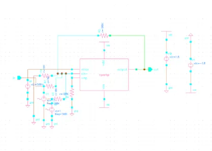
Designing of Comparator
delay and input signal range (5).Comparators are
classified
depending
upon
there
nature,
functionality and inputs. Like voltage and current
comparators, continuous and discrete time, etc.
Some of the basic application of comparators is
analog-to-digital conversion, function generator,
signal detection and neural networks etc.
Figure 2: Schematic Design of latch-Comparator
The latch- comparator is simulated using a
sinusoidal input signal to the differential pair in its
one terminal and making the other ground, two
non-overlapping and complementary clock signals
are applied, which helps the comparator to
improves its speed, as well as the sampling
frequency of the quantizer, 3 shows the transient
analysis of the latched comparator. Here the analog
input signal is compared against last sample signal
to see if it is higher than the reference or not. If it is
larger than the output is increased else decreased.
Figure 3: Simulated waveform of Comparator
2.
Designing of Summing Amplifier
The summing amplifier is a very flexible circuit
based on the standard operational amplifier,
which can be used for combining multiple
inputs. It has a single input voltage applied to the
inverting input terminal. If more resistors are
added to the input equal to the input resistor, we
end up with another operational amplifier called
as summing amplifier. Figure 4 shows the circuit
of a summing amplifier
Figuure 5:
Simulation result of summing amplifier
3.
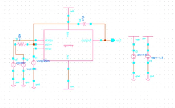
Designing of Integrator
The integrator is designed using a two stage
Op-Amp,
in
cadence
0.12um
CMOS
technology and is connected with a feed- back
capacitor which helps in charging of the input
voltage to give a integrated output. It is given a
sinusoidal input signal from the summing
amplifier whose output is the sum of the input
and the feed-back signal and gives ramp output
corresponding to a given sinusoidal input. The
below 6 shows the structure of an integrator
circuit and 7 gives the simulation result of the
integrator.
Figure 6
schematic of Integrator
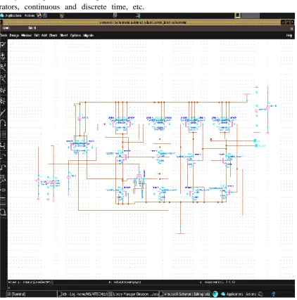
This paper mainly discusses the various applications of 741 operation amplifier and their simulations using TSpice software. We can design, simulate and verify any of applications with required parameters. Because of graphical facilities of TSpice, it is useful in enhancing the understanding of various applications of op-amps. We can also use different spice software like LT spice, Top Spice and Spice Opus for better understanding of various applications and compare the results with theoretically calculated result.
REFERENCES:
[1] Boylestad R., L. Nashelsky, 1992. Electronics Devices and Circuit Theory, Prentice-Hall Inc.
[2] PSPICE A/D online manual
[3] National Semiconductor Company, National Operational Amplifier databook, 1995 [4] Rashid M.H. Microelectronics Circuit Analysis and Design, PWS Publishing Co, 1999