Simulation &Analysis of Z Source Inverter Using
Different Modulation Control Techniques
Sandeep Kumar, Er. Vinay Kumar Tripathi2
PG Student [PE], Dept. of EE, SHIATS, Allahabad, UP, India1
Assistant Professor, Dept. of EE, SHIATS, Allahabad, UP, India2
ABSTRACT:The Z-source converter (ZSC) is an alternative power conversion topology that can both buck and boost the input voltage using passive components. It uses an unique LC impedance network for coupling the converter main circuit to the power source, which provides a way of boosting the input voltage, a condition that cannot be obtained in the traditional inverters. It also allows the use of the shoot-through switching state, which eliminates the need for dead times that are used in the traditional inverters to avoid the risk of damaging the inverter circuit. The selection of high modulation index and shoot-through duty ratio can reduce the inverter’s dc link voltage overshoot and increasing power delivery capacity of the inverter. Also by controlling the shoot-through duty cycle of IGBTs in inverter system, the line harmonics reduces, improves power factor, and extends output voltage range. This paper presents the analysis Maximum Boost and the Maximum Constant Boost control techniques in Z-source inverters. The voltage gain versus modulation index from simulation result is compared. Further detailed analysis of total harmonics distortion of output voltage at different modulation indexes for different boosting techniques of a Z-source inverter are performed by MATLAB based simulation.
KEYWORDS: Z-source converter, Maximum Constant Boost control techniques, Total Harmonic Distortion.
I.INTRODUCTION
To overcome the limitations and problems of the traditional or conventional source converters, an impedance-source (or impedance-fed) power converter (that can be abbreviated as ZSC) is introduced. Figure-1 depicts the general structure of ZSC. It employs a special impedance network (or circuit) that connect the voltage source converter and current converter main circuit to the power source, load, or another converter, for providing special features that cannot be seen in the conventional voltage source and current source converters where a capacitor and inductor are used, respectively [7]. ZSC structure using the series combination of switching devices like IGBT and diode is depicted in Figure-1, The Z source concept is applicable on all dc-to-ac, ac-to-dc, ac-to-ac, and dc-to-dc power conversion. The configuration of a ZSI consists of the following components:
1. Two Inductors 2. Two Capacitors 3. DC source
4. Inverter or Converter 5. Load or Converter
Figure-1.1 depicts the general structure of the ZSI. A ZSI structure uses the series combination of IGBT and diode. It overcomes all the theoretical barriers and limitations of the traditional VSI and CSI and gives rise to a new power conversion concept. Figure-1 depicts a two-port network that consists of two split-inductors L1, L2 and capacitors C1,C2 connected in X shape to provide an impedance source (Z-source) coupling the converter (or inverter) to the dc source, load, or another converter [7]. The dc source/or load may be either a voltage or a current source/or load. Hence, the dc source can be a battery, diode rectifier, thyristor converter, fuel cell, an inductor, a capacitor, or any combination of these. Series combination of IGBTs and diode are used as switches in the converter circuit. The inductance L1and L2 can be provided by a split inductor or two separate inductors.
II.
Z SOURCE INVERTERZSI can be used for dc-to-ac, ac-to-dc, dc-to-dc or ac-to-ac power conversion. It employs a special impedance network to combine the converter main circuit to the dc power supply. ZSI structure is already shown in Figure-1. The two port network consists of split-inductors L1 and L2 and capacitors C1 and C2 connected in X-shape [10]. Unlike traditional inverters [2] it provides special buck-boost feature to inverter by utilizing the shoot-through zero states by gating on both upper and lower switches of a phase leg. Therefore the ZSI can boost voltage and produce a required output voltage that is greater than the available dc bus voltage. In addition to this, the reliability of the inverter is greatly improved because the shoot through due to miss gating can now no longer destroy the circuit. Thus it gives a low-cost, reliable, and high efficiency single stage structure for buck and boost power conversion.
III. OPERATING PRINCIPLE OF ZSI
The special feature of the ZSI is that its output ac voltage can be any value between zero and infinity. That is, the ZSI is a buck–boost inverter that has a wide obtainable voltage area. The traditional VSIs and CSIs do not provide such characteristics. Unlike the traditional or conventional three-phase VSI that has eight switching states the ZSI bridge has nine permissible switching states (vectors).
The six active vectors when the dc voltage is connected across the load.
Two zero vectors when the load terminals are shorted through either the upper or lower three devices, respectively. One more zero state (or vector) when the load terminals are shorted through both the upper and lower devices of
any one of the phase leg (i.e., both devices are gated on), any two phase legs, or all three phase legs.
This shoot-through zero state (or vector) is not present in the traditional VSI, otherwise shoot-through would occur. This extra zero state (vector) is called the shoot through zero state (or vector). This shoot-through zero state can be produced in seven different ways:
Shoot-through via any one phase leg Combinations of any two phase legs All three phase legs
The Z-source network has accomplished the shoot-through zero state. This shoot-through zero state gives the special buck-boost feature to the inverter. Figure-3.1 depicts the equivalent circuit of the ZSI when seen from the dc link [9]. The inverter bridge is similar to a short circuit when the inverter bridge is in the shoot-through zero state, as depicted in Figure-3.2, whereas the inverter bridge becomes an equivalent current source as depicted in Figure-3.3 when it is in one of the six active states. The inverter bridge can also be illustrated by a current source with zero value (i.e., an open circuit) when it is in one of the two conventional zero states.
It is supposed that L1 is = L2, and C1 = C2. The output ac voltage equation of PWM based ZSI is given by:
Vac / V0/2 = M (1) Where Vac is maximum sinusoidal inverter output voltage, B is boost factor, M is the modulation index and Vo is input dc voltage. The product (B.M) is called inverter gain and is expressed by G. So, equation (1) can be written as
Vac = GVo/2 (2)
B = 1 / 1-2 To / T (3) Where To is the shoot-through time interval over a switching cycle T. Therefore, in the 3-phase ZSI there are nine permissible switching states – six active states or vectors, two zero states and one extra zero state (when the both devices of any one of the phase leg are gated on) called shoot through state.
Figure- 3.1: Equivalent Circuit of ZSI when viewed from Figure-3.2: Equivalent Circuit of ZSI in Shoot- dc link through state
Figure- 3.3: Equivalent Circuit of ZSI in Active State
IV.CONTROL STRATEGIES OF MODULATION
There are several reformed PWM control methods for ZSI over traditional or conventional inverter: i) Simple boost control method
ii) Maximum boost control method
iii) Constant Maximum boost control method
4.1 MAXIMUM BOOST CONTROL METHOD
It is alike to the traditional or conventional carrier-based PWM control method. In this control method the six active states remain as it is and all zero states get switched into shoot through states [11]. Thus maximum To and B are achieved for any given modulation index M without deforming the output waveforms. As can be viewed from Figure- 4.1, the circuit is in shoot-through state when the triangular carrier wave is either more than the maximum curve of the citations (Va, Vb, Vc) or smaller than the minimum of the citations. To determine the voltage gain it is desired to find out average shoot-through duty cycle [10]. The shoot through state iterate periodically every π/3 . It is supposed that the
switching frequency is much greater than the modulation frequency; the shoot-through duty ratio over one switching
cycle in the interval (π/6, π/2) can be illustrated as
= ( θ (θ
π
)
The average shoot-through duty ratio can be determined by integrating Eq. (1)
= ∫ππ// 1 ( θ (θ
π
)
dV (2)
= √
π (3)
From equation (13) the boost factor is given by:
B = = = π
√ (4)
The voltage gain can be calculated by modulation index M
= = MB = π
√ π (5)
This method has wider operating area as well as higher modulation index can be used as a result of which voltage stress or tension across the switches is reduced. The maximum value of modulation index that can be employed for a given voltage gain is given by:
M = π
√ π (6)
Thus voltage stress or tension becomes
Vs = BVo =
π
√ π = √ π
π Vo (7)
Figure-4.1: Maximum Boost Control
Maximum boost control is convenient for applications that have a fixed or correspondingly high output frequency. However for applications with variable and low output frequency, this method may need a large dc inductor. So, this method is convenient only for high frequency & large current rating.
4.2 CONSTANT MAXIMUM BOOST CONTROL
both curves in a cycle. For the first half-period, (0, π/3) in Fig. 4.2, the top most and rear end envelope curves can be illustrated as given below:
VP1 = √3 M + sin (θ−
π
) M for 0 ˂ θ ˂ π/3 (8)
Vn1 = sin (θ−
π
) M for 0 ˂ θ ˂ π/3 (9)
VP2 = sin θ M for π/3 ˂ θ ˂ 2π/3 (10)
Vn2 = sin θ M - √3 M for π/3 ˂ θ ˂ 2π/3 (11)
The distance between these two curves deciding the shoot-through duty ratio is always kept constant for a given modulation index M, that is, √3M. Therefore, the shoot through duty ratio is constant and can be written as
= √ = √ (12)
The boost factor B, and voltage gain G is expressed as:
G =
/ = MB = √ (13)
For modulation index M, the maximum active-state duty ratio Da max can be written as
Damax = max ( ω (ω
π
)
) = √3/2 (14)
In order to maintain the active states unaffected while keeping the shoot-through duty ratio always constant, the maximum shoot-through duty ratio that can be obtained is
Domax = 1- Damax = 1- √3/2 (15)
For a given modulation index M, the most lengthy shoot through period is
To = ( 1- √3/2 M – (1-M/2))Ts (16)
Where Ts is the switching cycle
The maximal switching frequency current ripple Ir is represented by:
Ir =
. ( )
Ts (17)
Where Vcap is the voltage across capacitor of the Z-source network.
Figure-4.2: Constant Maximum Constant Boost Control V. RESULT AND DISCUSSION
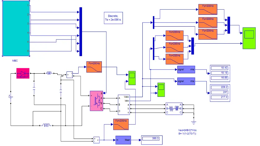
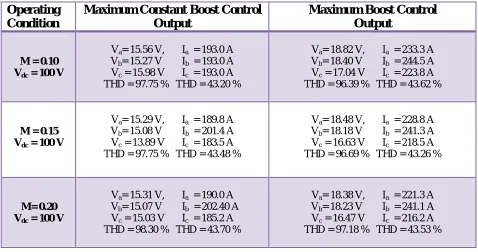
MATLAB simulations were performed to verify and compare different control methods. The SIMULINK model used is shown in Figure 5.1. The parameters used are: L1=L2= 1 mH, C1=C2=1000 μF, V=100 V (DC), Load: R/phase = 10 ohm, L/phase = 5 mH. The purpose of the system is to compare the performance of the different control techniques under different modulation indexes (M = 0.10, M = 0.15, and M = 0.20 respectively) with constant DC voltage input (100 V). A comparative analysis of voltage gain at different M is performed based on the mathematical calculation and simulation result for various control techniques. Results are shown in Figures 5.2 & 5.3 respectively.
Operating
Condition
Maximum Constant Boost Control
Output
Maximum Boost Control
Output
M = 0.10 Vdc = 100 V
Va= 15.56 V, Ia = 193.0 A
Vb= 15.27 V Ib = 193.0 A
Vc = 15.98 V Ic = 193.0 A
THD = 97.75 % THD = 43.20 %
Va= 18.82 V, Ia = 233.3 A
Vb= 18.40 V Ib = 244.5 A
Vc = 17.04 V Ic = 223.8 A
THD = 96.39 % THD = 43.62 %
M = 0.15 Vdc = 100 V
Va= 15.29 V, Ia = 189.8 A
Vb= 15.08 V Ib = 201.4 A
Vc = 13.89 V Ic = 183.5 A
THD = 97.75 % THD = 43.48 %
Va= 18.48 V, Ia = 228.8 A
Vb= 18.18 V Ib = 241.3 A
Vc = 16.63 V Ic = 218.5 A
THD = 96.69 % THD = 43.26 %
M= 0.20 Vdc = 100 V
Va= 15.31 V, Ia = 190.0 A
Vb= 15.07 V Ib = 202.40 A
Vc = 15.03 V Ic = 185.2 A
THD = 98.30 % THD = 43.70 %
Va= 18.38 V, Ia = 221.3 A
Vb= 18.23 V Ib = 241.1 A
Vc = 16.47 V Ic = 216.2 A
THD = 97.18 % THD = 43.53 %
Table I: Variations of fundamental output voltage, current and their THD level
Figure 5.2: Maximum Constant Boost Control.
VI. CONCLUSION
The three phase Z-source inverter has been simulated with modulation strategies namely maximum boost and maximum constant boost control. A comparison has been drawn between these control strategies and the performance parameters of the inverter have been investigated. This paper compares the performance of the different control techniques under different modulation indexes with constant DC voltage input. The better performances of the control methods of ZSI to achieve the maximum output within the prescribed limit of harmonics and THD percentages are obtained. The method can be achieved by the minimum passive components requirement and maintain low voltage stress at the same time.
REFERENCES
[1]. Amol R. Sutar, Satyawan R. Jagtap, Jakirhusen Tamboli, “Performance Analysis of Z-source Inverter Fed Induction Motor Drive in International Journal of Scientific & Engineering Research, Volume 3, Issue 5, May-2012 ISSN 2229-5518
[2]. Andreas Liske, Gerhard Clos and Michael Braun; “Analysis and Modeling of the Quasi-Z-Source-Inverter”
[3]. Cursino Brandao Jacobina, Antonio Marcus Nogueira Lima, “Current Control for Induction Motor Drives Using Random PWM” in IEEE Transactions On Industrial Electronics, VOL. 45, NO. 5, pp.704-712, 1998
[4]. F. Z. Peng: “Z-source inverter”, IEEE Transactions on Industry Applications, Vol. 39, No. 2, March/April 2003, pp.
[5]. Fang Zheng Peng, Miaosen Shen, Zhaoming Qian, “Maximum Boost Control of the Z-Source Inverter” IEEE Transactions on Power Electronics, vol. 20, no. 4, July 2005.
[6]. M. Baba, C. Lascu, I. Boldea; “Z converter control of a V/f induction motor drive” 13th International conference on Optimization of Electrical and Electronics Equipment 2012.
[7]. Miaosen Shen , Jin Wang ,Joseph A , Peng F. Z. , Tolbert, L.M. , Adams, D.J. ; “Maximum Constant Boost Miaosen Shen, Jin Wang, Alan Joseph, Fang Zheng
[8]. Miaosen Shen, Jin Wang, Alan Joseph, Fang Zheng Peng, Leon M. Tolbert, Donald J. Adams; “Constant Boost Control of the Z-Source Inverter to Minimize Current Ripple and Voltage Stress”, IEEE transactions on Industry Applications, vol. 42, no. 3, May/June 2006. [9]. Omar Ellabban, Joeri Van Mierlo and Philippe Lataire, “Comparison between Different PWM Control Methods for Different ZSource
Inverter Topologies” IEEE Transactions on industry application, May/June 2010
[10]. Omar Ellabban, Joeri Van Mierlo, and Philippe Lataire; Experimental Study of the Shoot-Through Boost Control Methods for the Z-Source Inverter.
[11]. Papavasiliou, S.A. Papathanassiou, “Current Control of a Voltage Source Inverter connected to the Grid via LCL Filter” in IEEE Trans. On Industry Applications, Vol. 37, No. 2,pp. 229-235, 2010
[12]. Poh Chiang Loh, Mahinda Vilathgamuwa, “Pulse-Width Modulation of Z-Source Inverters” in IEEE Transactions On Power Electronics, VOL. 20, NO.6, pp.1346-1355, 2005
[13]. S. Rajakaruna, Member, IEEE and Y. R. L. Jayawickrama, “Designing Impedance Network of Z-Source Inverters” IEEE Transactions on industry application.
[14]. Sivaraman.P, A. Nirmalkumar, “ Modelling and Simulation of Photovoltaic Array fed T-Source Inverter” in International Conference on Sustainable Energy and Intelligent System ,2011
[15]. Yuan Li, Joel Anderson, Fang Z. Peng, and Dichen Liu; “Quasi-Z-Source Inverter for Photovoltaic Power Generation Systems” Twenty – Sixth Annual IEEE on Applied Power Electronics Conference and Exposition 2011.
.
BIOGRAPHY
Sandeep Kumar Belongs to Allahabad Uttar Pradesh Received his Bachelor of Technology degree from Allahabad Agriculture Deemed University, Allahabad in 2013. He is pursuing his M.Tech in Electrical Engg. (Power Electronics) from SHIATS, Allahabad, UP-India. His field of interest includes power electronics, power converters and power quality.
Er. Vinay kumar tripathi belongs to district Allahabad of uttar pradesh. He received his bachelor of technology degree from UCER, allahabad in 2003. He obtained his M. Tech. in electrical eng. (control & instrumentation) from MNNIT, allahabad, Uttar pradesh in 2006 and pusuing Phd. from sam higginbottom institute of agriculture technology and sciences university (SHIATS), allahabad, up, india. He is having 10 years’ experience in teaching and presently working as asst. prof. in electrical engineering department, SSET, SHIATS, allahabad. His field of interest includes control and instrumentation, multiphase system, power quality and electric drive.