Zynq-7000 All
Programmable SoC:
Embedded Design
Tutorial
A Hands-On Guide to Effective
Embedded System Design
Revision History
The following table shows the revision history for this document.
Date Version Revision
06/13/2016 2016.2 Verified for 2016.2 versions of Vivado® Design Suite, Xilinx® SDK, and PetaLinux Tools.
05/09/2016 2016.1 Updated complete tutorial and reference design to tool chain version 2016.1 for Vivado, SDK, and PetaLinux Tools.
Added Chapter 9, Linux OS Aware Debugging Using SDK, which describes the new
Table of Contents
Revision History . . . 2
Chapter 1: Introduction
About This Guide . . . 5How Zynq Devices Simplify Embedded Processor Design . . . 7
How the Vivado Tools Expedite the Design Process . . . 9
What You Need to Set Up Before Starting . . . 10
Chapter 2: Using the Zynq SoC Processing System
Embedded System Configuration . . . 13Example Project: Creating a New Embedded Project with Zynq SoC . . . 14
Example Project: Running the “Hello World” Application . . . 26
Additional Information . . . 30
Chapter 3: Using the GP Port in Zynq Devices
Adding IP in PL to the Zynq SoC Processing System . . . 31Standalone Application Software for the Design. . . 41
Chapter 4: Debugging with SDK
Xilinx System Debugger . . . 44Debugging Software Using SDK. . . 46
Chapter 5: Using the HP Slave Port with AXI CDMA IP
Integrating AXI CDMA with the Zynq SoC PS HP Slave Port . . . 49Requirements . . . 90
Creating Peripheral IP . . . 91
Integrating Peripheral IP with PS GP Master Port . . . 96
Linux-Based Device Driver Development . . . 99
Loading Module into Running Kernel and Application Execution . . . 101
Chapter 8: Software Profiling Using SDK
Profiling an Application in SDK with System Debugger. . . 105Additional Design Support Options . . . 107
Chapter 9: Linux OS Aware Debugging Using SDK
Setting up Linux OS Aware Debugging . . . 109Debugging Linux Processes and Threads Using OS Aware Debug . . . 112
Appendix A: Additional Resources and Legal Notices
Xilinx Resources . . . 121Solution Centers. . . 121
Xilinx Documentation Navigator. . . 121
Design Files for This Tutorial . . . 122
Xilinx Resources . . . 122
Training Resources. . . 123
Chapter 1
Introduction
About This Guide
This document provides an introduction to using the Xilinx® Vivado® Design Suite flow for using the Zynq®-7000 All Programmable SoC device. The examples are targeted for the Xilinx ZC702 Rev 1.1 evaluation board and the tool version used is Vivado and the Xilinx Software Development Kit (SDK) 2016.2.
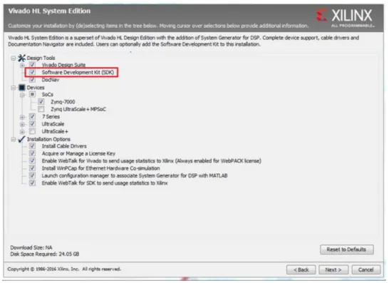
Note: To install SDK as part of the Vivado Design Suite, you must choose to include SDK in the
installer. See Xilinx Software Development Kit, page 9.
The examples in this document were created using the Xilinx tools running on Windows 7, 64-bit operating system. Other versions the tools running on other Window installs might provide varied results. These examples focus on introducing you to the following aspects of embedded design:
Note: The sequence mentioned in the tutorial steps for booting Linux on the hardware is specific
to the PetaLinux tools released for 2016.2, which must be installed on the Linux host machine for exercising the Linux portions of this document.
• Chapter 2, Using the Zynq SoC Processing System describes creation of a system with the Zynq SoC Processing System (PS) and running a simple "Hello World" application. This chapter is an introduction into the hardware and software tools using a simple design as the example.
• Chapter 3, Using the GP Port in Zynq Devices describes how to create a system using the Zynq SoC PS and the Programmable Logic (PL, or "fabric") and how to use a simple application to exercise both the PS and PL.
• Chapter 4, Debugging with SDK provides an introduction into debugging software using the debug features of the Xilinx Software Development Kit (SDK). This chapter
• Chapter 6, Linux Booting and Debug in SDK describes the steps to boot the Linux OS on the Zynq SoC board with PetaLinux Tools. This chapter provides information about instantiating the AXI CDMA IP in Fabric and integration with the High Performance (HP) 64 bit slave port.
• Chapter 7, Creating Custom IP and Device Driver for Linux guides you through creating Intellectual Property (IP) using the Create and Package New IP wizard. It describes Linux-based device driver development and kernel compilation. You will also design a system using your created IP for the Zynq device.
• Chapter 8, Software Profiling Using SDK describes the profiling feature for the Standalone BSP and the Application related to AXI CDMA, which is created in
Chapter 6. This highlights how to look at software and see if there are any bottlenecks. • Chapter 9, Linux OS Aware Debugging Using SDK describes the Linux OS aware
debugging feature and exercises it for Linux kernel and a basic Linux example. This is different from the Linux process debug already available in SDK. You can debug the Linux OS running on the Zynq ARM 9 processor cores and multiple application processes/threads running on the Linux OS simultaneously.
• Appendix A, Additional Resources and Legal Notices provides links to additional resources related to this guide.
Example Project
The best way to learn a tool is to use it. So, this guide provides opportunities for you to work with the tools under discussion. Specifications for sample projects are given in the example sections, along with an explanation of what is happening behind the scenes. Each chapter and examples are meant to showcase different aspects of embedded design. The example takes you through the entire flow to complete the learning and then moves on to another topic.
Additional Documentation
Chapter 1: Introduction
How Zynq Devices Simplify Embedded Processor
Design
Embedded systems are complex. Hardware and software portions of an embedded design are projects in themselves. Merging the two design components so that they function as one system creates additional challenges. Add an FPGA design project to the mix, and your design has the potential to become very complicated.
The Zynq SoC solution reduces this complexity by offering an ARM Cortex-A9 dual core, along with programmable logic, all within a single SoC.
To simplify the design process, Xilinx offers the Vivado Design Suite and the Xilinx Software Development Kit (SDK). This set of tools provides you with everything you need to simplify embedded system design for a device that merges an SoC with an FPGA. This combination of tools offers hardware and software application design, debugging capability, code execution, and transfer of the design onto actual boards for verification and validation.
Note: To install SDK as part of the Vivado Design Suite, you must elect to include SDK in the installer.
See Xilinx Software Development Kit, page 9.
The Vivado Design Suite, System Edition
Xilinx offers a broad range of development system tools, collectively called the Vivado Design Suite. Various Vivado Design Suite Editions can be used for embedded system development. In this guide we will utilize the System Edition. The Vivado Design Suite Editions are shown in the following figure.
Other Vivado Components
Other Vivado components include:
• Embedded/Soft IP for the Xilinx embedded processors • Documentation
• Sample projects
X-Ref Target - Figure 1-1
Chapter 1: Introduction
Xilinx Software Development Kit
The Software Development Kit (SDK) is an integrated development environment,
complementary to Vivado, that is used for C/C++ embedded software application creation and verification. SDK is built on the Eclipse open-source framework and might appear familiar to you or members of your design team.
When you install the Vivado Design Suite, SDK is available as an optional software tool that you must choose to include in your installation. For details, refer to Installation
Requirements, page 10.
For more information about the Eclipse development environment, refer to
http://www.eclipse.org.
Other SDK components include:
• Drivers and libraries for embedded software development
• GNU compiler and debugger for C/C++ software development targeting the ARM Cortex-A9 MP processors in the Zynq SoC Processing System
PetaLinux Tools
The PetaLinux tools set is an Embedded Linux System Development Kit. It offers a full Linux distribution which includes the Linux OS as well as a complete configuration, build, and deploy environment for Xilinx silicon.
For more information, refer to the Xilinx PetaLinux web page [Ref 17].
The PetaLinux Tools design hub provides information and links to documentation specific to PetaLinux Tools. For more information, refer to Related Design Hubs, page 121.
How the Vivado Tools Expedite the Design Process
You can use the Vivado Design Suite tools to add design sources to your hardware. These include the IP integrator, which simplifies the process of adding IP to your existing project
The Zynq SoC Processing System (PS) can be booted and made to run without
programming the FPGA (programmable logic or PL). However, in order to use any soft IP in the fabric, or to bond out PS peripherals using EMIO, programming of the PL is required. You can program the PL in SDK.
For more information on the embedded design process, refer to the Vivado Design Suite Tutorial: Embedded Processor Hardware Design (UG940) [Ref 6].
What You Need to Set Up Before Starting
Before discussing the tools in depth, you should make sure they are installed properly and your environments match those required for the "Example Project" sections of this guide.
Hardware Requirements for this Guide
This tutorial targets the Zynq ZC702 Rev 1.1 evaluation board, and can also be used for Rev 1.0 boards. To use this guide, you need the following hardware items, which are included with the evaluation board:
• The ZC702 evaluation board • AC power adapter (12 VDC)
• USB Type-A to USB Mini-B cable (for UART communications)
• USB Type-A to USB Micro cable for programming and debugging via USB-Micro JTAG connection
• SD-MMC flash card for Linux booting
• Ethernet cable to connect target board with host machine
Installation Requirements
Vivado Design Suite and SDK
Make sure that you have installed the 2016.2 software. Visit http://www.xilinx.com/support/ download.html to confirm that you have the latest software version.
Ensure that you have both the Vivado Design Suite and SDK Tools installed. When you install the Vivado Design Suite, SDK is available as an optional software tool that you must elect to include in your installation by selecting the Software Development Kit check box, as shown in the following figure. To install SDK by itself, you can deselect the other software products and run the installer with only Software Development Kit selected.
Chapter 1: Introduction
For more information on installing the Vivado Design Suite and SDK, refer to the Vivado Design Suite User Guide: Release Notes, Installation, and Licensing (UG973) [Ref 7].
IMPORTANT: Installation does not create an SDK desktop shortcut by default. You can launch the SDK binary from C:\Xilinx\SDK\2016.2\bin\xsdk.bat.
PetaLinux Tools
Install the PetaLinux Tools to run through the Linux portion of this tutorial. PetaLinux tools run under the Linux host system running one of the following:
• RHEL 6 (32-bit or 64-bit)
• SUSE Enterprise 11 (32-bit or 64-bit) • CentOS (64-bit)
X-Ref Target - Figure 1-2
When you install PetaLinux Tools on your system of choice, you must do the following: • Download PetaLinux 2016.2 SDK software from the Xilinx Website.
• Install the PetaLinux 2016.2 release package.
• Add common system packages and libraries to the workstation or virtual machine.
Prerequisites
• 2 GB RAM (recommended minimum for Xilinx tools) • Pentium 4 2GHz CPU clock or equivalent
• 5 GB free HDD space
Extract the PetaLinux Package
By default, the installer installs the package as a subdirectory within the current directory. Alternatively, you can specify an installation path. Run the downloaded PetaLinux installer.
Note: Ensure that the PetaLinux installation path is kept short. The PetaLinux build will fail if the path
exceeds 255 characters.
bash> ./petalinux-v2016.2-final-installer.run
PetaLinux is installed in the petalinux-v2016.2-final directory, directly underneath
the working directory of this command. If the installer is placed in the home directory
/home/user, PetaLinux is installed in /home/user/petalinux-v2016.2-final.
Refer to Chapter 6, Linux Booting and Debug in SDK for additional information about the PetaLinux environment setup, project creation, and project usage examples. A detailed guide on PetaLinux Installation and usage can be found in the PetaLinux Tools
Documentation Reference Guide (UG1144) [Ref 11].
Software Licensing
Xilinx software uses FLEXnet licensing. When the software is first run, it performs a license verification process. If the license verification does not find a valid license, the license wizard guides you through the process of obtaining a license and ensuring that the license can be used with the tools installed. If you do not need the full version of the software, you can use an evaluation license.For installation instructions and information, see the Vivado Design Suite User Guide: Release Notes, Installation, and Licensing (UG973) [Ref 7].
Tutorial Design Files
See Design Files for This Tutorial, page 122 for information about downloading the design files for this tutorial.
Chapter 2
Using the Zynq SoC Processing System
Now that you have been introduced to the Xilinx® Vivado® Design Suite, you will begin looking at how to use it to develop an embedded system using the Zynq®-7000 AP SoC Processing System (PS).
The Zynq SoC consists of ARM Cortex™-A9 cores, many hard intellectual property components (IPs), and programmable logic (PL). This offering can be used in two ways: • The Zynq SoC PS can be used in a standalone mode, without attaching any additional
fabric IP.
• IP cores can be instantiated in fabric and attached to the Zynq PS as a PS+PL combination.
Embedded System Configuration
Creation of a Zynq device system design involves configuring the PS to select the
appropriate boot devices and peripherals. To start with, as long as the PS peripherals and available MIO connections meet the design requirements, no bitstream is required. This chapter guides you through creating a simple PS-based design that does not require a bitstream.
Example Project: Creating a New Embedded Project
with Zynq SoC
For this example, you will launch the Vivado Design Suite and create a project with an embedded processor system as the top level.
Starting Your Design
1. Start the Vivado Design Suite.
2. In the Vivado Quick Start page, click Create New Project to open the New Project wizard.
3. Use the information in the table below to make selections in each of the wizard screens.
4. Click Finish. The New Project wizard closes and the project you just created opens in the Vivado design tool.
Wizard Screen System Property Setting or Command to Use
Project Name Project name edt_tutorial
Project Location C:/designs
Create Project Subdirectory Leave this checked
Project Type Specify the type of sources for your
design. You can start with RTL or a synthesized EDIF.
RTL Project
Do not specify sources at this
time check box Leave this unchecked
Add Sources Do not make any changes to this screen.
Add Existing IP Do not make any changes to this screen.
Add Constraints Do not make any changes to this screen.
Default Part Select Boards
Board ZYNQ-7 ZC702 Evaluation Board
New Project Summary Project Summary Review the project summary before
Chapter 2: Using the Zynq SoC Processing System
Creating an Embedded Processor Project
You will now use the Add Sources wizard to create an embedded processor project. 1. In the Flow Navigator, under IP Integrator, click Create Block Design.
The Create Block Design wizard opens.
2. Use the following information to make selections in the Create Block Design wizard.
3. Click OK.
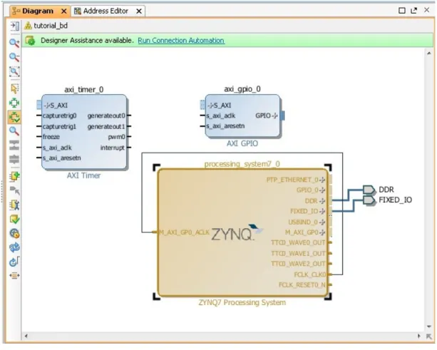
The Diagram window view opens with a message that states that this design is empty. To get started, you will next add some IP from the catalog.
4. Click the Add IP button .
5. In the search box, type zynq to find the Zynq device IP options.
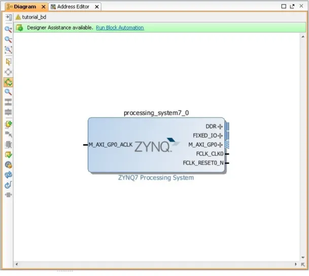
6. Double-click the ZYNQ Processing System IP to add it to the Block Design.
The Zynq MPSoC processing system IP block appears in the Diagram view, as shown in the following figure.
X-Ref Target - Figure 2-1
Figure 2-1: Create Block Design Button
Wizard Screen System Property Setting or Command to Use
Create Block Design Design Name tutorial_bd
Directory <Local to Project>
X-Ref Target - Figure 2-2
Chapter 2: Using the Zynq SoC Processing System
Managing the Zynq7 Processing System in Vivado
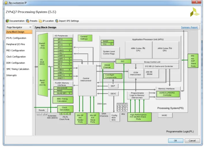
Now that you have added the processor system for the Zynq SoC to the design, you can begin managing the available options.
1. Double-click the ZYNQ7 Processing System block in the Block Diagram window. The Re-customize IP dialog box opens, as shown in the following figure. Notice that by default, the processor system does not have any peripherals connected.
X-Ref Target - Figure 2-3
Note the check marks that appear next to each peripheral name in the Zynq device block diagram that signify the I/O Peripherals that are active.
3. In the block diagram, click one of the green I/O Peripherals. The MIO Configuration window opens for the selected peripheral.
X-Ref Target - Figure 2-4
Figure 2-4: I/O Peripherals with Active Peripherals Identified
Chapter 2: Using the Zynq SoC Processing System
4. Click OK to close the Re-customize IP wizard. Vivado implements the changes that you made to apply the ZC702 board presets.
In the Block Diagram window, notice the message stating that Designer assistance is available, as shown in the following figure.
5. Click the Run Block Automation link.
The Run Block Automation dialog box opens.
Note that Cross Trigger In and Cross Trigger Out are disabled. For a detailed tutorial with information about cross trigger set-up, refer to the Vivado Design Suite Tutorial: Embedded Processor Hardware Design (UG940) [Ref 6].
6. Click OK to accept the default processor system options and make default pin connections.
Validating the Design and Connecting Ports
Now, validate the design.
1. Right-click in the white space of the Block Diagram view and select Validate Design. Alternatively, you can press the F6 key.
2. A critical error message appears, indicating that the M_AXI_GP0_ACLK must be
connected.
X-Ref Target - Figure 2-6
Figure 2-6: Run Block Automation Link
3. Click OK to clear the message.
4. In the Block Diagram view of the ZYNQ7 Processing System, locate the
M_AXI_GP0_ACLK port. Hover your mouse over the connector port until the pencil icon
appears.
5. Click the M_AXI_GP0_ACLK port and drag to the FCLK_CLK0 input port to make a connection between the two ports.
6. Validate the design again to ensure there are no other errors. To do this, right-click in the white space of the Block Diagram view and select Validate Design.
A message dialog box opens and states "Validation successful. There are no errors or critical warnings in this design."
7. Click OK to close the message.
8. In the Block Design view, click the Sources tab. 9. Click Hierarchy.
10. Under Design Sources, right-click tutorial_bd and select Create HDL Wrapper.
The Create HDL Wrapper dialog box opens. You will use this dialog box to create a HDL wrapper file for the processor subsystem.
TIP: The HDL wrapper is a top-level entity required by the design tools.
11. Select Let Vivado manage wrapper and auto-update and click OK. 12. In the Block Diagram, Sources window, under Design Sources, expand
tutorial_bd_wrapper.
X-Ref Target - Figure 2-8
Chapter 2: Using the Zynq SoC Processing System
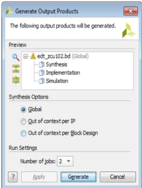
13. Right-click the top-level block diagram, titled tutorial_bd_i - tutorial_bd (tutorial_bd.bd) and select Generate Output Products.
Note: The Generate Output Products dialog box opens, as shown in the following
figure.If you are running the Vivado Design Suite on a Linux host machine, you might see
additional options under Run Settings. In this case, continue with the default settings.
14. Click Generate.
This step builds all required output products for the selected source. For example, constraints do not need to be manually created for the IP processor system. The Vivado tools automatically generate the XDC file for the processor sub-system when Generate Output Products is selected.
15. When the Generate Output Products process completes, click OK.
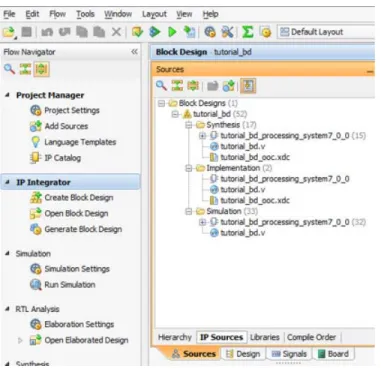
16. In the Block Diagram Sources window, click the IP Sources tab.Here you can see the output products that you just generated, as shown in the following figure.
X-Ref Target - Figure 2-9
Synthesizing the Design, Running Implementation, and
Generating the Bitstream
1. You can now synthesize the design. In the Flow Navigator pane, under Synthesis, click
Run Synthesis.
2. If Vivado prompts you to save your project before launching synthesis, click Save. While synthesis is running, a status bar displays in the upper right-hand window. This status bar spools for various reasons throughout the design process. The status bar signifies that a process is working in the background.
When synthesis completes, the Synthesis Completed dialog box opens.
X-Ref Target - Figure 2-10
Figure 2-10: Outputs Generated Under IP Sources
X-Ref Target - Figure 2-11
Figure 2-11: Run Synthesis Button
X-Ref Target - Figure 2-12
Chapter 2: Using the Zynq SoC Processing System
3. Select Run Implementation and click OK.
Again, notice that the status bar describes the process running in the background. When implementation completes, the Implementation Completed dialog box opens.
4. Select Generate Bitstream and click OK.
When Bitstream Generation completes, the Bitstream Generation Completed dialog box opens.
5. Click Cancel to close the window.
6. After the Bitstream generation completes, export the hardware and launch the Software Development Kit (SDK) as described in the next section.
Exporting to SDK
In this example, you will launch SDK from Vivado.
1. From the Vivado toolbar, select File > Export > Export Hardware.
The Export Hardware dialog box opens. Make sure that the Include bitstream check box is checked (only when design has PL design and bitstream generated), and that the
Export to field is set to the default option of <Local to Project>.
2. Click OK.
TIP: The hardware is exported in a ZIP file (<project wrapper>.hdf). When SDK launches, the file unzips automatically, and you can find all the files in the SDK project hardware platform folder.
X-Ref Target - Figure 2-13
4. Accept the default selections for Exported location and Workspace.
5. Click OK.
SDK opens. Notice that when SDK launches, the hardware description file is loaded automatically. The system.hdf tab shows the address map for the entire Processing
System, as shown in the following figure.
6. Close SDK.
X-Ref Target - Figure 2-14
Figure 2-14: Launch SDK Dialog Box
X-Ref Target - Figure 2-15
Chapter 2: Using the Zynq SoC Processing System
What Just Happened?
Vivado exported the hardware specifications to the selected workspace where software development will take place. If <Local to Project> was selected, then Vivado created a new workspace in the Vivado project folder. The name of the workspace is
<project_name>.sdk. In this example, the workspace created is C:/designs/edt_tutorial/edt_tutorial.sdk.
The Vivado design tool exported the Hardware Platform Specification for your design (system.hdf in this example) to SDK. In addition to system.hdf, the following additional
files are exported to SDK: • design_1_bd.tcl • ps7_init.c • ps7_init.h • ps7_init.html • ps7_init.tcl • ps7_init_gpl.c • ps7_init_gpl.h • system.hdf
The system.hdf file opens by default when SDK launches. The address map of your
system read from this file is shown by default in the SDK window.
The ps7_init.c, ps7_init.h, ps7_init_gpl.c, and ps7_init_gpl.h files contain
the initialization code for the Zynq SoC Processing System and initialization settings for DDR, clocks, phase-locked loops (PLLs), and MIOs. SDK uses these settings when initializing the processing system so that applications can be run on top of the processing system. Some settings in the processing system are fixed for the ZC702 evaluation board.
What's Next?
Now you can start developing the software for your project using SDK. The next sections help you create a software application for your hardware platform.
Example Project: Running the “Hello World”
Application
In this example, you will learn how to manage the board settings, make cable connections, connect to the board through your PC, and run a simple hello world software application in JTAG mode using System Debugger in Xilinx SDK.
1. Connect the power cable to the board.
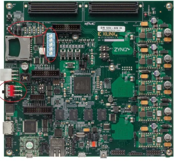
2. Connect a USB Micro cable between the Windows Host machine and the Target board with the following SW10 switch settings:
Bit-1 is 0 Bit-2 is 1
Note: 0 = switch is open. 1 = switch is closed.
3. Connect a USB cable to connector J17 on the target board with the Windows Host machine. This is used for USB to serial transfer.
4. Power on the ZC702 board using the switch indicated in the figure below.
IMPORTANT: Ensure that jumper s J27 and J28 are placed on the side farther from the SD card slot and change the SW16 switch setting as shown in the following figure.
Chapter 2: Using the Zynq SoC Processing System
5. Open SDK and set the workspace path to your project file, which in this example is
C:/designs/edt_tutorial/edt_tutorial.sdk.
Alternately, you can open SDK with a default workspace and later switch it to the correct workspace by selecting File > Switch Workspace and then selecting the workspace. 6. Open a serial communication utility for the COM port assigned on your system. SDK
provides a serial terminal utility, which will be used throughout the tutorial; select
Window > Show View > Terminal to open it.
X-Ref Target - Figure 2-16
Figure 2-16: ZC702 Board Power Switch
The following figure shows the standard configuration for the Zynq SoC Processing System.
9. Select File > New > Application Project. The New Project wizard opens.
10. Use the information in the following table to make your selections in the wizard screens.
SDK creates the hello_world application project and hello world_bsp board
support package (BSP) project under the Project Explorer. It automatically compiles both
X-Ref Target - Figure 2-18
Figure 2-18: Terminal Settings Dialog Box
Wizard Screen System Properties Setting or Command to Use
Application Project Project Name hello_world
Use Default Location Select this option
Hardware Platform tutorial_bd_wrapper_hw_platform_0
Processor PS7_cortexa9_0
OS Platform standalone
Language C
Board Support Package Select Create New and provide the name
of hello_world_bsp.
Chapter 2: Using the Zynq SoC Processing System IMPORTANT: If you would like to regenerate the BSP, right-click the BSP project under the Project Explorer and select Re-generate BSP Sources.
If you would like to change the target BSP after project creation: 1. Create a New Board Support Package for your target.
2. In the Project Explorer, right click your application project and select Change Referenced BSP, and point the new BSP you want to set.
11. Right-click hello_world and select Run as > Run Configurations.
12. Right-click Xilinx C/C++ application (System Debugger) and click New.
SDK creates the new run configuration, named hello_world Debug.
The configurations associated with the application are pre-populated in the Main tab of the launch configurations.
13. Click the Target Setup tab and review the settings.
Notice that there is a configuration path to the initialization TCL file. The path of
ps7_init.tcl is mentioned here. This file was exported when you exported your
design to SDK; it contains the initialization information for the processing system. 14. Click Run.
"Hello World" appears on the serial communication utility in Terminal 1, as shown in
the following figure.
Note: There was no bitstream download required for the above software application to be executed
on the Zynq SoC evaluation board. The ARM Cortex A9 dual core is already present on the board. Basic initialization of this system to run a simple application is done by the Device initialization TCL script.
What Just Happened?
X-Ref Target - Figure 2-19Additional Information
Board Support Package
The board support package (BSP) is the support code for a given hardware platform or board that helps in basic initialization at power up and helps software applications to be run on top of it. It can be specific to some operating systems with bootloader and device drivers.
Standalone OS
Standalone is a simple, low-level software layer. It provides access to basic processor features such as caches, interrupts, and exceptions, as well as the basic processor features of a hosted environment. These basic features include standard input/output, profiling, abort, and exit. It is a single threaded semi-hosted environment.
T
IMPORTANT: The application you ran in this chapter was created on top of the Standalone OS. The BSP that your software application targets is selected during the New Application Project creation process. If you would like to change the target BSP after project creation, you can manage the target BSP by right-clicking the software application and selecting Change Referenced BSP.
Chapter 3
Using the GP Port in Zynq Devices
One of the unique features of using the Xilinx® Zynq®-7000 AP SoC as an embedded
design platform is in using the Zynq SoC Processing System (PS) for its ARM Cortex-A9 dual core processing system as well as the Programmable Logic (PL) available on it.
In this chapter, you will create a design with:
• AXI GPIO and AXI Timer in fabric (PL) with interrupt from fabric to PS section • Zynq SoC PS GPIO pin connected to the fabric (PL) side pin via the EMIO interface The flow of this chapter is similar to that in Chapter 2 and uses the Zynq device as a base hardware design. It is assumed that you understand the concepts discussed in Chapter 2
regarding adding the Zynq device into a Vivado® IP integrator block diagram design. If you
skipped that chapter, you might want to look at it because we will continually refer to the material in Chapter 2 throughout this chapter.
Adding IP in PL to the Zynq SoC Processing System
There is no restriction on the complexity of an intellectual property (IP) that can be added in fabric to be tightly coupled with the Zynq SoC PS. This section covers a simple example with the AXI GPIO, AXI Timer with interrupt, and the PS section GPIO pin connected to PL side pin via the EMIO interface.
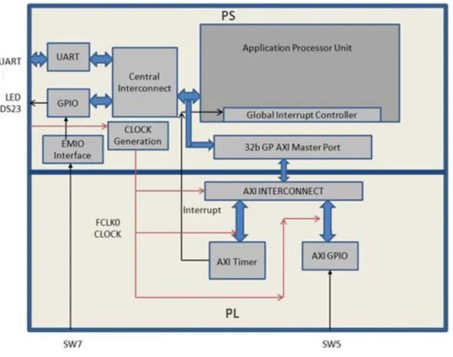
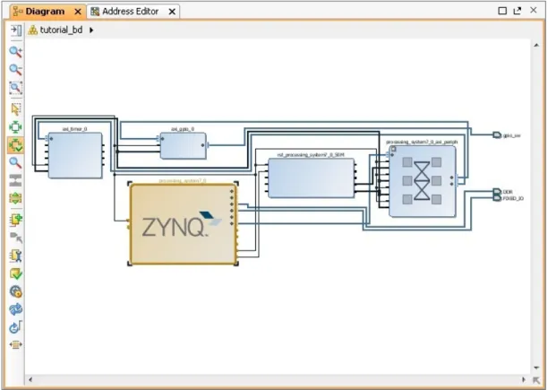
In this section, you will create a design to check the functionality of the AXI GPIO, AXI Timer with interrupt instantiated in fabric, and PS section GPIO with EMIO interface. The block diagram for the system is as shown in the following figure.
You can use the system created in Chapter 2 and continue after Example Project: Creating a New Embedded Project with Zynq SoC, page 14.
In the examples in this chapter, we will expand on the design in Chapter 2. You will make the following design changes:
• The fabric-side AXI GPIO is assigned a 1-bit channel width and is connected to the SW5 push-button switch on the ZC702 board.
• The PS GPIO ports are modified to include a 1-bit interface that routes a fabric pin (via the EMIO interface) to the SW7 push-button switch on the board.
• In the PS section, another 1-bit GPIO is connected to the DS23 LED on the board, which is on the MIO port.
• The AXI timer interrupt is connected from fabric to the PS section interrupt controller. The timer starts when you press any of the selected push buttons on the board. After the timer expires, the timer interrupt is triggered.
X-Ref Target - Figure 3-1
Chapter 3: Using the GP Port in Zynq Devices
• Along with making the above hardware changes, you will write the application software code. The code will function as follows:
° A message appears in the serial terminal and asks you to select the push button
switch to use on the board (either SW7 or SW5).
° When the appropriate button is pressed, the timer automatically starts, switches
OFF LED DS23, and waits for the timer interrupt to happen.
° After the Timer Interrupt, LED DS23 switches ON and execution starts again and
waits for you to again select the push button switch in the serial terminal.
Example Project: Validate Instantiated Fabric IP Functionality
In this example, you will add the AXI GPIO, AXI Timer, the interrupt instantiated in fabric, and the EMIO interface. You will then validate the fabric additions.
1. Open the Vivado® Design Suite.
2. Under the Recent Projects column, click the edt_tutorial design that you created in
Chapter 2.
3. Under IP Integrator, click Open Block Design.
4. In the Diagram window, right-click in the blank space and select Add IP.
5. In the search box, type AXI GPIO and double-click the AXI GPIO IP to add it to the
Block Design.
The AXI GPIO IP block appears in the Diagram view.
6. In the Diagram window, right-click in the blank space and select Add IP.
7. In the search box, type AXI Timer and double-click the AXI Timer IP to add it to the
Block Design. The AXI Timer IP block appears in the Diagram view.
8. You must also edit the EMIO configuration of the ZYNQ7 SoC Processing system and enable interrupts. Right-click the ZYNQ7 Processing System IP block and select
Customize Block.
Note: You can also double-click the IP block to customize.
9. Click MIO Configuration.
10. Expand I/O Peripherals > GPIO and select the EMIO GPIO (Width) check box. 11. Change the EMIO GPIO (Width) to 1.
12. With the ZYNQ7 Processing System configuration options still open, navigate to
Interrupts > Fabric Interrupts > PL-PS Interrupt Ports.
13. Check the Fabric Interrupts box and also check IRQ_F2P[15:0] to enable PL-PS interrupts in the IP Core.
14. Click OK to accept the changes to the ZYNQ7 Processing System IP. The Diagram looks like the following figure.
X-Ref Target - Figure 3-2
Chapter 3: Using the GP Port in Zynq Devices
15. Click the Run Connection Automation link at the top of the page to automate the connection process for the newly added IP blocks.
16. In the Run Connection Automation wizard, select the check box next to All Automation, as shown in the following figure.
X-Ref Target - Figure 3-3
Figure 3-3: ZYNQ7 Processing System IP
Upon completion, the updated diagram looks like the following figure.
18. Right-click the AXI GPIO IP block and select Customize Block.
Note: You can also double-click the IP block to make customizations.
19. Under the Board tab, make sure that both GPIO and GPIO2 are set to Custom. 20. Select the IP Configuration tab. In the GPIO section, change the GPIO Width to 1
because you only need one GPIO port. Also ensure that All Inputs and All Outputs are both unchecked.
21. Click OK to accept the changes.
22. Notice that the Interrupt port is not automatically connected to the AXI Timer IP Core. In the Block Diagram view, locate the IRQ_F2P[0:0] port on the ZYNQ7 Processing
System.
23. Scroll your mouse over the connecter port until the pencil icon appears, then click the
IRQ_F2P[0:0] port and drag to the interrupt output port on the AXI Timer IP core to make a connection between the two ports.
X-Ref Target - Figure 3-5
Chapter 3: Using the GP Port in Zynq Devices
24. Notice that the ZYNQ7 Processing System GPIO_0 port is not connected. Right-click the
GPIO_0 output port on the ZYNQ7 Processing System and select Make External. The pins are external but do not have the needed constraints for our board. In order to constrain your hardware pins to specific device locations, follow the steps below. These steps can be used for any manual pin placements.
25. Click Open Elaborated Design under RTL Analysis in the Flow Navigator view.
26. When the Elaborate Design message box opens, as shown in the following figure, click
OK.
TIP: The design might take a few minutes to elaborate. If you want to do something else in
Vivado while the design elaborates, you can click the Background button to have Vivado continue running the process in the background.
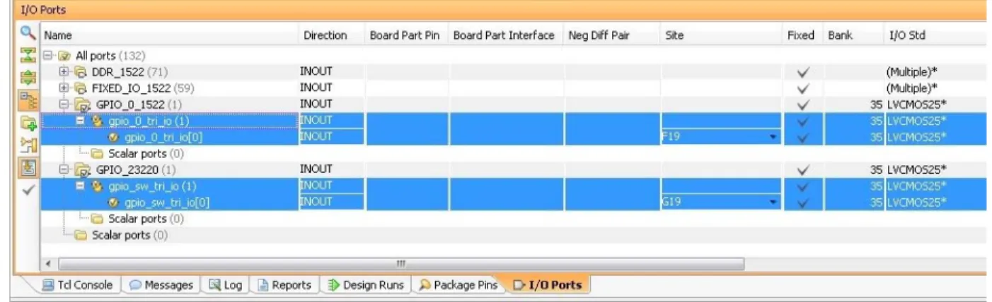
27. Select I/O Planning from the drop-down menu, as shown in the following figure, to display the I/O Ports tab.
X-Ref Target - Figure 3-6
Figure 3-6: Open Elaborated Design
X-Ref Target - Figure 3-7
28. Under the I/O Ports tab view at the bottom of the Vivado window (as seen in the following figure), expand the GPIO_0_1522 and GPIO_23220 ports to check the site (pin) map.
29. Find gpio_0_tri_io[0] and set the following properties, shown in Figure 3-10:
° Site = F19
° I/O Std = LVCMOS25
30. Find gpio_sw_tri_io[0] and set the following properties, shown in Figure 3-10:
° Site = G19
° I/O Std = LVCMOS25
X-Ref Target - Figure 3-8
Figure 3-8: I/O Planning Selection
X-Ref Target - Figure 3-9
Chapter 3: Using the GP Port in Zynq Devices
Note: For additional information about creating other design constraints, refer to the Vivado
Design Suite User Guide: Using Constraints (UG903) [Ref 4].
31. In the Flow Navigator, under Program and Debug, select Generate Bitstream.
The Save Project dialog box opens. Make sure the Elaborated Design - constrs_1 check box is selected and click Save.
If the Synthesis is Out-of-date dialog box opens, click Yes to re-run synthesis.
32. The Save Constraints popup window appears (shown in the following figure). Provide a file name and click OK.
X-Ref Target - Figure 3-10
Figure 3-10: I/O Port Properties
33. After Bitstream generation completes, export the hardware and launch the Xilinx Software Development Kit (SDK) as described in Exporting to SDK, page 23.
Working with SDK
1. SDK launches with the Hello World project you created with the Standalone PS in Chapter 2.
2. Select Project > Clean to clean and build the project again.
3. Open the helloworld.c file and modify the application software code as described in
Standalone Application Software for the Design, in Standalone Application Software for the Design, page 41.
4. Open the serial communication utility with baud rate set to 115200.
Note: This is the baud rate that the UART is programmed to on Zynq devices.
5. Connect to the board.
Because you have a bitstream for the PL Fabric, you must download the bitstream. 6. Select Xilinx Tools > Program FPGA. The Program FPGA dialog box, shown in
Figure 3-13, opens. It displays the bitstream exported from Vivado.
X-Ref Target - Figure 3-12
Chapter 3: Using the GP Port in Zynq Devices
7. Click Program to download the bitstream and program the PL Fabric.
8. Run the project similar to the steps in Example Project: Running the “Hello World” Application, page 26.
9. In the system, the AXI GPIO pin is connected to push button SW5 on the board, and the PS section GPIO pin is connected to push button SW7 on the board via an EMIO interface.
10. Follow the instructions printed on the serial terminal to run the application.
Standalone Application Software for the Design
The system you designed in this chapter requires application software for the execution on
X-Ref Target - Figure 3-13
Application Software Steps
Application Software is composed of the following steps: 1. Initialize the AXI GPIO module.
2. Set a direction control for the AXI GPIO pin as an input pin, which is connected with the
SW5 push button on the board. The location is fixed via LOC constraint in the user constraint file (XDC) during system creation.
3. Initialize the AXI TIMER module with device ID 0. 4. Associate a timer callback function with AXI timer ISR.
This function is called every time the timer interrupt happens. This callback switches on the LED DS23 on the board and sets the interrupt flag.
The main() function uses the interrupt flag to halt execution, waits for timer interrupt
to happen, and then restarts the execution.
5. Set the reset value of the timer, which is loaded to the timer during reset and timer starts.
6. Set timer options such as Interrupt mode and Auto Reload mode. 7. Initialize the PS section GPIO.
8. Set the PS section GPIO, channel 0, pin number 10 to the output pin, which is mapped to the MIO pin and physically connected to the LED DS23 on the board.
9. Set PS Section GPIO channel number 2, pin number 0, to an input pin, which is mapped to PL side pin via the EMIO interface and physically connected to the SW7 push button switch.
10. Initialize Snoop control unit Global Interrupt controller. Also, register Timer interrupt routine to interrupt ID '91', register the exceptional handler, and enable the interrupt. 11. Execute a sequence in the loop to select between AXI GPIO or PS GPIO use case via serial
terminal.
The software accepts your selection from the serial terminal and executes the procedure accordingly.
After the selection of the use case via the serial terminal, you must press a push button on the board as per the instruction on terminal. This action switches off the LED DS23, starts the timer, and tells the function to wait infinitely for the Timer interrupt to happen. After the Timer interrupt happens, LED DS23 switches ON and restarts execution.
For more details about API related to device drivers, refer to the Zynq-7000 All Programmable SoC Software Developers Guide (UG821) [Ref 3].
Chapter 3: Using the GP Port in Zynq Devices
Application Software Code
The Application software for the system is included in helloworld.c, which is available in
the ZIP file that accompanies this guide. See Design Files for This Tutorial, page 122.
Run the New Software Application in SDK
Next, you will run the new software application in SDK. 1. Select Xilinx Tools > Program FPGA.
The Program FPGA dialog box, shown in the following figure, opens. It displays the bitstream exported from Vivado.
X-Ref Target - Figure 3-14
Debugging with SDK
This chapter describes debug possibilities with the design flow you have already been working with. The first option is debugging with software using the Xilinx® Software Development Kit (SDK).
SDK debugger provides the following debug capabilities:
• Supports debugging of programs on MicroBlaze™ and ARM Cortex-A9 processor architectures (heterogeneous multi-processor hardware system debugging) • Supports debugging of programs on hardware boards
• Supports debugging on remote hardware systems • Provides a feature-rich IDE to debug programs
• Provides a Tool Command Language (Tcl) interface for running test scripts and automation
The SDK debugger enables you to see what is happening to a program while it executes. You can set breakpoints or watchpoints to stop the processor, step through program execution, view the program variables and stack, and view the contents of the memory in the system.
Xilinx SDK supports debugging through Xilinx System Debugger and GNU Debugger (GDB).
Note: The GDB flow is deprecated and will not be available for future devices.
Xilinx System Debugger
The Xilinx System Debugger uses the Xilinx hw_server as the underlying debug engine. SDK translates each user interface action into a sequence of Target Communication Framework (TCF) commands. It then processes the output from System Debugger to display the current state of the program being debugged. It communicates to the processor on the hardware using Xilinx hw_server.
Chapter 4: Debugging with SDK
The workflow is made up of the following components:
• Executable ELF File: To debug your application, you must use an Executable and Linkable Format (ELF) file compiled for debugging. The debug ELF file contains additional debug information for the debugger to make direct associations between the source code and the binaries generated from that original source. To manage the build configurations, right-click the software application and select Build
Configurations > Manage.
• Debug Configuration: To launch the debug session, you must create a debug configuration in SDK. This configuration captures options required to start a debug session, including the executable name, processor target to debug, and other
information. To create a debug configuration, right-click your software application and select Debug As > Debug Configurations.
• SDK Debug Perspective: Using the Debug perspective, you can manage the
debugging or running of a program in the Workbench. You can control the execution of
X-Ref Target - Figure 4-1
Figure 4-1: System Debugger Flow
6SHFLI\ KZBVHUYHU GHWDLOV &UHDWH'HEXJ &RQILJXUDWLRQ 6'.'HEXJ 3HUVSHFWLYH KZBVHUYHU 3URJUDPUXQQLQJ RQ+DUGZDUH RU,66 HOI Debug Executable ;
Debugging Software Using SDK
In this example, you will walk through debugging a hello world application.
If you modified the hello world application in the prior chapter, you will need to create a new hello world application prior to debugging. Follow the steps in Example Project: Running the “Hello World” Application, page 26 to create a new hello world application. After you create the Hello World Application, work through the below example to debug the software using SDK.
1. In the C/C++ Perspective, right-click the Hello_world Project and select Debug As >
Launch on Hardware (System Debugger).
If the Confirm Perspective Switch popup window appears, click Yes. The Debug Perspective opens.
X-Ref Target - Figure 4-2
Chapter 4: Debugging with SDK
Note: If the Debug Perspective window does not automatically open, select Window > Open >
Perspective > Other, then select Debug in the Open Perspective wizard.
Note: The addresses shown on this page might slightly differ from the addresses shown on your
system.
The processor is currently sitting at the beginning of main() with program execution
suspended at line 0x0010054c. You can confirm this information in the Disassembly
view, which shows the assembly-level program execution also suspended at
0x0010054c.
Note: If the Disassembly view is not visible, select Window > Show View > Disassembly.
2. The helloworld.c window also shows execution suspended at the first executable
line of C code. Select the Registers view to confirm that the program counter, pc register, contains 0x0010054c.
Note: If the Registers window is not visible, select Window > Show View > Registers.
X-Ref Target - Figure 4-3
4. Select Run > Step Into to step into the init_platform () routine.
Program execution suspends at location 0x001005c4. The call stack is now two levels
deep.
5. Select Run > Resume to continue running the program to the breakpoint.
Program execution stops at the line of code that includes the printf command. The
Disassembly and Debug windows both show program execution stopped at
0x00100554.
Note: The execution address in your debugging window might differ if you modified the hello
world source code in any way.
6. Select Run > Resume to run the program to conclusion.
When the program completes, the Debug window shows that the program is suspended in a routine called exit. This happens when you are running under control of the
debugger.
7. Re-run your code several times. Experiment with single-stepping, examining memory, breakpoints, modifying code, and adding print statements. Try adding and moving views.
TIP: You can use SDK tool debugging shortcuts for step-into (F5), step-return (F7), step-over (F6), and resume (F8).
Chapter 5
Using the HP Slave Port with AXI CDMA IP
In this chapter, you will instantiate AXI CDMA IP in fabric and integrate it with the
processing system high performance (HP) 64-bit slave port. In this system, AXI CDMA acts as master device to copy an array of the data from the source buffer location to the destination buffer location in DDR system memory. The AXI CDMA uses the processing system HP slave port to get read/write access of DDR system memory.
You will write Standalone application software and Linux OS based application software using mmap() for the data transfer using AXI CDMA block. You will also execute both
standalone and Linux-based application software separately on the ZC702 board.
Integrating AXI CDMA with the Zynq SoC PS HP
Slave Port
Xilinx® Zynq®-7000 AP SoC devices internally provide four high performance (HP) AXI slave interface ports that connect the programmable logic (PL) to asynchronous FIFO interface (AFI) blocks in the processing system (PS). The HP Ports enable a high throughput data path between AXI masters in programmable logic and the processing system's memory system (DDR and on-chip memory). HP slave ports are configurable to 64 bit or 32 bit interfaces.
In this section, you'll create a design using AXI CDMA intellectual property (IP) as master in fabric and integrate it with the PS HP 64 bit slave port. The block diagram for the system is as shown in the following figure.
This system covers the following connections:
• AXI CDMA Slave Port is connected to the PS General Purpose master port 1
(M_AXI_GP1). It is used by the PS CPU to configure the AXI CDMA register set for the
data transfer and also to check the status.
• AXI CDMA Master Port is connected to the PS High performance Slave Port 0
(S_AXI_HP0). It is used by the AXI CDMA to read from the DDR system memory. It acts
as the source buffer location for the CDMA during data transfer.
• AXI CDMA Master Port is connected to the PS High performance Slave Port 2
(S_AXI_HP2). It is used by the AXI CDMA to write the data to the DDR system memory.
It acts as a destination buffer location for the CDMA during the Data transfer. • AXI CDMA interrupt is connected from fabric to the PS section interrupt controller.
After Data Transfer or Error during Data transaction, the AXI CDMA interrupt is triggered.
In this system, you will configure the HP slave port 0 to access a DDR memory location range from 0x20000000 to 0x2fffffff. This DDR system memory location acts as the
source buffer location to CDMA for reading the data.
You will also configure HP slave Port 2 to access a DDR memory Location range from
0x30000000 to 0x3fffffff. This DDR system memory location acts as a destination
location to CDMA for writing the data.
X-Ref Target - Figure 5-1
Chapter 5: Using the HP Slave Port with AXI CDMA IP
You will also configure the AXI CDMA IP data width of the Data Transfer channel to 1024 bits with Maximum Burst length set to 32. With this setting, CDMA Maximum transfer size is set to 1024x32 bits in one transaction.
You will write the application software code for the above system. When you execute the code, it first initializes the source buffer memory with the specified data pattern and also clears the destination buffer memory by writing all zeroes to the memory location. Then, it starts configuring the CDMA register for the DMA transfer. It writes the source buffer location, destination buffer location, and number of bytes to be transferred to the CDMA registers and waits for the CDMA interrupt. When the interrupt occurs, it checks the status of the DMA transfers.
If the data transfer status is successful, it compares the source buffer data with the destination buffer data and displays the comparison result on the serial terminal.
If the data transfer status is an error, it displays the error status on the serial terminal and stops execution.
Example Project: Integrating AXI CDMA with the PS HP Slave
Port
1. Start with one of the following:
° Use the system you created in Example Project: Validate Instantiated Fabric IP Functionality, page 33.
° Create a new project as described in Example Project: Creating a New Embedded Project with Zynq SoC, page 14.
2. Open the Vivado® design from Chapter 3 called edt_tutorial and from the IP integrator view click Open Block Design.
3. In the Diagram window, right-click in the blank space and select Add IP.
4. In the search box, type CDMA and double-click the AXI Central Direct Memory Access
IP to add it to the Block Design. The AXI Central Direct Memory Access IP block appears in the Diagram view.
5. In the Diagram window, right-click in the blank space and select Add IP.
9. Click the interrupt port on the AXI Timer IP core and drag to the In0[0:0] input port on the Concat IP core to make a connection between the two ports.
10. Click the cdma_introut port on the AXI CDMA IP core and drag to the In1[0:0] input port on the Concat IP core to make a connection between the two ports.
11. Right-click the ZYNQ7 Processing System core and select Customize Block. 12. Select PS-PL Configuration and expand the HP Slave AXI Interface.
13. Select the check box for S AXI HP0 interface and for S AXI HP2 interface. 14. Click OK to accept the changes.
15. Right-click the AXI CDMA IP core and select Customize Block. 16. Set the block settings in the Re-customize IP wizard screen as follows:
17. Click OK to accept the changes.
18. Click the Run Connection Automation link in the Diagram view to automate the remaining connections.
19. In the Run Connection Automation wizard view make sure the All Automation box is checked, then, click OK to accept the default connections. The finished diagram should look like the following figure.
Note: You might receive a Critical Message regarding forcibly mapping a net into a conflicting
address. You will address the error by manually updating the memory mapped address in the
next steps. Click OK if you see the error message.
System Property Setting or Command to Use
Enable Scatter Gather Unchecked
Disable 4K Boundary Checks Unchecked
Allow Unaligned Transfers Unchecked
Write/Read Data Width 1024
Write/Read Burst Size 32
Enable Asynchronous Mode (Auto) Unchecked
Chapter 5: Using the HP Slave Port with AXI CDMA IP
20. Select the Address Editor tab.
X-Ref Target - Figure 5-2
Figure 5-2: Updated Block Diagram
21. In the Address Editor view, expand axi_cdma_0 > Data.
22. In the Range column for S_AXI_HP0, select 256M.
23. Under Offset Address for S_AXI_HP0, set a value of 0x2000_0000. 24. In the Address Editor view, expand axi_cdma_0 > Data.
25. In the Range column for S_AXI_HP2, select 256M.
26. Under Offset Address for S_AXI_HP2, set a value of 0x3000_0000.
27. Select Generate Bitstream in the Program and Debug view. The Save Project dialog box opens.
28. Ensure that the Block Design - tutorial_bd check box is selected, then click Save. 29. A message might appear that states Synthesis is out of date. If it does, click Yes. 30. After the Bitstream generation completes, export the hardware and launch the Xilinx
Software Development Kit (SDK) as described in Exporting to SDK, page 23.
X-Ref Target - Figure 5-4
Figure 5-4: Assigning Addresses in the Address Editor
X-Ref Target - Figure 5-5
Chapter 5: Using the HP Slave Port with AXI CDMA IP
Standalone Application Software for the Design
The CDMA-based system that you designed in this chapter requires application software to execute on the board. This section describes the details about the CDMA-based Standalone application software.
The main() function in the application software is the entry point for the execution. It
initializes the source memory buffer with the specified test pattern and clears the destination memory buffer by writing all zeroes.
The application software then configures the CDMA registers sets by providing information such as source buffer and destination buffer starting locations. To initiate DMA transfer, it writes the number of bytes to be transferred in the CDMA register and waits for the CDMA interrupt to happen. After the interrupt, it checks the status of the DMA transfer and compares the source buffer with the destination buffer. Finally, it prints the comparison result in the serial terminal and stops running.
Application Software Flow
The application software does the following:
1. Initializes the source buffer with the specified test pattern. The source buffer location ranges from 0x20000000 to 0x2fffffff.
Clears the destination buffer by writing all zeroes into the destination address range. The destination buffer location ranges from 0x30000000 to 0x3fffffff.
2. Initializes AXI CDMA IP and does the following:
a. Associates a CDMA callback function with AXI CDMA ISR and Enable the Interrupt. This Callback function executes during the CDMA interrupt. It sets the interrupt Done and/or Error flags depending on the DMA transfer status.
Application software waits for the Callback function to populate these flags and executes the software according to the status flag.
3. After the CDMA interrupt is triggered, checks the DMA transfer status.
If the transfer status is successful, the application software compares the source buffer location with the destination buffer location and displays the comparison result on the serial terminal, and then exits from the execution.
If the transfer status displays an error, the software prints the error status in the serial terminal and stops running.
Running the Standalone CDMA Application Using SDK
1. Open SDK.
2. Check that the Target Communication Frame (TCF) (hw_server.exe) agent is running
on your Windows machine. If it is not running, select Xilinx Tools > XSDB Console. 3. In the XSDB Console window, type Connect. A message appears, stating that the
hw_server application started, or if it has started and is running, you see tcfchan#,
as shown in the following figure.
4. In SDK, Select File > New > Application Project. The New Project wizard opens.
X-Ref Target - Figure 5-6
Chapter 5: Using the HP Slave Port with AXI CDMA IP
5. Use the information in the table below to make your selections in the wizard screens.
6. Click Finish.
The New Project wizard closes and SDK creates the cdma_app application project and
the cdma_app_bsp board support package (BSP) project under the project explorer.
SDK also automatically compiles the project and generates the BSP.
7. In the Project Explorer tab, expand the cdma_app project, right-click the src directory, and select Import to open the Import dialog box.
8. Expand General in the Import dialog box and select File System. 9. Click Next.
10. Select Browse.
11. Navigate to the design files folder, which you saved earlier (see Design Files for This Tutorial, page 122) and click OK.
12. Add the cdma_app.c file and click Finish.
SDK automatically builds the application and displays the status in the console window.
Note: The Application software file name for the system is cdma_app.c. It is available in the
ZIP file that accompanies this guide. See Design Files for This Tutorial, page 122.
13. Open the serial communication utility with baud rate set to 115200.
Note: This is the baud rate that the UART is programmed to on Zynq devices.
Wizard Screen System Property Setting or Command to Use
Application Project Project Name cdma_app
Use Default Locations Select this option
Hardware Platform <system_hw_platform>
Processor PS7_cortexa9_0
OS Platform Standalone
Language C
Board Support Package Select Create New and provide the name of
cdma_app_bsp.
17. Run the project similar to the steps in Example Project: Running the “Hello World” Application, page 26.
18. Check the Status of the CDMA transfer in the Serial terminal. If the transfer is successful, the message "DMA Transfer is Successful" displays. Otherwise, the serial terminal displays an error message.
Linux OS Based Application Software for the CDMA
System
In this section, you will create a Linux-based application software for CDMA using the
mmap() system call provided by Linux and run it on the hardware to check the functionality
of the CDMA IP.
The mmap() system call is used to map specified kernel memory area to the User layer, so
that you can read or write on it depending on the attribute provided during the memory mapping.
Note: Details about the mmap() system call is beyond the scope of this guide.
CAUTION! Use of the mmap() call might crash the kernel if it accesses, by mistake, some restricted area or shared resources of the kernel.
The main() function in the application software is the entry point for the execution. It
initializes the source array with the specified test pattern and clears the destination array. Then it copies the source array contents to the DDR memory starting at location
0x20000000 and makes the DMA register setting to initiate DMA transfer to the
destination. After the DMA transfer, the application reads the status of the transfer and displays the result on the serial terminal.
Application Software Creation Steps
Application software creation is composed of the following steps:
1. Initialize the whole source array, which is in the User layer with value 0xa5a5a5a5.
2. Clear the whole destination buffer, which is in the User layer, by writing all zeroes. 3. Map the kernel memory location starting from 0x20000000 to the User layer with
writing permission using mmap() system calls.
By doing so, you can write to the specified kernel memory. 4. Copy the source array contents to the mapped kernel memory.
Chapter 5: Using the HP Slave Port with AXI CDMA IP
6. Map the AXI CDMA register memory location to the User layer with reading and writing permission using the mmap() system call. Make the following CDMA register settings
from the User layer:
a. Reset DMA to stop any previous communication. b. Enable interrupt to get the status of the DMA transfer. c. Set the CDMA in simple mode.
d. Verify that the CDMA is idle.
e. Set the source buffer starting location, 0x20000000, to the CDMA register.
f. Set the destination buffer starting location, 0x30000000, to the CDMA register.
g. Set the number of bytes to be transferred in the CDMA register. Writing to this register starts the DMA transfer.
7. Continuously read the DMA transfer status until the transfer finishes.
8. After CDMA transfer finishes, un-map the CDMA register memory for editing from the User layer using the mmap() system call.
9. Map the kernel memory location starting from 0x30000000 to the User layer with
reading and writing attributes.
10. Copy the kernel memory contents starting from 0x30000000 to the User layer
destination array.
11. Un-map the kernel memory from the User layer. 12. Compare the source array with the destination array.
13. Display the comparison result in the serial terminal. If the comparison is successful, the message "DATA Transfer is Successful" displays. Otherwise, the serial terminal displays an error message.
Running Linux CDMA Application Using SDK
Detailed steps on running Linux on the target board are outlined in Chapter 6. If you are not comfortable running Linux, run through the Chapter 6 examples prior to running this example. Running a Linux OS based application is composed of the following steps: