ISSN 2307-4531
http://gssrr.org/index.php?journal=InternationalJournalOfComputer&page=index
P
P
e
e
r
r
f
f
o
o
r
r
m
m
a
a
n
n
c
c
e
e
A
A
n
n
a
a
l
l
y
y
s
s
i
i
s
s
a
a
n
n
d
d
V
V
e
e
r
r
i
i
f
f
i
i
c
c
a
a
t
t
i
i
o
o
n
n
o
o
f
f
M
M
u
u
l
l
t
t
i
i
p
p
l
l
i
i
e
e
r
r
s
s
Aashu Ghalyan
a*, Virender Kadyan
ba
Aashu Ghalyan, S.L.D.C. Complex, Panipat, India b
Virender Kadyan, Panipat, India a
Email: [email protected] b
Email: [email protected]
Abstract
Multiplication is a fundamental operation in most arithmetic computing systems. Multipliers have large area, long latency and consume considerable power. The number of gates per chip area is constantly increasing, while the gate switching energy does not decrease at the same rate, so the power dissipation rises and heat removal becomes more difficult and expensive. Then, to limit the power dissipation, alternative solutions at each level of abstraction are used.
At the algorithm and architecture level, this paper addresses Low-Power, High Speed and Less Area multiplier design systematically from two aspects: internal efforts considering multiplier architectures and external efforts considering input data characteristics. For internal efforts, we consider recoding optimization for partial product generation, operand representation optimization, and structure optimization of partial product reduction. For external efforts, we consider signal gating to deactivate portions of a full-precision multiplier. Several multiplier types are studied: array multipliers, wallace multipliers, booth multiplier. In accordance to that we specify that the comparison and verification of the multiplier on basics of time delay, power and area.
Keywords: Xilinx tool, power, time delay, area.
1. Introduction
The rapid market growth of portable electronic devices with limited power and area has opened a vast array of low-power and compact circuit design opportunities and challenges in very large scale integration(VLSI) circuit design [1].
--- * Corresponding author.
E-mail address: [email protected]
Cellular phones, portable device applications (PDAs), and smart cards are examples of portable electronic products that are becoming an integral part of everyday life. Recently, the power consumption of VLSI chip has gained special attention because of the proliferation of high-performance, portable, battery-powered electronic devices [2,3]. In these applications (electronic devices previously mentioned), multipliers perform all of the operations and are needed for maximum utilization of power, propagation delay, throughput and latency [4]. In recent years, many small-sized multiplier circuits have been proposed that offer lower propagation delay, low-power dissipation and low-power rating of input bits [5,6]. Since power consumption determines the time between two successive recharges of such a device ,as well as the device’s battery life, there duction of power dissipation is vitalin such devices. The main source of power dissipation in a complement are pass transistor logic circuit is the switching activity of its nodes, which may contribute to more than 90% of the total power consumption [8,9]. However, most of the transitions are unnecessary to the functionality of the circuit and hence, avoiding these unnecessary and wasteful transitions is a major challenge in low-power design.
Multiplication is an important fundamental function in arithmetic logic operation. Since, multiplication dominates the execution time of most DSP algorithms; therefore, high-speed multiplier is much desired. Multiplication time is still the dominant factor in determining the instruction cycle time of a DSP chip. With an ever-increasing quest for greater computing power on battery-operated mobile devices, design emphasis has shifted from optimizing conventional delay time area size to minimizing power dissipation while still maintaining the high performance. The three important considerations for VLSI design are Power, Area and Time delay. There are many proposed logic styles for low-power dissipation and high speed and each logic style has its own advantages/disadvantages in terms of Speed and Power. Pass-transistor logic is reported as one of the alternative logic that can enhance circuit performance [10]. Since, signal can propagate using both the source and the gate, its high functionality can reduce the number of transistors in terms of multiplexing control input technique (MCIT), which yields the high performance in the critical path [11]. Since, a PTL-based circuit can consist of only one type of MOS transistor (generally an NMOS transistor), therefore, it has a low node capacitance and as a result, PTL enables high-speed and low-power circuits [12]
2. Objective
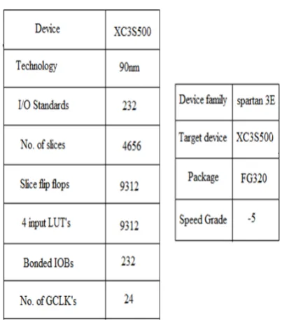
The main objective of this paper is to design and implementation of a fast multiplier, which can be used in any processor application. This paper deals with the study, design and implementation of various Multipliers. The work, study of Array Multiplication algorithm, Wallace Tree Multiplication algorithm and Booth Multiplication Algorithms has been explored and compared them by different criteria like Power, Time delay and Area. Architecture of these multiplier based on Power, speed and Area specification is designed here. Verification of functionally and analysis is done using Xilinx 10.1 Spartan3E (Family), XC3S500, FG320 (Package), -5 (Speed Grade) FPGA devices
2.1 Array Multiplier
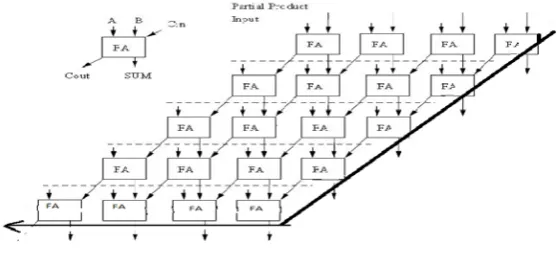
Array multiplier is organized by several stages of adders and AND-gates. It generates all the partial products after only one AND-gate delay. Then, it sums up all partial products sequentially. The advantage of this structure is that the arrangement of its adders is very regular and is favorable for layout. It also can be realized with parallel structure. However it occupies more area and hardware than that of iterative multiplier.
In Array Multiplier, consider two binary numbers A and B, of m and n bits. There are m n summands that are produced in parallel by a set of m n AND gates. n x n multiplier requires n (n-2) full adders, n half-adders and n2 AND gates. Also, in Array Multiplier worst case delay would be (2n+1) td.
Figure 1.1 4x4 bit Array Multiplier
2.2 Wallace Tree Multiplier
The Wallace tree multiplier is considerably faster than a simple array multiplier because its height is logarithmic in word size, not linear. However, in addition to the large number of adders required, the Wallace tree’s wiring is much less regular and more complicated. As a result, Wallace trees are often avoided by designers, while design complexity is a concern to them. Wallace tree styles use a log-depth tree network for reduction. Faster, but irregular, they trade ease of layout for speed. Wallace tree styles are generally avoided for low power applications, since excess of wiring is likely to consume extra power.
While subsequently faster than Carry-save structure for large bit multipliers, the Wallace tree multiplier has the disadvantage of being very irregular, which complicates the task of coming with an efficient layout. An example of 4-bit multiplication is shown in Fig.1.2. Let X(x3 x2 x1 x0) and Y(y3 y2 y1 y0) are two numbers multiplied by Wallace tree Multiplication Method.
2.3 Booth Multiplier
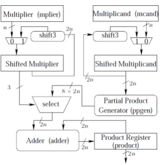
Traditional hardware multiplication is performed in the same way multiplication is done by hand: partial products are computed, shifted appropriately, and summed. This algorithm can be slow if there are many partial products (i.e. many bits) because the output must wait until each sum is performed. Booth’s algorithm cuts the number of required partial products in half. This increases the speed by reducing the total number of partial product sums that must take place.
Figure 1.2: 4x4 bit Wallace Tree Multiplier
Figure1.3: Booth Multiplier
To prove the functional correctness of the above design, we follow the technique explained in We illustrate the proof using the outline of the proof provided in that section. We use a simple Shift-and-Add multiplier as the reference TRS for multipliers. It performs multiplication by generating partial products. It shifts the multiplicand left by one bit after every partial product calculation. The partial product of the current stage is set to the sum of the previous partial product and the shifted multiplicand of the current stage or 0, depending on whether the multiplier bit corresponding to the current stage is 1 or 0. The Verilog code of the Shift-and-Add calls a shift and an add module iteratively.
3. Steps Performed to verification of functionality
3.1 Design Entry
The basic architecture of the system is designed in this step which is coded in a Hardware description Language like Verilog or VHDL. A design is described in Verilog using the concept of a design module.
Figure 1.4: Design Entry
3.2 Implement Design
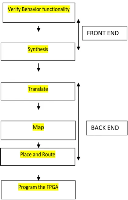
After synthesis, we run design implementation, which comprises the following steps:
Front End:-Verify and functionality are two main aspects of the coding and transforming the new encoded format.
Figure1.5:Flow Chart of Generating Programming file FRONT END
Verify Behavior functionality
Synthesis
Translate
BACK END Map
Place and Route
Program the FPGA
Back End:-
Translate - merges the incoming net lists and constraints into a Xilinx® design file.
Map - fits the design into the available resources on the target device, and optionally, places the design.
Place and Route - places and routes the design to the timing constraints.
Generate Programming File - creates a bitstream file that can be downloaded to the device.
3.3 Design Summary
The Design Summary allows you to quickly access design overview information, reports, and messages. By default, the Design Summary appears in the Workspace when you open a project, and it displays information specific to your targeted device and software tools. The panes on the left side of the Design Summary allow you to control the information displayed in the right pane.
Figure1.6 : Design Summary
3.4 Timing Simulation
In the timing simulation first we make the test bench and the set the value of timing constraints and simulate the test bench to verify the functionality of the design.
Figure 1.7: Timing Simulation
For the simulation of the multiplier we use software Xilinx tool.
Table 1-1: Summary of FPGA features
4. Results
4.1 Simulation Results of Array Multiplier
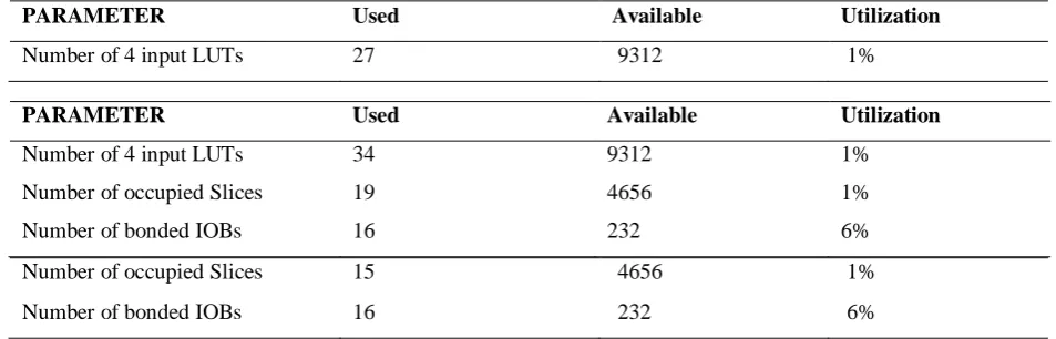
The simulation results of number of 4x4 bit Array Multiplier in terms of number of occupied slices, number of 4 input LUT and IOBs are shown in table.1-2.
Table 1.2: Xilinx Results for 4x4 bits Array Multiplier
PARAMETER Used Available Utilization
Number of 4 input LUTs 30 9312 1%
Number of occupied Slices 17 4656 1%
Number of bonded IOBs 16 232 6%
4.2 Simulation Results of Wallace Tree Multiplier
The simulation results of number of 4x4 bit, Wallace Tree Multiplier in terms of number of occupied slices, number of 4 input LUT and IOBs are shown in table.1-3.
Table 1.3: Xilinx Results for 4x4 bits Wallace Tree Multiplier
PARAMETER Used Available Utilization
Number of 4 input LUTs 27 9312 1%
Number of occupied Slices 15 4656 1%
Number of bonded IOBs 16 232 6%
4.3 Simulation Results of Booth Multiplier
The simulation results of number of 4x4 bit, Booth Multiplier in terms of number of occupied slices, number of 4 input LUT and IOBs are shown in table.1-4.
Table 1.4: Xilinx Results for 4x4 bits Booth Multiplier
5. Summary
Here the comparison of Array Multiplier, Wallace Tree Multiplier and Booth Multiplier have been discussed and analyzed.
PARAMETER Used Available Utilization
Number of 4 input LUTs 34 9312 1%
Number of occupied Slices 19 4656 1%
Number of bonded IOBs 16 232 6%
Table1.5: Comparison Summary for 4x4 bits multiplier
PARAMETER Array Multiplier Wallace Tree Multiplier Booth Multiplier
Number of 4 input LUTs 30 34 27
Number of occupied Slices 17 19 15
Time Delay(ns) 1.006
0.921
0.862
Cell Area 481 525 453
All the three Multipliers were employed in the same environment and following results has been obtained by using Xilinx Tool.The comparison summary for the 4*4 bits Array Multiplier, Wallace Tree Multiplier and Booth Multiplier. From table1.5 it can be observed that Booth Multiplier have small number of LUTs, Slices and less Time delay, Cell Area, and low power consumption. Wallace Tree Multiplier having less delay than Array Multiplier, but due to its higher complexity, its layout is complex
6. Conclusion
The designs of 4x4bits Array Multiplier, Wallace Tree Multiplier and Booth Multiplier have been implemented and analyzed on Spartan XC3S500E-5-FG320device using Xilinx tool.
After comparing all we came to a conclusion that Booth Multiplier is superior in respect like speed, delay, area. However Array Multiplier requires more number of components and large delay than Booth Multiplier. But the advantage of Array structure is that the arrangement of its adders is very regular and is favorable for layout. Wallace Tree Multiplier having less delay than Array Multiplier, but due to its higher complexity, its layout is complex.
Hence for small area requirement and for less delay requirement Booth’s Multiplieris suggested.
References
[1] S.Vaidya ,DDandekar, “DELAY-POWER PERFORMANCE COMPARISON OF MULTIPLIERS IN VLSI CIRCUIT DESIGN”, International Journal of Computer Networks & Communications (IJCNC), Vol.2, No.4, July 2010.
[2] R. Hussin, A.Yeon Md .Shakaff, N.Idris, Z.Sauli, Rizalafande C.Ismail, Afzan Kamarudin ,”An Efficient Modified Booth Multiplier Architecture”,IEEE International Conference on Electronics Design ,Dec. 2008.
[3] P.kumar G.Parate, Prafulla S. Patil, Dr (Mrs) S. Subbaraman ,“ASIC Implementation of 4 Bit Multipliers”,IEEE First International Conference on Emerging Trends in Engineering and Technology, pp. 408-413,2008.
[4] S R. Vaidya, D. R. Dandekar, “Performance Comparison of Multipliers for Power-Speed Trade-off in VLSI Design”, Recent Advances in Networking VLSI and Signal Processing, pp.262-265, June 2011. [5] A.Deshpande, Jeff Draper, “Squaring Units and a Comparison with Multipliers”, IEEE,
pp.1266-1269,2010.
[6] Y. Ben Asher, E. Stein” Extending Booth Algorithm to Multiplications of Three Numbers on FPGAs”,IEEE,pp.333-336,2008.
[7] A.Vazquez, E.Antelo, P.Montuschi,” Improved Design of High-Performance Parallel Decimal Multipliers”, IEEE TRANSACTIONS ON COMPUTERS, VOL. 59, NO. 5, pp.679-693, MAY 2010. [8] Dr. K.S. Gurumurthy, M.S. Prahalad,”Fast and Power Efficient 16 x16 Array of Array Multiplier using
Vedic Multiplication”,International Conference on Embedded System, Jan. 2011.
[9] S.Rong Kuang, J.Ping Wang , “Design of Power-Efficient Configurable Booth Multiplier “, IEEE TRANSACTIONS ON CIRCUITS AND SYSTEMS—I: REGULAR PAPERS, VOL. 57, NO. 3,pp.568-580 MARCH 2010.
[10] Qingzheng LI, Guixuan LIANG, Amine BERMAK, “A High-speed 32-bit Signed/Unsigned Pipelined Multiplier”, Fifth IEEE International Symposium on Electronic Design, Test & Applications ,pp. 207-211, 2010.
[11] B.Jose, D.Radhakrishnan ,”Fast Redundant Binary Partial Product Generators for Booth Multilication”, IEEE, pp.297-300,2007.
[12] X.Zhang, A.Bermak, F.Boussaid ,”Power Optimization in Multipliers Using Multi-Precision Combined with Voltage Scaling Techniques” ,IEEE ,pp. 79-82,2009.