ISSN : 2230-7109 (Online) | ISSN : 2230-9543 (Print)
Quantum Mechanical Properties of a Nano-Scale
p-n
Junction Based on Si/Si
0.4
Ge
0.6
/Si Quantum Well
1
Aritra Acharyya,
2Adrija Das,
3Kumari Alka Singh,
4Subhashri Chatterjee
1,2,3,4SKFGI, Sir J. C. Bose School of Engineering, Khan Road, Mankundu, Hooghly, West Bengal, India
Abstract
The quantum mechanical behavior of a reverse biased nano-scale p-n junction based on Si/Si0.4Ge0.6/Si quantum well has been studied by obtaining the self-consistent solution of coupled Schrödinger
and Poisson equations. The carrier confinement within the said
quantum well structure has been investigated by analyzing the special variations of electron and hole densities throughout the device structure obtained from the self-consistent solution of coupled Schrödinger and Poisson equations for different widths of the quantum well. The tunnel current across the junction has also been calculated for the heterostructure for different applied reverse bias voltages. Finally the current-voltage characteristics of the heterostructure under consideration have been investigated for different widths of the quantum well.
Keywords
Heterostructures, Poisson’s Equation, p-n Junction; Quantum Well, Schrödinger’s Equation
I. Introduction
The rapid advancements in epitaxial film growth techniques
such as Molecular Beam Epitaxy (MBE), Ultra-High Vacuum Chemical Vapor Deposition (UHV-CVD), Plasma-Etched Chemical Vapor Deposition (PE-CVD), etc. [1-4] have enabled ultra-thin structures to be grown with very sharp bandgap offsets [5-7] which leads to important quantum mechanical effects on
the device characteristics such as quantum confinement, quantum
tunneling of charge carriers [8-10]. The above mentioned quantum mechanical effects are strong motivations for studying the quantum mechanical behavior of some important heterostructures such as quantum well, multiquantum well, quantum wire, quantum
dot, etc. For an accurate description of carrier confinement and
tunneling effects on the device behavior, a fully self-consistent solution of the coupled Schrödinger and Poisson equations is required [11-13].
In the present paper, the quantum mechanical behavior of a reverse biased nano-scale p-n junction based on Si/Si0.4Ge0.6/Si quantum well has been studied by obtaining the self-consistent solution of coupled Schrödinger and Poisson equations subject to appropriate
boundary conditions. The carrier confinement within the said
quantum well structure has been investigated by analyzing the distributions of electron and hole concentrations throughout the device structure obtained from the self-consistent solution of coupled Schrödinger and Poisson equations for different widths of the quantum well. The tunnel current across the junction has been calculated by following the Kane’s model [14] for different applied
reverse bias voltages and finally the current-voltage characteristics
of the device structure under consideration have been investigated for different widths of the quantum well.
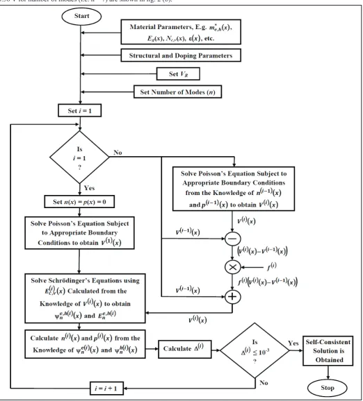
II. Self-Consistent Solution of Coupled Schrödinger-Poisson Equations
The Poisson’s equation relates the potential to the charge density distribution in the given semiconductor heterostructure system [15]. Thus, in order to determine the self-consistent potential
distribution in a given quantum heterostructure system, the one dimensional (1-D) Poisson’s equation must be solved. At the 1st iteration when both electron and hole concentrations (n(x) and p(x)) are unknown, the 1-D Poisson’s equation is solved numerically by using the 1-D Finite Difference Method (FDM) [16] subject to appropriate boundary conditions [15] assuming n(x) = p(x) = 0. The solution, i.e. the spatial variation of electrostatic potential (V( )1( )x ) can be obtained from it. Then the spatial variation of electrostatic potential (V( )1
( )
x ) is used to obtain thespatially varying minima of the conduction band and maxima of the valance band (Ec( )1
( )
x and Ev( )1( )
x ) which are used to solvethe 1-D Schrödinger’s equations numerically by using the forth order Runge-Kutta (RK4) method [17] to determine the eigen-energies ( e( )1
n
E , h( )1
n
E ) and corresponding wave functions (ψen( )1( )x , h( )( )x
n1
ψ ) in conduction and valance bands of the given quantum
heterostructure for a pre-specified number of modes (n). The wave
function solutions obtained in the 1st iteration ( e( )( )x n1
ψ , h( )( )x
n1
ψ ) are used in calculation of the electron and hole distributions (
( )( )x
n1 ,p( )1( )x ) in conduction and valance bands respectively. After
obtaining the electron and hole densities (n( )1( )x ,p( )1( )x ) at the
end of the 1st iteration, those are used to solve the Poisson’s equation to obtain V( )2
( )
x at the starting of the 2nd iteration. Againthe potential distribution obtained in the 2nd iteration (V( )2( )x ) is
used to calculate E( )( )x
c2 and Ev( )2( )x . Finally by solving the 1-D Schrödinger’s equations the electron and hole densities (n( )2( )x and
( )( )x
p2 ) at the end of 2nd iteration can be obtained which are used
as the inputs of the 3rd iteration. This process is repeated through iteration by iteration until the deviation (∆( )i ) associated with the solution of the potential distribution at (i–1)th iteration (V( )i−1( )x ) and ith iteration (V( )i( )x ) becomes smaller than a pre-specified value. The said deviation (∆( )i) at the end of the ith iteration may
be calculated as
( ) ( )
( )
( )( )
21 2 1 − = ∆ ∑ − x R i i i V x V x V (1)
If , then the self-consistent solution is assumed to be
achieved and the iterations are stopped. A detailed flowchart of
the self-consistent solution procedure of the coupled Schrödinger-Poisson equations for a given quantum heterostructure system
is shown in fig. 1. During each iteration (for i ≥ 2) the solution
of the Poisson’s equation (V( )i( )x) must be mixed with that in the
previous iteration (V( )i−1( )x) in order to ensure the convergence of the algorithm. If at ith iteration, V( )i( )x is simply fed back
into the Schrödinger’s equations via E( )i( )x
c and Ev( )i( )x, then the iteration process of calculating the wave function solutions, charge densities and resulting potential distribution has been shown not to converge [18]. The mixing of V( )i( )x and V( )i−1( )x at
the ith iteration is accomplished by implementing the extrapolated
convergence-factor method [18]. The equation representing the mixing algorithm is given by
( )
( )
x V( )( )
x f( ) ( )(
V( )
x V( )( )
x)
where the mixing fraction f( )i may be chosen between 0.05 and 0.10. For large value of f( )i the algorithm may run quickly but can
also diverge. If it is too small, then the convergence is slow. In the present work, the value of f( )i is chosen to be 0.05. It is also possible to varyf( )i from iteration to iteration [18]. The mixing algorithm is pictorially explained in fig. 1.
III. Numerical Results
The Si/Si1-xGex/Si heterostructure (x is the mole fraction of Ge) plays an important role in Si-based heterostructural technologies
including both bipolar and Field-Effect Transistor (FET) technologies. The significant application areas of such heterostructures in
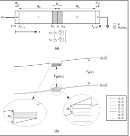
nano-scale electronic and opto-electronic devices inspired the author to study the quantum mechanical behavior of an n+-n-p-p+ heterostructure based on Si/Si1-xGex/Si quantum well under reverse bias. The mole fraction of Ge is chosen to be 60% in Si1-xGex alloy for the present study. The 1-D model of a reverse biased n+-n-p-p+ structure based on Si/Si
0.4Ge0.6/Si quantum well is shown in fig.
2 (a). Typical e n
E and h
n
E eigen-energy states within the well in both conduction and valance bands for applied reverse bias of VR =
0.50 V for number of modes (i.e. n = 7) are shown in fig. 2 (b).
ISSN : 2230-7109 (Online) | ISSN : 2230-9543 (Print)
Fig. 2(a): 1-D Model of the Reverse Biased n+-n-p-p+ structure
based on Si/Si0.4Ge0.6/Si Quantum Well Having Well Width of We = 50 Å and (b) corresponding energy-band diagram showing seven eigen-energy states within the well in both conduction and valance bands for applied reverse bias of VR = 0.50 V.
The structural and doping parameters of the n+-n-p-p+ structure
based on Si/Si0.4Ge0.6/Si quantum well under investigation are given in Table 1. The width of the quantum well has been varied between 10 and 100 Å to study the quantum mechanical behavior of the said structure under reverse bias. The material parameters
such as effective mass of charge carriers, electron affinity, effective
density of states in conduction and valance bands, permittivity, etc. of Si and Si0.4Ge0.6 at room temperature (i.e. at 300 K) are taken from recently published reports [19, 20] for the numerical calculations presented in this paper.
The wave function solutions are shown in figs. 3 and 4 for the
quantum well widths of 10 and 100 Å respectively for the applied reverse bias voltages of 0.5, 0.75 and 1.00 V. It is observed from
figs. 3 and 4 that, at smaller values reverse bias voltage, some of
the wave function solutions are localized within the boundaries of the quantum well. However, at larger values of reverse bias voltage, the said localizations of wave function solutions within
the boundaries of the quantum well are significantly reduced. It is noteworthy from figs. 3 and 4 that the number of wave function
solutions those are localized within the quantum well boundaries is larger for the quantum well structure having width of 100 Å as compared to its 10 Å counterpart for all applied reverse bias
voltages. Moreover, it is noted from the figures that, for each case,
the said localizations are more pronounced in conduction band than that in valance band. This is due to the greater depth of the
quantum well in conduction band (ΔEc = 0.1693 eV) than that in
valance band (ΔEv = 0.0770 eV) of the Si/Si0.4Ge0.6/Si quantum well structure.
Fig. 3: Spatial Variations of Wave Function Solutions Corresponding to the (a) – (c) Conduction Band and (d) – (f) Valance Band in the Reverse Biased n+-n-p-p+ structure based on Si/Si
0.4Ge0.6/Si
Quantum Well Structure Having 10 Å Quantum Well Width Under Different Reverse Bias Voltages
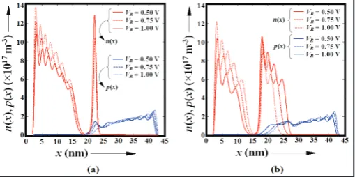
As the reverse bias voltage is increased, the Fermi level goes down higher in the surface of the quantum well at n-side while the same goes up in the surface of the quantum well at p-side. Thus more of the wave functions associated with the conduction band begin to penetrate into the Si layer in n-side; similarly more of the wave functions associated with the valance band begin to penetrate
into the Si layer in p-layer. As a consequence, a finite amount of
electrons and holes will tunnel quantum mechanically from the quantum well to n-type and p-type Si layers respectively. As the reverse bias voltage continues to increase, a larger percentage of
carriers find their way into the respective Si layers. This effect is illustrated in figs. 5 (a) and (b) where electron and hole densities
in the reverse biased n+-n-p-p+ structure based on Si/Si 0.4Ge0.6/
Si quantum well structure having 10 and 100 Å quantum well widths are plotted against distance as a function of the applied
reverse bias voltage. Larger percentage of carrier confinement is
observed within the quantum well having greater width (100 Å) for all reverse bias voltages, which is obvious. Again, due to the greater depth of the well in conduction band as compared to that
of valance band, the quantum confinement effect is found to be
more pronounced for electrons in conduction band as compared to that for holes in valance band; whereas quantum tunneling effect
is observed to be more significant for holes in valance band as
Table 1: Structural and Doping Parameters
Parameter Value
Wn (nm) 20.0
Wp (nm) 20.0
Wn+ (nm) 2.0
Wp+ (nm) 2.0
We (Å) 10.0 – 100.0
ND (×1023 m-3) 2.5
NA (×1023 m-3) 2.5
Nn+ (×1025 m-3) 1.0
Np+ (×1025 m-3) 1.0
The current-voltage characteristics of reverse biased n+-n-p-p+
heterostructure based on Si/Si0.4Ge0.6/Si quantum well having
quantum well widths of 10 and 100 Å are shown in fig. 6. It is observed from fig. 6 that the tunneling current increases sharply
with the increase of reverse bias voltage from 0.50 to 1.00 V. It is
noteworthy from the figure that the tunneling current is increased
in the Si/Si0.4Ge0.6/Si quantum well structure when the quantum well width of the same is increased. Thus the modulation of tunneling current may be achieved by varying the width of the quantum well.
Fig. 4: Spatial Variations of Wave Function Solutions Corresponding to the (a) – (c) Conduction Band and (d) – (f) Valance Band in the Reverse biased n+-n-p-p+ structure based on Si/Si
0.4Ge0.6/Si
Quantum Well Structure Having 100 Å Quantum Well Width Under Different Reverse Bias Voltages
Fig. 5: Spatial Variations of Electron and Hole Densities in the Reverse Biased n+-n-p-p+ structure based on Si/Si
0.4Ge0.6/Si
quantum well structure having (a) 10 Å and (b) 100 Å quantum Well Widths Under Different Reverse Bias Voltages
IV. Conclusion
The quantum mechanical behavior of a reverse biased nano-scale p-n junction based on Si/Si0.4Ge0.6/Si quantum well has been studied by obtaining the self-consistent solution of coupled Schrödinger and Poisson equations via a simple algorithm presented in this
paper. The carrier confinement within the said quantum well
structure has been investigated by analyzing the special variations of electron and hole densities throughout the device structure obtained from the self-consistent solution of coupled Schrödinger and Poisson equations for different widths of the quantum well. The tunnel current across the junction has also been calculated for the heterostructure for different applied reverse bias voltages. Results show that, due to the greater depth of the quantum well in conduction band as compared to that in valance band of Si/
Si0.4Ge0.6/Si heterostructure, the quantum confinement effect is
more pronounced for electrons in conduction band as compared to that for holes in valance band; whereas quantum tunneling effect
is more significant for holes in valance band than that for electrons
in conduction band. Finally the current-voltage characteristics of the heterostructure under consideration have been investigated for different widths of the quantum well. It is observed that the modulation of tunneling current may be achieved by varying the width of the quantum well.
References
[1] Casey, H. C., Cho, A. Y., Barnes, P. A.,“Application of molecular-beam epitaxial layers to heterostructure laser”, IEEE Journal of Quantum Electronics, Vol. 11, Issue 7, 1975, pp. 467-470.
[2] Kasper, E., Luy, J. F.,“Molecular beam epitaxy of silicon based electronic structures”, Microelectronics Journal, Vol. 22, Issue 3, 1991, pp. 5-16.
[3] Luo, G., Zhu, P., Chen, P., Liu, Z., Lin, H., Qian, P., “An ultrahigh vacuum chemical vapor deposition system and its application to growth of nMOSFET and HBT structures”, Vacuum, Vol. 59, Issue 4, 2000, pp. 927-931.
[4] Holmes, M. R., Liu, S., Keeley, J., Jenkins, M., Leake, K., Schmidt, H. Hawkins, A. R.,“Hollow Waveguides with Low Intrinsic Photoluminescence Fabricated with PECVD Silicon Nitride and Silicon Dioxide Films”, IEEE Photonics Technology Letters, Vol. 23, 2011, pp. 1466-1488.
[5] McKay, K. S., Lu, F. P., Kim, J., Yi, C., Brown, A. S., Hawkins, A. R.,“Band discontinuity measurements of the wafer bonded InGaAs/Si heterojunction”, Applied Physics Letters, Vol. 90, 2007, pp. 222111.
[6] Wu, W., Hawkins, A. R., Bowers, J. E.,“Design of Silicon Hetero-Interface Photodetectors”, Journal of Lightwave Technology, Vol. 15, No. 8, 1997, pp. 1608-1615.
[7] Hawkins, A. R., Reynolds, T. E., England, D. R., Babic, D. I., Mondry, M. J., Streubel, K., Bowers, J. E.,“Silicon Heterointerface Photodetector”, Applied Physics Letters, Vol. 68, No. 26, 1996, pp. 3692-3694.
[8] Bean, J. C.,“Silicon-based semiconductor heterostructures: column IV bandgap engineering”, Proceedings of the IEEE, Vol. 80, Issue 4, 1992, pp. 571-587.
[9] Ravaioli, U. et al.,“Numerical simulation of electron
confinement in contiguous quantum wires”, Supperlattices
and Microstructures, Vol. 11, Issue 3, 1992, pp. 343-345. [10] Borukhovich, A. S.,“Quantum tunneling in multilayers
ISSN : 2230-7109 (Online) | ISSN : 2230-9543 (Print)
[11] Blatt, J. M.,“Practical points concerning the solution of the Schrödinger equation”, Journal of Computational Physics, Vol. 1, Issue 3, 1967, pp. 382-396.
[12] Luscombe, J. H. et al.,“Electron confinement in quantum
nanostructures: Self-consistent Poisson-Schrödinger theory”, Physical Review B, Vol. 46, No. 16, 1992, pp. 10262-10268.
[13] Wang, L. et al.,“Self-consistent 1-D Schrödinger–Poisson solver for III–V heterostructures accounting for conduction band non-parabolicity”, Solid-State Electronics, Vol. 54, Issue 11, 2010, pp. 1257-1262.
[14] Kane, E. O.,“Theory of Tunneling”, Journal of Applied Physics, Vol. 32, 1961, pp. 83-91.
[15] Acharyya, A., Chatterjee, S., Das, A., Singh, K. A., “Self-Consistent Solution of Schrödinger-Poisson Equations in a Reverse Biased Nano-Scale p-n Junction Based on Si/ Si0.4Ge0.6/Si Quantum Well”, Journal of Computational Electronics, 2014.
[16] Doudlas, J., Yuan, Y.,“Finite difference method for the transient behavior of a semiconductor device”, IMA preprint Series # 286, pp. 1-20, 1987.
[17] Christodoulou, N. S.,“An algorithm using Runge-Kutta methods of orders 4 and 5 for systems of ODEs”, International Journal of Numerical Methods and Applications, Vol. 2, No. 1, 2009, pp. 47-57.
[18] Stern, F.,“Iteration methods for calculating self-consistent fields in semiconductor inversion layers”, Journal of Computational Physics, Vol. 6, Issue 1, 1970, pp. 56-67. [19] Ku, J. H., Nemanich, R. J.,“Surface electronic structure of
clean and hydrogen-chemisorbed SixGe1-x alloy surfaces”, Physical Review B, Vol. 54, No. 19, 1996, pp. 102-110. [20] “Electronic Archive: New Semiconductor Materials,