Global Journal of Advanced Engineering Technologies and Sciences
IMPLEMENTATION OF 16 BIT RISC PROCESSOR USING VHDL
MR. AVINASH PAWAR*, PROF.SUMIT S.DHAMAL
*Dept.of Instrumentation, VPM’S Maharshi Parshuram College of Engineering, Velneshwar, K.K.Wagh
College of Engineering & Research, Nashik.
Abstract
Study over the years has shown that simple instruction are used most of the time in CISC ( Complex Instruction Set Computing ) processors and many complex instructions can be replaced by group of simple instructions. In that sense RISC (Reduced Instruction Set Computing) processor are designed to execute very few simple instructions. They operate on data which is mostly present in internal registers. Most of the RISC processors use hardwired control approach which simplifies design process. External memory is accessed by LOAD and STORE instructions. RISC processor supports only few addressing modes and most of them are register based.
Pipelining is used to improve the throughput of the processor by dividing the instruction execution in stages. Although single instruction takes same time for execution as in sequential execution, parallel operations on instructions in different stages reduces the overall time of execution. The balance of work between different stages of pipelining is important as the slowest stage of the pipeline decides the throughput of the processor. The consequences of pipelining are the structural hazards, data hazards and control hazards. They can be handled using the methods of forwarding, stalling and flushing. Stalling degrades the performance by delaying the instruction execution. Prefetching unit is designed which works as a small cache. It is used to prefetch the instructions from memory and stored them inside the buffer.
Developed RISC processor handles the hardware interrupts and exceptions. RESET has been assigned the highest priority. Six external hardware interrupts are available and are vectored. Overflow and undefined instruction exceptions are also dealt with.
VHDL has been used for modeling the processor. Xilinx ISE 9.2i is used for simulation, synthesis and physical implementation. Hierarchical approach is used for modeling the RISC processor. Basic units are described using behavioral programming and they are interconnected using structural programming to form complete RISC processor..
Keywords: RISC processor, CISC processor, VHDL.
Introduction
There are two design philosophies of microprocessor: Complex Instruction Set Computers (CISC) and Reduced Instruction Set Computers (RISC). In this introductory chapter these two trends are briefly explained. The objectives of this work are stated and then the “organization of dissertation” is presented.
Complex Instruction Set Computer (CISC)
Fig. 1 CISC Implementation
The implementation of CISC processor includes microprogrammed control. The conceptual diagram is shown in fig. 1. A microprogram is a small run-time interpreter that takes the complex instruction and generates a sequence of simple instructions that can be executed by hardware. This was used to eliminate the semantic gap between high-level language statements and the instructions of processor. Hence most CISC designs use microprogrammed control [1].
Reduced Instruction Set Computer (RISC)
RISC (Reduced Instruction Set Computer) processors have gained significant attention of designers from last few years because of many features of it. Survey by program analysts over the years has shown that most of the time simple instructions are used and complex instructions are used occasionally. It is also found that many complex instructions can be replaced by group of simple instructions. Thus it is beneficial to design a system that supports a few simple data types efficiently and from which the missing complex data types can be synthesized.
RISC processors have larger register set than CISC processors to avoid the frequent use of external memory. Most of the instructions operate on operand present in internal registers. This aspect improves the performance of the processor.
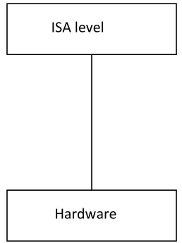
RISC designs eliminate the microprogram layer and use the hardware to directly execute instructions. RISC implementation is shown in figure 2.
Fig. 2 RISC Implementation
Features of the RISC Processors
1) Simple Instructions. The objective is to design simple instructions so that each can execute in one clock cycle. This is possible through pipelined architecture. The advantage of simple instruction is that all operations can be hardwired.
ISA level
Microprogram Control
Hardware
ISA level
2) Register-to-Register Operations. Most of the operations are carried out on the data present in internal registers rather than external memory. This simplifies instruction set design and the structure of control unit.
3) Simple Addressing Modes. Simple addressing modes allow fast address computation of operands. Most instructions use register based addressing. Only load and store instructions need a memory addressing mode.
4) Large Number of Registers. For register based operations we need large number of register to optimize the design. But the fixed length of instruction put limit on the registers that can be designed for the processor.
5) Fixed-Length, Simple Instruction Format. Variable length instructions can cause implementation and execution inefficiencies. Hence fixed length format is used. The RISC processor also uses simple instruction format where boundaries of various fields in an instruction such as opcode, source and destination operands are fixed. This allows an efficient decoding and scheduling of instructions.
6) Pipelining. The method of pipelining is used to speed-up execution. The problems arising due to pipelining are also handled.
VHDL (Very high speed integrated circuit Hardware Description Language) is used as a programming language to implement the proposed processor. There are several reasons to choose VHDL to implement design:-
1. Through the use of structural modeling, VHDL can describe how a system is composed of smaller systems and the connections between them.
2. Behavioral modeling allows a system’s functionality to be described using common programming language.
Overview of RISC Processor Architecture
To improve the throughput of processor, the pipelined architecture is used. Execution of the instruction is divided into four stages viz.
1. Stage1- Instruction Fetch Stage. 2. Stage2- Instruction Decode Stage. 3. Stage3- Instruction Execution Stage. 4. Stage4- Memory/IO-Write Back Stage.
Every instruction proceeds to the next stage in each clock cycle and new instruction enters the instruction fetch stage. Each individual instruction takes four clock cycles for complete execution after entering the instruction fetch stage provided that no stalls occur.
Control unit generate necessary signal at appropriate time for all the stages for instruction execution. Branch forwarding unit flushes the instructions behind branching instruction in the pipeline if branching is going to occur. Execution forwarding unit takes care of data hazard by forwarding the result of previous instruction to execution stage if data hazard occurs. Prefetching unit prefetches instruction from memory when processor is not utilizing external memory. It stores the prefetched instructions in prefetch queue, which is four words deep. Hazard detection unit is used to detect whether conflicts are going to occur and generate the necessary signals for other units [8]. Interrupt and exception unit handles the external interrupts and exceptions generated internal to the processor. The fig.3 shows the architecture of RISC processor implemented in the design.
Pipelined Stages of RISC Processor
Four stages of the RISC processor pipeline are described below.
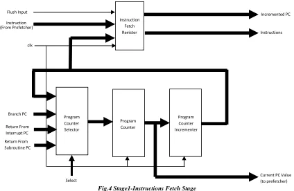
Stage1-Instruction Fetch Stage
This stage consists of program counter, program counter incrementer and selector, which select the new value of program counter. This unit is responsible for obtaining the instruction from memory through prefetcher. The block diagram of instruction fetch stage is shown in fig. 4.
Fig. 3 RISC Processor Block Diagram
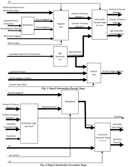
Stage2-Instruction Decode Stage Register
This is used to store the output produced by instruction decode stage. It stores mainly content of source register 1 and source register 2, sign extended immediate data.
Fig.4 Stage1-Instructions Fetch Stage
Stage3-Instruction Execution Stage
Interrupt Unit Stage 2 Instruction Decode Stage Stage 3 Instruction Execution Stage Stage 4 Memory/IO Write Back Stage Control Unit Hazard Detection Unit Stage 1 Instruction Fetch Stage Forwarding Unit Prefetch Unit Memory Read Write Control Input Port Interrupt Input Interrupt Acknowledgement Output Port Address Lines Data Lines
stage consist of arithmetic logic unit (ALU), instruction execution stage register and multiplexer.
Arithmetic logic unit carries out arithmetical operations like addition and subtraction, logical operations like AND, OR, XOR, NOR and NOT, arithmetical and logical shifts.
Fig. 5 Stage2-Instruction Decode Stage
Fig. 6 Stage3-Instruction Execution Stage
Register File Multiplexer Sign Extension Unit Branch Unit Instruction Decode Stage Register Write Back Result From
Write Back Stage
Operand Part of Instruction
Write Back Register Read Register Selector
Source Register 1
Source Register 2
Content of Source Register 1
Content of Source Register 2
Sign Extended Immediate Data Immediate Data Part of Instruction
Write Enable
Current PC Value
Branch Register Content
Branch Type Select
Branch Target Address Sign Extended Immediate Data Content of Source
Register 1
Content of Source Register 2 clk Arithmetic Logic Unit (ALU) Multiplexer Instruction Execution Stage Register clk JAL Control PC Operation Extended Immediate Data Content of Source
Register 1
Content of Source Register 2
Result from ALU Decode Stage PC
Result Execution
Stage Result
Execution Stage PC
Design And Implementation Of Risc Processor
VHDL is a language for describing digital electronics system which is used as design tool in this dissertation. Hierarchical approach has been used for designing the RISC processor. After designing the RISC processor and simulating the result.This chapter begins with brief introduction of VHDL language. Next to it basic programming technique are explained. Then emphasis is given on some terminologies in VHDL.
VHDL
VHDL is an acronym which stands for VHSIC (Very High Speed Integrated Circuits) Hardware Description Language. VHDL is designed to fill a number of needs in the design process. First, it allows description of the structure of a system, that is, how it is decomposed into subsystems and how those subsystems are interconnected. Second, it allows the specification of the function of a system using familiar programming language forms. Third, as a result, it allows the design of a system to be simulated before being manufactured, so that designers can quickly compare alternatives and test for correctness without the delay and expense of hardware prototyping. Fourth, it allows the detailed structure of a design to be synthesized from a more abstract specification, allowing designers to concentrate on more strategic design decisions and reducing time to market [12].
VHDL is being used for documentation, verification and synthesis of large digital designs. This is actually one of the key features of VHDL, since the same VHDL code can theoretically achieve all three of these goals, thus saving a lot of effort. In addition to being used for each of these purposes, VHDL can be used to take three different approaches to describing hardware. These three different approaches are the structural, data flow and behavioral methods of hardware description. Most of the time a mixture of the three methods is employed. The following sections introduce you to the language by examining its use for each of these three methodologies. [13].
VHDL was established as the IEEE 1076 standard in 1087. In 1993, the IEEE 1076 standard was updated and an additional standard, IEEE 1164 was adopted. In 1996, IEEE 1076.3 became the VHDL synthesis standard [13].
Results And Discussion
Basic entities have been programmed using behavioral model and they are used as components to form the different units of RISC processor. These units in term are used as components for building the RISC processor using structural programming. The simulation results for different unit and final RISC processor are shown below.
Simulation results for stage1 shown in fig, 7. Based on value of selection input (OPC) generated by control unit for instruction in execution stage, next program counter value (pcValue) is decided. As shown in simulation if OPC= 0000B, then the old content of the pc Value is incremented by one. The old content of pc Value in simulation result is 1000H, and the pc Value incremented by one is 1001H. If OPC= 0100B, then the overflow operation is selected, and the pc Value incremented by one. The old content of pc Value in simulation result is 2001H, and the pc Value incremented by one is 0000H. Instruction from prefetch unit at address specified in program counter is taken and is forwarded to next stage. If flush input is high, instruction fetch stage register is flushed out.
Simulation results for stage2 are shown in fig. 8. This stage decides the combination of read registers based on reg Select input. Input rf_enable is used for enabling the write operation in register file. If branch instruction is there in execution stage, then type of branching (absolute or relative) is decided by branch_select input. The contents of read registers are forwarded to next stage.
Simulation results for stage3 are shown in fig.9. The ex_select input activated one of the components out of basic ALU, shift unit and move immediate unit. The input alu_function decides the operation to be carried out on the data at input. Contents of source registers and sign extended immediate data are input to this stage. The result and the code for write back register are forwarded to next stage.
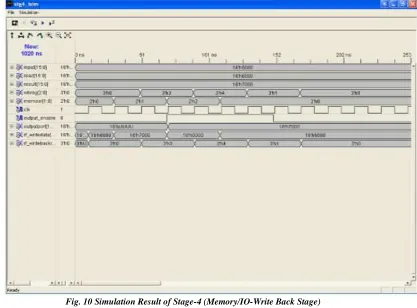
Simulation results for stage4 are shown in fig. 10. The input memSel is used to select from data on input port, data read from memory and result of execution stage as final result to be written back into destination. When output_enable is high, the result is placed on the output port. Final result and code for write-back register are output from this stage.
not distributed properly over different stages of pipeline, performance degrades because the slowest stage decides the throughput of the pipeline. Maintaining the sequence in the working of the pipeline is also one of the important points to consider while designing stages of pipeline.
Hardwired approach is used in this design because instructions are very few, simple operations are to be carried out on the data, instruction length is fixed and hence less number of control signals need to be generated for all the instructions. Clock signal is used as the basis for generating control signals in sequence for all the pipelined stages and other units of processor.
Structural hazards, data hazards and control hazards are resolved using hazard detection unit, execution forwarding unit and branch forwarding unit. An instruction called JAL and RJAL has been designed equivalent to CALL and RETURN with the difference that the return address is saved in one of the register rather than external memory. Only LOAD and STORE instructions access the external memory. All other instructions operate on a data present in internal registers or immediate data present in the instruction itself.nit and branch forwarding unit. An instruction called JAL and RJAL has been designed equivalent to CALL and RETURN with the difference that the return address is saved in one of the register rather than external memory. Only LOAD and STORE instructions access the external memory. All other instructions operate on a data present in internal registers or immediate data present in the instruction itself.
Fig. 11 Simulation Result of Control Unit
Conclusion
Through pipelining, the maximum through put of execution is achieved as one instruction per clock pulse provided that there are no stalls. This is possible due to hardwired approach for design of control unit and fixed length instruction format. To resolve resource conflicts, result forwarding is efficient than stalling as it remove the penalty of time in handling such conflicts. The prefetch unit is used for handling the structural hazards while flushing is used to handle control hazards. The prefetch buffer is like small cache and not works on FIFO principle. The design is simulated and then implemented on FPGA successfully. The maximum frequency of operation on the Xilinx’s Spartan-II FPGA is 26-MHz.
The emphasis is placed on only implementing the common features of RISC processor in this work. Other aspects like device utilization on FPGA, power consumption can be taken into consideration and methods can be found out for their minimization. The work can be extended to Development of a 32-bit RISC processor having the features like protection for data, support for virtual memory etc..
1.Development of separate hardware for memory.
2.Development of full cache memory subsystem inside the processor. 3.Implementation of branch prediction logic.
References
1. Sivarama P. Dandamudi, “Fundamentals of Computer Organization and Design”, Springer-Verlog, New York, Inc., 2003.
2. John L. Hennessy and David A. Patterson, “Computer Architecture a Quantitative Approach”, 3rd Edition,
Morgan Kaufmann Publishers, Inc., 2000.
3. William Stallings, “Computer Organization and Architecture: Designing for Performance”, New Delhi: Prentice Hall of India, 2000.
4. Morris M. Mano, “Computer System Architecture”, New Delhi : Prentice Hall of India, 1989.
5. Smyth N., McLoone M. and McCanny J.V., “Reconfigurable Cryptographic RISC Microprocessor”, VLSI Design, Automation and Test, 2005. (VLSI-TSA-DAT). 2005 IEEE VLSI-TSA International Symposium, pp. 29-32.
6. Wicks J.A., Jr. and Martin H.L., “Design of a Fault-Tolerant RISC Microprocessor Using VHDL”, System Theory, 1991, Proceedings, Twenty-Third Southeastern Symposium, pp. 354-358.
7. Dolle M. and Schlett M., “A Cost-Effective RISC/DSP Microprocessor for Embedded Systems”, Micro, IEEE, 1995, pp. 32-40.
8. Seung Ho Lee, Beoyng Yoon Choi and Moon Key Lee, “ASIC Implementation of a RISC Microprocessor for Portable Workstation”, TENCON '95. 1995 IEEE Region 10 th International Conference on
Microelectronics and VLSI, pp. 484-487.Bailey D.H., “RISC Microprocessors and Scientific computing”, Supercomputing ' 93. Proceedings, IEEE, 1993, pp. 645-654.
9. Choquette J., Gupta M., McCarthy D. and Veenstra J., “High Performance RISC Microprocessors”, Micro, IEEE, 1999, pp. 48-55.
10. Peter J. Ashenden, “The Designer’s Guide to VHDL”, 2nd Edition, Morgan Kaufmann Publishers, 2003.
11. J.Bhaskar, “VHDL Primer”, 3rd Edition, Pearson Education Asia, 2001.
12. Ben Cohen, Kluwer, “VHDL Coding Styles and Methodologies”, 2nd Edition,