R E S E A R C H
Open Access
High-performance hardware architectures for
multi-level lifting-based discrete wavelet
transform
Anand D Darji
1*, Shailendra Singh Kushwah
2, Shabbir N Merchant
1and Arun N Chandorkar
1Abstract
In this paper, three hardware efficient architectures to perform multi-level 2-D discrete wavelet transform (DWT) using lifting (5, 3) and (9, 7) filters are presented. They are classified as folded multi-level architecture (FMA), pipelined multi-level architecture (PMA), and recursive multi-level architecture (RMA). Efficient FMA is proposed using dual-input Z-scan block (B1) with 100% hardware utilization efficiency (HUE). Modular PMA is proposed with the help of block (B1) and dual-input raster scan block (B2) with 60% to 75% HUE. BlockB1andB2are micro-pipelined to achieve critical path as single adder and single multiplier for lifting (5, 3) and (9, 7) filters, respectively. The clock gating technique is used in PMA to save power and area. Hardware-efficient RMA is proposed with the help of block (B1) and single-input recursive block (B3). Block (B3) uses only single processing element to compute both predict and update; thus, 50% multipliers and adders are saved. Dual-input per clock cycle minimizes total frame computing cycles, latency, and on-chip line buffers. PMA for five-level 2-D wavelet decomposition is synthesized using Xilinx ISE 10.1 for Virtex-5 XC5VLX110T field-programmable gate array (FPGA) target device (Xilinx, Inc., San Jose, CA, USA). The proposed PMA is very much efficient in terms of operating frequency due to pipelining. Moreover, this approach reduces and totals computing cycles significantly as compared to the existing multi-level architectures. RMA for three-level 2-D wavelet decomposition is synthesized using Xilinx ISE 10.1 for Virtex-4 VFX100 FPGA target device.
Keywords: Clock gating; DWT; Dual-scan architecture; Folding; FPGA; Lifting
1 Introduction
In recent years, multi-level two-dimensional discrete wavelet transform (2-D DWT) is used in many applica-tions, such as image and video compression (JPEG 2000 and MPEG-4), implantable neuroprosthetics, biometrics, image processing, and signal analysis. due to good energy compaction in higher-level DWT coefficients. To meet application constraint such as speed, power, and area, there is a huge demand of hardware-efficient VLSI archi-tectures in recent years. DWT provides high compres-sion ratio without any blocking artifact that deprives reconstructed image of desired smoothness and continu-ity. However, implementation of convolution-based DWT
*Correspondence: [email protected]
1Department of Electrical Engineering, Indian Institute of Technology Bombay, Powai, Mumbai 400076, India
Full list of author information is available at the end of the article
has many practical obstacles, such as higher computa-tional complexity and more memory requirement. There-fore, Swelden et al. [1] proposed lifting wavelet, which is also known as second-generation wavelet. DWT can be implemented using convolution scheme as well as lift-ing scheme. The computational complexity and memory requirement of lifting scheme is very less as compared to convolution. Several architectures have been proposed to perform lifting-based DWT, which differ in terms of numbers of multipliers, adders, register, line buffers requirement, and scanning scheme adopted. 2-D DWT can be computed by applying 1-D DWT row-wise, which produces low-frequency (L) and high-frequency (H) sub-bands and then process these sub-sub-bands column-wise to compute one approximate (LL) and three detail (LH, HL, HH) coefficients.
Jou et al. have proposed architecture with straightfor-ward implementation of the lifting steps and therefore this
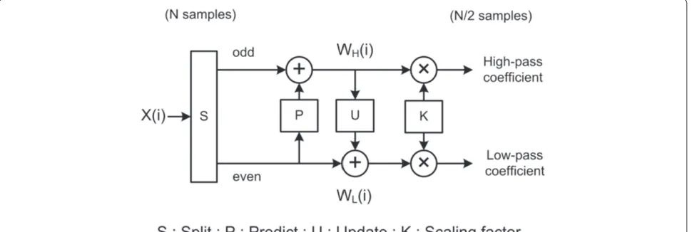
Figure 1Lifting scheme [11].
architecture has long critical path [2]. An efficient pipeline architecture having critical path of only one multiplier has been proposed by merging predict and update stages by Wu and Lin [3]. Lai et al. have implemented dual-scan 2-D DWT design based on the algorithm proposed by Wu et al. with critical path delay of one multiplier and throughput of 2-input/2-output at the cost of more pipeline registers [4]. Dual-scan architecture with one
multiplier as a critical path has also been proposed by Zhang et al. at the cost of complex control path [5]. Hsia et al. [6] have proposed a memory-efficient dual-scan
2-D lifting 2-DWT architecture with temporal buffer 4Nand
critical path of two multipliers and four adders. Recently, a dual-scan parallel flipping architecture is introduced with the critical path of one multiplier, less pipeline registers, and simple control path [7].
Figure 3Dual-input raster scanning technique.
Several lifting-based 2-D DWT multi-level architec-tures have been suggested for efficient VLSI implementa-tion [3,8-15] that take into consideraimplementa-tion various aspects like memory, power, and speed. These architectures can be classified as folded architectures [8], parallel archi-tectures [14], and recursive archiarchi-tectures [16]. Andra et al. [8] proposed simple folded architecture to perform several stages of 2-D DWT with the help of memory. Systolic architecture is proposed by Huang et al. [9] for a DWT filter with finite length. Multi-level 2-D DWT decomposition is implemented by recursive architecture (RA) [10,16], but these approaches demand large amount of frame buffers to store the intermediate LL output and also require complex control path. Wu and Lin [3] pro-posed folded scheme, where multi-level DWT computa-tion is performed level by level, with memory and single processing element. Unlike RA, folded architecture uses simple control circuitry, and it has 100% hardware uti-lization efficiency (HUE). Folded architectures consist of memory and a pair of 1-D DWT modules, a row pro-cessing unit (RPU) and a column propro-cessing unit (CPU). Mohanty and Meher [12] proposed a multi-level archi-tecture for high throughput with more number of adders and multipliers. Xiong et al. [13] proposed two line-based high-speed architectures by employing parallel and
pipelining techniques, which can performj-level
decom-position forN×Nimage in approximate 2(1−4−j)N2/3
and(1−4−j)N2/3 clock cycles. Hsia et al. [17] have
pro-posed a symmetric mask-based scheme to compute 2-D integer lifting DWT, where the separate mask is used for each sub-band. Mask-based algorithms do not require temporal buffers, but they are not suitable for area effi-cient implementation due to a large number of adder and multiplier requirement. A memory efficient archi-tecture is proposed by Lai et al. [4] with low latency. Al-Sulaifanie et al. [18] designed an architecture, which is independent of input image size with moderate speed and HUE. Recently, Aziz and Pham [15] have proposed par-allel architecture for lifting (5, 3) multi-level 2-D DWT with a single processing unit to calculate both predict
and update values. But this architecture requires 4Nline
buffers for single-level decomposition and has less HUE due to the wastage of the alternate clock cycle. Memory management is key to design multi-level 2-D DWT archi-tectures. The lifting-based multi-level 2-D DWT architec-ture is suggested using overlapped stripe-based scanning method [19].
Three types of memory buffer are generally used in any 2-D DWT architecture, i.e., frame, transposition, and temporal memory. Frame memory is required to
Figure 5Hardwired scaling unit (HSU).(a)α=1/2.(b)α=1/4.
store intermediate LL coefficients, transposition mem-ory is mainly required for storing row processor out-put, and temporal memory is required to store partial results during column processing. Temporal and transpo-sition memories are on-chip, while the frame memory is on or off-chip, depending upon the architecture. Size of transposition memory is limited by the method adopted to scan external memory. Different scanning techniques have been proposed, such as line-based, block-based, and stripe-based [14,19-21].
This paper is organized as follows. Section 2 pro-vides a brief overview of lifting scheme. In Section 3, design of three efficient multi-level architectures and their modules are discussed. Performance comparison, field-programmable gate array (FPGA) implementation and timing analysis are described in Section 4. Conclusions are presented in Section 5.
2 Lifting scheme
The lifting scheme is a hardware-efficient technique to perform DWT. Lifting scheme entirely relies on spatial domain and it has many advantages as compared to the convolution method of calculating DWT such as in-place
Table 1 Data flow of predict/update module
Clock Input D1 D2 P/U
1 X1,1:X1,3:X1,2
2 X1,3:X1,5:X1,4 X1,1+X1,3 X1,2
3 X1,5:X1,7:X1,6 X1,3+X1,5 X1,4 P/U1,1
4 X1,7:X1,9:X1,8 X1,5+X1,7 X1,6 P/U1,2
computation, symmetric forward and inverse transforms, and perfect reconstruction. The basic principle of lifting scheme is to factorize the polyphase matrix of a wavelet filter into a sequence of alternating upper and lower trian-gular matrices and a diagonal matrix and convert the filter implementation into banded matrices multiplications [1] as shown by (1) and (2). Where, he(z) and ge(z) (ho(z)
andgo(z)) represent the even parts (odd part) of the
low-pass and high-low-pass filters, respectively.si(z)andti(z)are
denoted as predict lifting and update lifting polynomials.
K and 1/Kare scale normalization factors. Factorization
of classical wavelet filter into lifting steps reduces the computational complexity up to 50%.
P(z)=
he(z)ho(z)
ge(z)go(z)
(1)
P(z)=
m
i=1
1 si(z)
0 1
1 0
ti(z) 1
K 0
0 1/K
(2)
Every reconstructible filter bank can be expressed in terms of lifting steps in general. Figure 1 shows a block diagram of a forward lifting scheme to compute 1-D DWT. It is composed of three stages: split, predict, and update. In split stage, input sequence is divided into two subsets, an even indexed sequence and an odd indexed sequence. During the second stage, the even indexed sequence is used to predict odd sequence. Two
consec-utive even and one odd indexed input sequences X(i)
are used to calculate high-pass coefficient WH(i) (detail
Figure 6Dual-input Z-scan block (B1) for lifting (5, 3) filter.
input sequence are used to calculate low-pass coefficients WL(i)(approximate coefficients), as given by (4).
WH(i)=X(2i−1)+α[X(2i)+X(2i−2)] (3)
WL(i)=X(2i−2)+β[WH(i)+WH(i−1)] (4)
3 Proposed architectures
In this section, the proposed dual-input Z-scan
architec-ture (B1), dual-input raster scan module (B2), and
single-input blockB3are discussed. All these blocks are designed
with consideration of lifting wavelet to perform
single-level 2-D DWT. BlocksB1 andB2 are designed to
pro-cess two inputs and generate two outputs at every clock cycle. The total clock cycles required to perform one-level
decomposition of aN×Nimage isN2/2 without
consider-ing latency. Then, three novel architectures for multi-level
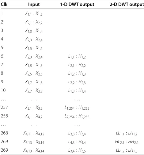
Table 2 Data flow of block (B1): image size 256×256
Clk Input 1-D DWT output 2-D DWT output
1 X1,1:X1,2
2 X2,1:X2,2
3 X1,3:X1,4
4 X2,3:X2,4
5 X1,5:X1,6
6 X2,3:X2,4 L1,1:H1,2
7 X1,5:X1,6 L2,1:H2,2
8 X2,5:X2,6 L1,2:H1,3
9 X1,7:X1,8 L2,2:H2,3
10 X2,7:X2,8 L1,3:H1,4
. . . . . . . . .
257 X3,1:X3,2 L1,254:H1,255
258 X4,1:X4,2 L2,254:H2,255
. . . . . . . . .
268 X4,11:X4,12 L3,3:H3,4 LL1,1:LH1,2
269 X3,13:X3,14 L4,3:H4,4 HL2,1:HH2,2
269 X4,13:X4,14 L3,4:H3,5 LL1,2:LH1,3
2-D DWT are presented, i.e., folded multi-level archi-tecture (FMA), pipelined multi-level archiarchi-tecture (PMA), and recursive multi-level architecture (RMA). The FMA
is composed of a block (B1) andN2/4 off-chip memory,
where as the PMA is composed of a block (B1) to
per-form first-level decomposition and block (B2) for higher
levels of decompositions. The RMA is composed of block
(B1) and block (B3) to compute first-level and higher-level
decomposition.
Three different architectures are suggested based on different VLSI optimization criteria such as area, power, speed, throughput, and memory. FMA is a straight for-ward design which requires simple control but has lower
throughput and it demands N2/4 memory. PMA is
designed to satisfy the need of high throughput at the cost of area, whereas RMA gives moderate throughput and uti-lizes moderate area. RMA gives throughput higher than FMA but lower than PMA. Therefore, for the application which demands high throughput, PMA can be deployed. In applications with no memory constraint but need sim-ple control, we can go for FMA design. RMA can be deployed where we have constraints of area and power but need to achieve high throughput.
3.1 Scanning schemes
Pixels are accessed by architecture B1 in dual-input
Z-scan manner as shown in Figure 2. In this method, data scanning is optimized for simultaneous operation on two rows which produces coefficients required for vertical fil-tering such that the latency involved in calculating 2-D DWT coefficients with boundary treatment is decreased and become independent of image size. Two pixel values are read from the first row in a single clock and pro-cessed by 1-D DWT architecture in the next clock. During the same clock, two values are read from the next row.
ArchitectureB2accesses pixels in dual-input raster scan
manner as shown in Figure 3.
3.2 Predict/update module
The main processing element in the blocksB1,B2, andB3
Figure 7Transpose unit [4].
predict and update blocks to reduce the critical path. Both the predict and update have the same data path, so it can be designed as one generic processing element, as shown in Figure 4. 1-D DWT using lifting (5, 3) filter requires
multiplication of two filter coefficients, α andβ, whose
values are−1/2 and 1/4, respectively. Coefficient
multi-plication is designed using logical left shift operation by one and two bits, respectively. We have used simple and power efficient hardwired scaling unit (HSU), in which shifters are replaced by hardwired connections. This oper-ation optimizes the speed without compromising power and area. The HSU to perform divide by two and divide by four operations on signed input is shown in Figure 5. In
case of (9, 7) lifting, multipliers are used to reduce quan-tization noise generated due to fractional value of filter coefficients.
Both predict and update consist of two adders, two delay registers and one multiplier or HSU. Predict/update mod-ule takes three inputs and produces two outputs per clock cycle. Entire predict/update operation is divided into two
stages. In the first pipeline stage,in1 andin2 are added
and stored in D1 register and at the same time in3 is
stored inD2. In the second stage, data ofD2 and shifted
or multiplied value ofD1 are added to compute predict
value as shown in Table 1.D1 andD2 registers are used to
pipeline the predict/update module. Thus, predict/update
Figure 9Data flow graph of CPU of block (B2) for lifting (5, 3) filter.
module takes two clock cycles to compute predict/update coefficients.
3.3 Dual-input Z-scan block (B1)
The proposed Z-scan-based block (B1) for lifting (5, 3)
is composed of RPU, transpose unit (TU), and CPU as shown in Figure 6. Each RPU and CPU uses two proces-sor elements for predict and update operations. This block
uses 2N line buffers and 8 registers for temporary
stor-age. Structure of CPU is identical to RPU, except temporal
buffers. Two buffers of length N are used in the CPU.
These buffers are initialized to zero for zero boundary extension technique for boundary treatment. Pixels are accessed in Z-scan manner as shown in Figure 2 and pro-cessed by RPU to produce high-pass (H) and low-pass (L) 1-D coefficients in a single clock. The 1-D coefficients are then given to TU for transposition, so that the CPU can process them in order to produce 2-D DWT coefficient.
Block (B1) takes two inputs and produces two 2-D DWT
coefficients (LL,LH) and (HL,HH) at alternate clock cycle.
Predict module of RPU uses three inputDin1,Din2 and
a delayed version ofDin2. Delay registersD5 andD6 are
Figure 11Block diagram of recursive blockB3.
used to synchronize the predict output andDin2 (input
signal of update module) because predict operation con-sumes two clocks as shown in Table 1. So, the RPU and
CPU takes 6 andN+4 clock cycle, respectively, and TU
consumes two clocks; hence, latency of block (B1) to
com-pute 2-D DWT isN+12 clock cycle as shown in Table 2.
The latency is reduced to only 12 clock cycles if the output is considered with boundary treatment. The advantage of Z-scan is 100% HUE and the simple control path as com-pared to [10] and [13] to achieve 100% HUE. The simple control path of architecture further reduces the power and area requirement.
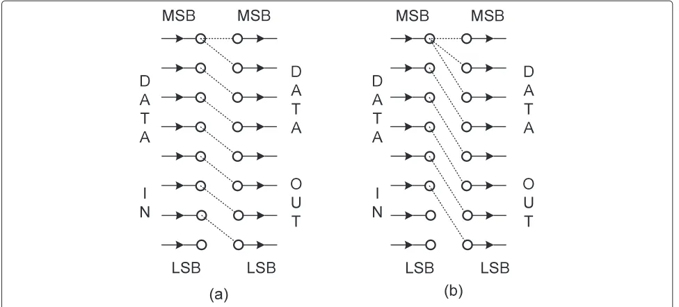
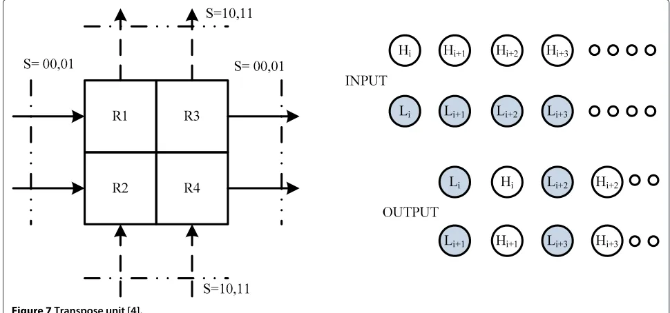
CPU accepts column-wise data, which is managed through efficient TU architecture described in [4]. TU exploits the decimation characteristic of lifting scheme.
TU is composed of four registers and two 4×2
multiplex-ers. Input/output sequences and block diagram of TU are
shown in Figure 7, whereSis select input of multiplexer.
Block (B1) for lifting (9, 7) filter can be extended by using
two instances of the predict and update modules with 4N
memory buffers.
3.4 Dual-input raster scan block (B2)
A novel architecture block (B2) with dual-input raster
scan is proposed for lifting (5, 3) DWT operation as shown
in Figure 8. Block (B2) is composed of one RPU and two
CPUs. Block (B2) takes two inputs at the rising edge of
clk_2−jin raster scan manner and produces four outputs
at every clock cycle. TU is not required because of the two
dedicated 1-D CPUs. RPU of block (B2) works in the same
manner as of block (B1) and produces two 1-D DWT
coef-ficient (L and H). The 1-D coefcoef-ficients are then given to two independent CPU blocks to produce 2-D DWT coef-ficients as shown in Figure 8. CPU constitutes of three
line buffersLB1,LB2, andLB3 of lengthN/2 to process
N×N image. Predict operation of the CPU is managed
by two previous rows of 1-D coefficient stored inLB1 and
LB2 along with one current on-line coefficient as
third-row input from RPU. Past predict values are stored inLB3
to compute update operation. Therefore, line buffers used
for one CPU is 1.5× N, and since block (B2) uses two
instances of CPU, a total of 3×Nline buffers are required.
Block (B2) for jth-level calculation uses two clock
sig-nals, clk_2−j and clk_2−j_pixel_valid. RPU of block (B2)
uses only clk_2−j, while CPU uses both the clock signals.
RPU remains busy in each clock to process two incom-ing pixels/clock; this justifies 100% HUE for RPU. The CPU uses three rows of 1-D coefficient to produce one row of valid 2-D coefficients as shown in Figure 9. But
the RPU of block (B2) produces two rows of 1-D high and
low coefficients, respectively, so the CPU has to wait for
N/2 clock to save required 1-D coefficient in line buffers
Table 3 Mapping of register bank and predict/update module
Flag Operation Predict/update module
in1 in2 in3
0 Predict On-line R4 R2
1 Update R4 R8 R6
LB1 andLB2 to start predict operation. Due to this fact,
output from the CPU of block (B2) is valid forN/2 clock
cycles and remains constant for next N/2 clock cycles
as shown in Figure 10. Gated clock clk_2−j_pixel_valid
is used to save an extra N/2 buffer, otherwise is
required asLB3, when the CPU does not produce valid
coefficients.
3.5 Single-input recursive block (B3)
Single-input recursive block (B3) consists of RPU and
CPU is shown in Figure 11. RPU and CPU use only single processing unit (pre/upd) to compute predict and update alternately. RPU is shown in Figure 12; it consists of a register bank with eight registers and a predict/update module. Data of register bank are right shifted at every clock cycle. The predict/update receives inputs from the register bank and performs predict and update operations alternately, i.e., for two clock cycles predict and for the next two clock cycles update. Mapping of the register bank with inputs of predict/update module is shown in Table 3. Flag input is used to determine predict or update opera-tion. The flag remains ‘0’ for two clock cycles and ‘1’ for next two clock cycles. Input pixel (on-line) is given to
reg-isterR1, and output is taken from registerR4 andR8. The
output of predict/update module is written in registerR3
Figure 14CPU of recursive blockB3for lifting (5, 3) filter.
and R7. Complete data flow of register bank of RPU is
shown Figure 13.
CPU consists of line buffers and a predict/update mod-ule as shown in Figure 14 and works in a similar manner to the RPU. The CPU consists of four line buffers of
sizeNto store 1-D coefficients and intermediate predict
values. Data flow of memory bank is similar to regis-ter bank. 1-D coefficients for first and second rows of input (1st and 2nd) are stored in line buffer LB1 and LB2, respectively. Then, when the first 1-D coefficient for the
Figure 16Folded multi-level architecture (FMA).
third row (3rd) comes, the predict/update module starts operation on third row (on-line) with data of LB1 and LB2 as shown in Figure 15. Predict/update module com-putes predict value and stores it in the first location of LB3, at the same time CPU stores third row of 1-D coef-ficient in LB2, whose current content value in 2nd row is no longer needed. Then onward, when CPU stores 1-D coefficient for third row in LB2, predict value is stored in the LB3, moving from left to right, until all columns are processed. When the 4th row is on-line, predict/update module computes update value from output of LB1, LB3, and LB4, at the same time the 4th row of 1-D coeffi-cient is stored in LB1, whose current content value 1st row is no longer needed. The process continues until all 2-D coefficients are generated for the input image. The proposed memory organization is extremely efficient such that four line buffers are used to store all intermediate 1-D coefficients and predict values. RMA for lifting (9, 7) can be designed using two instances of RPU and CPU in block (B3).
Table 4 Function of control pin in PMA
Control (ctr) Level of decomposition
000 1
001 2
010 3
011 4
100 5
3.6 Multi-level design
3.6.1 Folded multi-level architecture
Block diagram of the proposed folded multi-level archi-tecture is shown in Figure 16. It is composed of
dual-input Z-scan block (B1), multiplexer and memory module
(RAM). The multiplexer either selects input data from the image for the first-level decomposition or from RAM for
higher-level decompositions. Block (B1) takes two inputs
and produces two outputs. Since LL coefficient is
pro-duced alternately, the output of block (B1) is saved in
RAM at half clock rate. Complete data flow is shown in
Table 2. RAM of length N2/4 is used to store jth-level
LL coefficients to obtainjth+1 level of decomposition. In
this scheme, next level decomposition can start only after completion of previous level decomposition, known as level-by-level decomposition. This procedure is repeated until the desired level of decomposition is obtained. FMA for lifting (9, 7) filter is implemented by replicating predict
and update modules in block (B1).
3.6.2 Pipelined multi-level architecture (PMA)
The proposed PMA to perform 5-level lifting (5,3)-based 2-D DWT is shown in Figure 17. The proposed archi-tecture is composed of one instance of dual-input Z-scan
Figure 18Timing diagram of clock, gated clocks, and enable signals for lifting (5, 3)-based PMA.Nis the input image width/height.
block (B1) and four instances of dual-input raster scan
block (B2). Here, the blocks (B1) and (B2) perform
first-level and higher-first-level 2-D DWT decomposition, respec-tively. In the proposed PMA, all 2-D DWT modules oper-ate parallel with dual input. Each single-level processor
computes 2-D DWT independently and outputs the low-frequency (LL) coefficient to the next level. The proposed architecture takes two 8-bit inputs and produces four 16-bit output coefficients. Designed control path is respon-sible to decide the number of decomposition level as per
Table 5 Performance comparison of 2-D DWT architectures
Architecture Mul. Add. Buff. C.P. Thr. C.C. HUE (%)
DSA [10] 12 16 4N 4Tm+8Ta 1 N2/2 100
Wu [3] 6 8 4N Tm 1 N2 100
FA [13] 10 16 5.5N Tm+2Ta 2 N2/2 100
HA [13] 18 32 5.5N Tm+2Ta 4 N2/4 100
Lai [4] 10 16 4N Tm 2 N2/2 100
Zhang [5] 10 16 4N Tm 2 N2/2 −
Hsia [6] 0 16 4N 2Tm+4Ta 2 3N2/4 −
Darji [7] 10 16 4N Tm 2 N2/2 100
Mul., multipliers; Add., adders; Buff., buffers; C.P., critical path; Thr., throughput; C.C., computational cycle; P, parallel factor; HUE, hardware utilization efficiency.
Table 6 Hardware and time complexity comparison of the proposed FMA for lifting (5, 3) filter
Architecture Multipliers/ Adders/ Memory Computing Output Critical HUE (%)
shifters subtractors On-chip Off-chip time forjlevel latency path delay
Andra [8] 4 8 N2+4N 0 2N2(1−4−j)/3 2N 2Ta+2Ts 100
Wu [3] 4 8 5N N2/4 2N2(1−4−j)/3 2N 2Ta+Tm 100
Barua [22] 4 8 5N N2/4 2N2(1−4−j)/3 5N Tm 100
Xiong [13] FA 4 8 3.5N N2/4 2N2(1−4−j)/3 N 2Ta+Tm 100
Xiong [13] HA 8 16 3.5N N2/4 N2(1−4−j)/3 N 2Ta+Tm 100
FMA 4 8 2N N2/4 2N2(1−4−j)/3 N Ta+Ts 100
Input image sizeN×Nandj≥1. Ta, adder delay; Tm, multiplier delay; Ts, shifter delay.
Table 7 Comparison of hardware and time complexity of the proposed FMA for lifting (9, 7) filter
Architecture Multipliers/ Adders/ Memory Output Computing Critical HUE (%)
shifters subtractors On-chip Off-chip latency time forjlevel path delay
Andra [8] 32 32 N2 0 N2/2 4N2(1−4−j)/3 4Ta+2Tm 100
Wu [3] 6 8 5.5N N2/4 ∼ 2N2(1−4−j)/3 Tm 100
Barua [22] 12 16 7N N2/4 7N 2N2(1−4−j)/3 2Ta+Tm 100
Xiong [13] FA 10 16 5.5N N2/4 2N 2N2(1−4−j)/3 2Ta+Tm 100
Xiong [13] HA 18 32 5.5N N2/4 N N2(1−4−j)/3 2Ta+Tm 100
FMA 10 16 4N N2/4 N 2N2(1−4−j)/3 Ta+Tm 100
Input image sizeN×Nandj≥1. Ta, adder delay; Tm, multiplier delay; Ts, shifter delay;∼, not available.
Table 8 Comparison of hardware and time complexity of the proposed PMA for lifting (5, 3) filter
Architecture Multipliers/ Adders/ Memoryj=1 Computing Latency Critical HUE (%) shifters subtractors On-chip Off-chip cycle forjlevel j=1 path delay
Hasan [23] 2j j 3N 0 O(N2) 3N 2Ta+Ts 100
Aziz [15] 2j 4j 4N 0
j m=1
1+23mN−1+ N 2
22(m−1) 3N+1 2Ta 50 to 60
PMA 4+6(j−1) 8+12(j−1) 2N 0 2+ j m=1
10+2mN−1+ N 2
22m−1 N+12 Ta+Ts 60 to 75
Table 9 Line buffer comparison for PMA for lifting (5, 3) filter
Architecture Memory
Forj=1 Forj=5
Aziz [15] 4N 4N+2N+N+N
2 +N4 ≈7.7N
PMA 2N 2N+3N
2 +34N+38N+316N≈4.8N Input image sizeN×N.
the need of application as described in Table 4. Due to decimation property of wavelet transform, at each level,
total computation is reduced to 1/4 than the preceding
stage. To maintain a dual-input processing at every level
of decomposition, the clock rate is set as 1/2 than the
preceding stage through a timing control circuit. Serial input and parallel output (SIPO) is used in between 2-D 2-DWT modules for pipelining as shown in Figure 17. SIPO block is composed of two registers, which are filled with serial input coming from the previous pipelined stage at the rising edge of clock (clk2−(j−1)) and output
is taken at half clock rate (clk2−j) as shown in Figure 17.
PMA for lifting (9, 7) filter can be implemented by
repli-cating predict and update modules twice in blocks (B1)
and (B2).
Clock gating is a well-known method to reduce dynamic power dissipation in synchronous digital circuits by adding more logic to a circuit to prune the clock tree (clock distribution network). Pruning the clock disables portions of the circuitry and thus saves the power. Clock gating also saves significant die area, as it removes a large number of multiplexers and replaces them with clock gating logic. Mainly, five clock signals are gener-ated clk2−1, clk2−2, clk2−3, clk2−4, clk2−5fromclk. Clock clk2−jis 1/2−jrate of clk, wherejindicates decomposition
level. Period of enable signal isN/2 and signals enable1,
enable2, and enable3 are generated from it with period
N, 2N, 4N, respectively. clk_2−2 is generated by logical
AND operation of clk2−2 and enable signal. clk_2−3 is
generated by logical AND operation of clk2−3, enable,
and enable1, and in the same way, clk_2−4 and clk_2−5
are generated. clk_2−2_pixel_valid is generated from
log-ical AND of clk2−2, enable, and enable1; in the same
way, clk_2−3_pixel_valid is generated from clk2−3, enable,
enable1, and enable2 as shown in Figure 18. Clocks and
enable used by second-level and third-level block (B2) are
shown in Figure 17. Every block (B2) operates on two
gated clocks signals, clk_2jand clk_2j_pixel_valid.
3.6.3 Recursive multi-level architecture
The proposed RMA is composed of blocks (B1) and (B3)
as shown in Figure 19. Block (B1) is employed to process
the input image to get first-level 2-D DWT coefficients,
and block (B3) works recursively for computing
multi-level coefficients. RMA requires line buffer for temporary
storage of coefficients generated from the block (B3). A
multiplexer is used at the input of block (B3) to select the
input sample either from block (B1) or from line buffers.
Careful management of the switching of this multiplexer
utilizes the idle interleaved clock cycles of block (B3)
to process higher-level coefficients such that maximum hardware utilization is achieved.
Block (B1) produces LL coefficient at alternate clock
cycle, which is fed to block (B3) for multi-level processing.
Block (B3) is designed such that it operates one
sam-ple per clock cycle. The block (B3) also has a feedback
mechanism that brings the higher-level LL coefficients at the input to compute next higher-level coefficients. A
buffer of size less than N/2 is used to store
intermedi-ate LL coefficients. This buffer is divided into different
lengths, such as N/4,N/8,N/16. . .to store one row of
LL coefficients. These buffered LL coefficients are
seri-ally provided to block (B3) to get next higher-level DWT
coefficients. Here, a multiplexer is used, which is operated on the control signal ctr_2 and provides first- and higher-level LL coefficients at alternate clock cycle. Thus, every clock cycle is utilized to process the first- and higher-level LL coefficients alternatively. Valid multi-level coefficients are available at every fourth clock cycle. The depth of
Table 10 Comparison of hardware and time complexity of the proposed PMA for lifting (9, 7) filter
Architecture Mohanty [14] Mohanty [21] Hu [19] Proposed PMA
Scheme LT CV LT LT
Multiplier 6Px3 189 1058S+6 32
Adder 32Px3/3 294 21S+12 64
Registers N(11x2+10x5) 214N+443 3N+3418S 48
Line buffers 0 0 0 4N+24N
ACT NP2 N162 N2S2 N22+2N2
Critical path delay 2Ta+Tm ≈Tm Ta+Tm Ta+Tm
Input image sizeN×Nandj= 3. L.B., line buffer; P, number of samples processed per clock cycle; S, strip size; Ta, adder delay; Tm, multiplier delay;
Table 11 Hardware and time complexity of the proposed RMA
Architecture Mult./ Add./ Memoryj=1 Output Critical HUE (%)
shift. sub. On-chip Off-chip latency path delay
RMA (5, 3) 6 12 6.5N 0 2N 2Ta+Tm 75
RMA (9, 7) 16 24 12.5N 0 4N 2Ta+Tm 75
Input image sizeN×Nandj≥1. Ta, adder delay; Tm, multiplier delay; Ts, shifter delay.
the data is decreased fourfold at each level of operation,
i.e., first-level data depth is decreased fromN2to N2/4,
second level toN2/16, and so on. This property of
inher-ent compression is utilized for pushing the higher-level coefficients into buffers.
4 Performance analysis and comparison
In this section, architecture performance is evaluated based on following parameters: HUE, speed, computing time, output latency, line buffers, complexity of control circuit, number of adders and multipliers, system power consumption, configurable logic block (CLB) slices, crit-ical path delay, memory, and maximum frequency of operation. The % HUE is defined by (5).
%HUE= Number of block in use
Total number of blocks ×100 (5)
Pipelining is done between predict and update stages in FMA, PMA, and RMA to reduce the critical path delay
from conventional 4Ta+ 2Tmto only Ta+Tsfor
lift-ing (5, 3) andTmfor lifting (9, 7) at the cost of latency
of few clock cycles. Total 2N on-chip line buffers are
required in the proposed FMA and PMA for lifting (5, 3)
andj = 1 level, which is lowest among existing
archi-tectures. The latency of the proposed scheme isNcycles
(without boundary treatment). The proposed RMA uti-lizes only one processing element to calculate both predict and update, resulting into 50% reduction in number of adders and multipliers.
4.1 Hardware complexity and timing analysis
Hardware complexity is mainly sensitive to number of adders, multipliers, on-chip buffers, and control path. Per-formance comparison of 2-D DWT architecture is given in Table 5. Hardware complexity of folded multi-level
structure is reported in literature as [3,8,10,13,22] is
com-pared in Table 6 and Table 7, respectively, for thej-level
of decomposition. HA structure in [13] appears to be the best in terms of computing cycles, but it requires 8 multipliers and 16 adders. The proposed FMA has only half-area requirement in terms of on-chip mem-ory buffers, adders/subtractors, and multiplier/shifter required as compared to HA. Moreover, the critical path
delay of the proposed FMA for lifting (5, 3) isTa+Ts,
which is lowest among similar architectures. Structure in Wu and Lin [3] appears to be the best for lifting (9, 7) in terms adder, multiplier and critical path delay but requires
5.5N on-chip buffers for processing as compared to the
proposed FMA. The critical path delay of the proposed
FMA for (9, 7) isTa+Tm, and it requires only 4Non-chip
buffers. Hardware and time complexity of the proposed PMA for lifting (5, 3) filter are compared in Table 8 with the architectures described in literature with similar spec-ifications, such as [15] and [23]. The proposed PMA has not only the lowest critical path but it also requires less computing cycles as shown in Table 8. The extra two cycles in the total computing cycle are added due to
trans-position in block (B1). It must be also observed that the
architecture proposed by Hasan et al. [23] utilizes less number of multipliers and adders but requires more line buffers to compute multi-level 2-D DWT. It is evident
from Table 9 that the PMA uses 4.8N line buffers, while
the architecture given [15] required 7.7Nline buffers for
five-level DWT decomposition using lifting (5,3) filter.
N2
2 +10
+
N
2 +8
+
N
4 +8
+
N
8 +8
+
N
16+8
=N2
2 +
15N
16 +42
(6)
Table 12 Comparison of hardware and time complexity of the proposed RMA for (9, 7) with existing architectures
Arch. Mult. Add. Line buffers Control complexity Computing time
Liao [10] 12 16 10N(1−2−j) Medium N2/2
Xiong [16] 28 48 10N(1−2−j)+0.5N Medium N2/4
RMA 16 24 12.5N Simple N2/2
Table 13 FPGA synthesis results for FMA: image size 256×256
Architecture FMA (5, 3) FMA (9, 7)
FPGA Virtex-5 Virtex-5
Device 5VLX110TFF1136-3 5VLX110TFF1136-3
Slice LUTs 494(0%) 1008(1%)
Slice registers 633(0%) 1091(1%)
MUF (MHz) 537 210
MUF, maximum utilization frequency.
A total computing cycle required by PMA for five-level
decomposition of an image (sizeN×N) is shown in (6).
All single-level processors (B1 andB2) work in a
paral-lel fashion in PMA. Block (B1) utilizes N22 +10 , and
remaining clocks are consumed in consecutive four blocks
of (B2). So, most of the processing is done withinN2/2
clock cycles and very small additional cycles, i.e., (N/2+8), (N/4+8), (N/8+8), and (N/16+8) are needed to compute further levels.
Architecture comparison of the proposed PMA with [14,19,21] for three-level 2-D DWT using lifting (9, 7) filter is shown in Table 10. The proposed architecture uses lowest number of multipliers and adders as com-pared to other architectures. Architectures [14,19,21] do not use any line buffers at the cost of more computation logic and complex control path.
The hardware complexity of the proposed RMA for lift-ing (5, 3) and (9, 7) is shown in Table 11. The RMA for lifting (5, 3) uses a total of six multipliers, out of which four
are used in block (B1) and two are used in block (B3). In
case of RMA for lifting (9, 7) filter, a total of 16 multipliers
are required, out of which 10 are utilized in block (B1) and
6 are used in block (B3). The additional two multipliers
are required to scale output coefficients. Block (B1) uses a
total 2Nand 4Nline buffers for lifting (5, 3) and lifting (9, 7) filters, respectively. The number of buffers and multi-pliers required for (9, 7) filter is double than that for (5, 3).
HUE of block (B1) is 100%, but block (B2) has some
inter-leaved clock cycles that results into 75% HUE of all over RMA.
Hardware and time complexity of the proposed RMA for lifting (9, 7) are compared with architectures proposed by [10] and [16] in Table 12. The proposed RMA uses a
total of 16 multipliers, out of which block (B1) uses 10 and
block (B3) uses 6. Numbers of adder utilized by blocks
(B1) and (B3) are 16 and 8, respectively. 4N line buffers
are used by block (B1), 8N are consumed by block (B3),
and 0.5N are used in storing intermediate-level
coeffi-cient, which resulted in a total of 12.5Nline buffers in the
design of RMA. The proposed RMA is simple and reuses same processing element to compute predict and update values. The proposed architecture requires less multipli-ers, addmultipli-ers, and computing time as compared to [16]. Liao et al. [10] require the lowest number of multipliers and adders because it uses only one 2-D DWT block, but require more complex control path as compared to the proposed RMA.
4.2 FPGA Implementation
The proposed FMA for lifting (5, 3) and (9, 7) filters is implemented on Xilinx Virtex-5 XC5VLX110T FPGA tar-get device (Xilinx, Inc., San Jose, CA, USA), and the results are reported in Table 13. The maximum utilization fre-quency (MUF) for FMA is very high as a result of very low
critical path delay, i.e.,Ta+TsandTa+Tmfor lifting (5,
3) and (9, 7) filters, respectively.
The proposed PMA for five-level lifting (5, 3) is synthesized using Xilinx ISE 10.1 for Xilinx Virtex-5 XC5VLX110T FPGA target device, and the results are reported in Table 14. Sixteen-bit word length is used in the proposed scheme for higher-level decomposition without overflow. Since the pipelined processor element is used in the design, 537-MHz frequency of operation is obtained. The CLB count reported in [15] is less than that in the pro-posed scheme because of folded processor element, but this approach leads to lower throughput. Throughput is calculated by (7). The proposed PMA utilizes 1,178 slices and provides throughput rate of 4,080 frames/s for
lift-ing (5, 3) for 512×512 frame resolution. This is almost
five times more than [15]. Power is estimated using Xil-inx X-power at a 100-MHz frequency and reported in Table 14. It is apparent from this comparison that the proposed scheme consumes lower power as compared
Table 14 FPGA synthesis results of the proposed PMA for lifting (5, 3) 2-D DWT
Architecture Power forj=1 (mW) Frequency CLB slice count Throughput frames/s
Dynamic Quiescent Total Forj=1 Forj=5
Aziz [15] 33.85 1,186.94 1,220.79 221.44 206 1,052 835
PMA without clk gating 29.6 980.8 1,010.6 539 412 1,329 4,080
PMA with clk gating 28 980.8 1,008.2 539 342 1,178 4,080
Table 15 Comparison of FPGA synthesis results for RMA: image size 256×256 andj=3
Arch. Liao [10] Xiong [16] RMA (5, 3) RMA (9, 7)
FPGA Virtex-4 Virtex-4 Virtex-4 Virtex-4
Device 4VFX100FF1152-12 4VFX100FF1152-12 4VFX100FF1152-12 4VFX100FF1152-12
LE/slices 1,180 2,532 1,040 1,822
LE, logic elements or cells.
to [15] because of dual-scan technique and lower line buffers are used in design implementation.
Throughput=Fmax/Total clocks required for a frame transform
(7)
The proposed RMA is synthesized for lifting (5, 3) and (9, 7) filters using Xilinx ISE 10.1 for Xilinx Virtex-4 XCVirtex-4VFX100 FPGA target device, and the results are reported in Table 15. The RMA implementation uses 1,822 (4%) and 1,040 (2%) slices for lifting (9, 7) and (5, 3) filters, respectively. The output of FMA using lifting (9, 7)
filter withj = 1 and RMA using lifting (9, 7) filter with
j = 3 is shown in Figure 20. Output of PMA for lifting
(5, 3) filter withj = 1 to j = 5 levels for input image
Cameraman (256×256) is shown in Figure 21.
5 Conclusions
In this paper, we have proposed high-performance FMA, PMA and RMA with dual-pixel scanning method for computing multi-level 2-D DWT. The architectures are compared on the basis of resources utilized and speed. Micro-pipelining is employed in predict/update
proces-sor element to reduce the critical path to Ta+Ts and
Ta+ Tmfor lifting (5, 3) and (9, 7) filters, respectively.
Optimized single-level 2-D DWT blocks (B1), (B2), and
(B3) are proposed to design multi-level architecture. The
proposed FMA for lifting (5, 3) and lifting (9, 7) uses only
2Nand 4Nline buffers, respectively. The proposed PMA
is simple, regular, modular, and can be cascaded forn-level
decomposition. The PMA for lifting (5, 3) has a critical
path delay of Ta+Ts. Moreover, it requires only 4.8N
line buffers for five-level decomposition, thus reduces line buffer approximately 50% than other similar designs. The proposed RMA uses 16 multipliers and 24 adders for
n-level decomposition. Moreover, a requirement of line
buffers is independent of level of decomposition. The proposed architectures are implemented on Xilinx Virtex family devices. The proposed FMA and PMA operate with frequency of 537 MHz, which is sufficient to handle 518
full-HD frames with 1, 920×1, 080 resolution. The
pro-posed PMA, when implemented on FPGA for five-level DWT, utilizes 1,178 slices and provides a throughput rate
of 4,080 frames (512×512) per second, which is almost
five times than that of the existing design. The proposed RMA uses unique buffer management and only single pro-cessing element for computing predict and update to save area and power. The Xilinx Virtex-4 implementation of RMA uses 1,822 (4%) and 1,040 (2%) slices for lifting (9, 7) and (5, 3) filters, respectively.
FPGA implementation of the proposed schemes show higher operating frequency, low latency, and lower power as compared to other architectures with the same specifications. The proposed designs can be used for
Figure 21PMA output.(a)Original image.(b)One-level,(c)two-level,(d)three-level,(e)four-level, and(f)five-level lifting (5, 3) 2-D DWT decomposition of image size 256×256.
practical applications with power, area, and speed con-strains. The proposed architectures are suitable for high-speed real-time systems such as image de-noising, on-line video streaming, watermarking, compression, and multi-resolution analysis.
Competing interests
The authors declare that they have no competing interests.
Author details
1Department of Electrical Engineering, Indian Institute of Technology Bombay, Powai, Mumbai 400076, India.2Electronics Engineering Department, S. V. National Institute of Technology, Surat, Gujarat 395007, India.
Received: 26 January 2014 Accepted: 29 September 2014 Published: 4 October 2014
References
1. I Daubecies, W Sweldens, Factoring wavelet transforms into lifting steps. J. Fourier Anal. Appl.4, 247–269 (1998)
2. J-M Jou, Y-H Shiau, C-C Liu, Efficient VLSI architectures for the
bi-orthogonal wavelet transform by filter bank and lifting scheme, inProc. IEEE International Symposium on Circuits Systems (ISCAS), vol. 2 (Sydney, New South Wales, 06–09 May 2001), pp. 529–532
3. B Wu, C Lin, A high-performance and memory-efficient pipeline architecture for the 5/3 and 9/7 discrete wavelet transform of JPEG2000 codec. IEEE Trans. Circuits Syst. Video Technol.15(12), 1615–1628 (2005)
4. Y-K Lai, L-F Chen, Y-C Shih, A high-performance and memory-efficient VLSI architecture with parallel scanning method for 2-D lifting-based discrete wavelet transform. IEEE Trans. Consum. Electron.55(2), 400–407 (2009) 5. W Zhang, Z Jiang, Z Gao, Y Liu, An efficient VLSI architecture for
lifting-based discrete wavelet transform. IEEE Trans. Circuits Syst. II.59(3), 158–162 (2012)
6. C-H Hsia, J-S Chiang, J-M Guo, Memory-efficient hardware architecture of 2-D dual-mode lifting-based discrete wavelet transform. IEEE Trans. Circuits Syst. Video Technol.25(4), 671–683 (2013)
7. A Darji, S Agrawal, A Oza, V Sinha, A Verma, SN Merchant, A Chandorkar, Dual-scan parallel flipping architecture for a lifting-based 2-D discrete wavelet transform. IEEE Trans. Circuits Syst. II, Exp. Briefs.61(6), 433–437 (2014)
8. K Andra, C Chakrabarti, T Acharya, A VLSI architecture for lifting-based forward and inverse wavelet transform. IEEE Trans. Signal Process.50(4), 966–977 (2002)
9. C-T Huang, P-C Tseng, L-G Chen, Efficient VLSI architectures of lifting-based discrete wavelet transform by systematic design method, in Proceedings of the IEEE International Symposium on Circuits and Systems, vol. 5 (Scottsdale, Arizona, 26–29 May 2002), pp. 565–568
10. H Liao, MK Mandal, BF Cockburn, Efficient architectures for 1-D and 2-D lifting-based wavelet transforms. IEEE Trans. Signal Process.52(5), 1315–1326 (2004)
11. P-Y Chen, VLSI implementation for one-dimensional multilevel lifting-based wavelet transform. IEEE Trans. Comput.53(4), 386–398 (2004) 12. BK Mohanty, PK Meher, VLSI architecture for high-speed / low-power
implementation of multilevel lifting, DWT, inProceedings of the IEEE Asia Pacific Conference on Circuits and Systems(Singapore, 4–7 Dec 2006), pp. 458–461
13. C Xiong, J Tian, J Liu, Efficient architectures for two-dimensional discrete wavelet transform using lifting scheme. IEEE Trans. Image Process.16(3), 607–614 (2007)
14. BK Mohanty, PK Meher, Memory efficient modular VLSI architecture for highthroughput and low-latency implementation of multilevel lifting 2-D DWT. IEEE Trans. Signal Process.59(5), 2072–2084 (2011)
15. SM Aziz, DM Pham, Efficient parallel architecture for multi-level forward discrete wavelet transform processors. J. Comp. Elect. Eng.38, 1325–1335 (2012)
16. C-Y Xiong, J-W Tian, J Liu, Efficient high-speed/low-power line-based architecture for two-dimensional discrete wavelet transform using lifting scheme. IEEE Trans. Circuits Syst. Video Technol.
16(2), 309–316 (2006)
17. C-H Hsia, J-M Guo, J-S Chiang, Improved low-complexity algorithm for 2-D integer lifting-based discrete wavelet transform using symmetric mask-based scheme. IEEE Trans. Circuits Syst. Video Technol.19(8), 1202–1208 (2009)
18. AK Al-Sulaifanie, A Ahmadi, M Zwolinski, Very large scale integration architecture for integer wavelet transform. J. IET Comp. Digital Tech.
19. Y Hu, CC Jong, A memory-efficient high-throughput architecture for lifting-based multi-level 2-D DWT. IEEE Trans. Signal Process.61(20), 4975–4987 (2013)
20. ME Angelopoulou, K Masselos, PY Cheung, Y Andreopoulos, Implementation and comparison of the 5/3 lifting 2-D discrete wavelet transform computation schedules on FPGAs. J. Signal Process. Syst.51(1), 3–21 (2008)
21. BK Mohanty, PK Meher, Memory-efficient high-speed convolution-based generic structure for multilevel 2-D DWT. IEEE Trans. Circuits Syst. Video Technol.23(2), 353–363 (2013)
22. S Barua, JE Carletta, KA Kotteri, AE Bell, An efficient architecture for lifting-based two-dimensional discrete wavelet transforms. J. Integration, VLSI J.38(3), 341–352 (2005)
23. H Varshney, M Hasan, S Jain, Energy efficient novel architectures for the lifting-based discrete wavelet transform. IET Image Process.1(3), 305–310 (2007)
doi:10.1186/1687-5281-2014-47
Cite this article as:Darjiet al.:High-performance hardware architectures for multi-level lifting-based discrete wavelet transform.EURASIP Journal on Image and Video Processing20142014:47.
Submit your manuscript to a
journal and benefi t from:
7Convenient online submission
7 Rigorous peer review
7Immediate publication on acceptance
7 Open access: articles freely available online
7High visibility within the fi eld
7 Retaining the copyright to your article