Copyright © 2015 CTTS.IN, All right reserved
Designing and Improvement of a New Reversible Floating
Point Adder
Fatemeh Alaghemand
MSc. Student, Department of Computer Engineering, Dezful Branch, Islamic Azad University, Dezful, [email protected]
Majid Haghparast
Assistant Professor, Department of Computer Engineering, Yadegar -e- Imam Khomeini (RAH) Branch, Islamic Azad University, Tehran, [email protected]
Abstract – In recent years, reversible logic has been proposed as an emerging technology that can be used in quantum computing, optical computing and nanotechnology. A necessary condition for the reversibility of a computational model is that there should be a unique one-to-one mapping between the inputs and outputs. Conventional gates, however, do not have this capability; thus, reversible gates are designed, and reversible circuits are manufactured by the gates. Measures of quantum cost, the number of constant inputs and the number of garbage outputs are calculated to evaluate the performance of these circuits. In this study, we have decided to design a reversible floating point adder, capable of summing the floating point numbers and minimizing the quantum cost, the number of garbage output and the number of constant input opposed to prior designs.
Keywords – Floating point adder, Nanotechnology, Quantum cost, Reversible logic.
1. I
NTRODUCTIONAccording to Moore's law, every 18 months up to two years, the number of transistors on a chip with the same size will double. Researchers have concluded that in coming years, because of the transistors' heat, Moore's Law will show some limitations. If transistors placed in a closer distance on the chip, will dissipate more heat and lose internal energy [1].
In 1961, Landauer proved that processing in non-reversible circuits (conventional circuit) causes loss of energy, and the energy dissipation per bit of data during the computation is KTLn2 Jules, where K=1.3806505×10⁻²³(Joules/Kelvin)is Boltzmann's constant and T is the absolute temperature of the environment at which the process occurs [2].In 1973, Bennett showed, if a circuit is made of reversible gates, the heat dissipation will be zero, because reversible circuits avoid bit loss trough unique mapping between the input and output vectors and reusing the information instead of discarding it[3].
Given the fact that one important goal in hardware design is the design of circuits with low power consumption, the use of reversible gates in circuits in the coming years will become an imperative. In other words, reversible circuits, in the near future will replace the current conventional circuits.
Adding is one of the most widely used mathematical operations, and so far several reversible adders have been designed for fixed point numbers. However, floating-point operations have more precision. In present study, we intended to design a reversible floating point adder circuit.
This paper is divided into six parts. Section 2 reviews basic definitions and reversible gates, Section 3 outlines a floating-point addition algorithm and architecture and describes briefly the existing designs, and Section 4 shows our proposed designs. The comparison between the existing designs and our proposed design and the conclusion are in Parts 5 and 6 respectively.
2. B
ASICD
EFINITIONSA
NDR
EVERSIBLEG
ATESR
EVIEWReversible logic and measuring parameters for reversible gates are introduced in the following section:
2.1. Definitions
Reversible logic: A function f, is reversible if and only if there exists a function g such that x = g (f (x)) for all xs in the domain of f. In other words, f is called reversible if: a. The number of outputs is equal to the number of inputs;
b. Any output vector has a unique mapping input vector [4].
Reversible gate: Gates which have an equal number of input and output are defined as reversible gates. Reversible gates have a one-to-one correspondence between the input and output vectors. That is, we can determine the outputs from the inputs and also uniquely recover the inputs from the outputs [5].
An N*N reversible gate can be represented as:
Iv= (I1,I2,I3,I4,……….…IN)
Ov= (O1,O2,O3,……….ON).
Where Iv represents the input vector and Ov is the output
vector.
Minimizations of the number of quantum cost, garbage outputs, and constant inputs have an important role in the design of a reversible circuit.
Copyright © 2015 CTTS.IN, All right reserved Quantum cost (QC): The quantum cost of a reversible
gate is the number of 2×2 reversible gates required in designing it. The quantum cost of all reversible 2×2 gates is taken as 1 and the cost of allthe1×1 reversible gates is assumed to be zero [8].
Constant inputs (CI): The inputs that are added to an n×k gate to make it k × k gate are called constant inputs [8]. These inputs are to be kept constant at either 0 or 1 in order to synthesize the given logical function [7].
2.2.Reversible Gates Review
A set of reversible logic gates is needed to synthesize reversible circuits. Several reversible gates have been proposed in the literature, such as Feynman [9], Toffoli [10], Fredkin [12], TR [13], etc. The most important of which are as follows:
NOT gate: The only 1×1 reversible gate is an inverter. This gate is very important because it produces no garbage outputs and has zero quantum cost [5]. The Not Gate is shown in Fig. 1a.
Feynman gate (FG): One of the most consequential reversible logic gates is the Feynman Gate, also called Controlled NOT gate (CNOT). This gate is a 2×2 reversible logic gate and can be represented as:
Iv = (A, B)
Ov = (P = A, Q = A⊕B)
Where Iv represents the input vector and Ov is output
vector. A 2×2 Feynman gate is shown in Fig.1b, 1c. Its quantum cost is 1[9].
Fig1. NOT gate (a), Feynman gate (b, c)
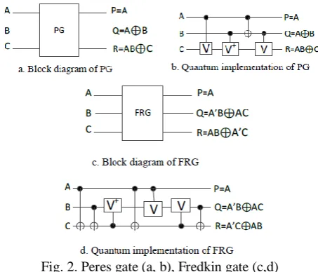
Peres gate (PG): Peres gate is a 3×3 reversible gate. It can be shown as:
Iv = (A, B, C)
Ov = (P = A, Q = A⊕B, R = AB⊕C)
Where Iv represents the input vector and Ov is output
vector.
Fig.2a, 2b shows the Peres gate. Its quantum cost is 4. In the existing literature, among 3×3 reversible gates, Peres gate has the minimum quantum cost [11].
Fredkin Gate (FRG): Fredkin gate is shown in Fig. 2c, 2d and can be described as:
Iv = (A, B, C)
Ov = (P = A, Q = A'B⊕AC, R = AB⊕A'C)
Where Iv represents the input vector and Ov is output
vector.
It is also known as swap gate. If the control input is A=’0’ then inputs B and C are shown clearly in outputs, else if A= ’1’ then inputs B and C are swapped and shown in outputs, FRG has a quantum cost of 5 [12].
Fig. 2. Peres gate (a, b), Fredkin gate (c,d)
MUX gate: MUX gate is a 3×3 reversible gate shown in Fig. 3a. Its functionality is represented as:
Iv = (A, B, C)
Ov = (P = A, Q = A⊕B⊕C, R = AB⊕A'C)
Where Iv represents the input vector and Ov is output
vector.
This gate can work as a reversible 2:1 Multiplexer. When input A is ‘0’ data on input line C is chosen and put on the output line R. When input A is ‘1’ data on input line B is chosen and put on the output line R. Therefore, input line A acts as a control line and input lines C and B act as data input lines. The quantum cost of this gate is 4 [14].
HNG gate: A 4* 4 reversible HNG gate can be described as:
Iv = (A, B, C, D)
Ov = (P = A, Q = B, R = A⊕B⊕C, S=
(A⊕B).C⊕AB⊕D)
Where Iv represents the input vector and Ov is output
vector.
Copyright © 2015 CTTS.IN, All right reserved Fig. 3. MUX gate (a), HNG gate (b, c)
3. A
LGORITHMA
NDE
XISTINGD
ESIGNImplementation of floating point operations depends on the particular format applied to display the operands.
Conditional Swap
Alignment
Sign-magnitude to 2's complement Sign-magnitude to 2's complement
Addition
2's complement to sing-magnitude
Normalization and Rounding
A+B
e
xp
on
en
t d
iff
er
en
ce
B A
X Y
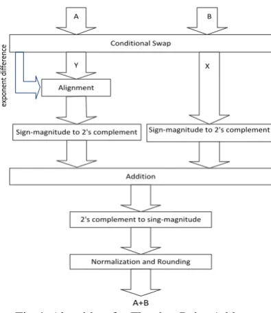
Fig.4. Algorithm for Floating Point Adder
Two 32-bit (1 sign bit, 8-bit exponent, 23-bit mantissa) floating point numbers A and B in IEEE-754 standard are to be added. In the standard form, the exponents of both operands must be equal before adding the mantissa. To satisfy this condition, the smaller number's exponent should be incremented until it reaches the larger number's, and them antissa be aligned by shifting the mantissa of the smaller operand to the right, its exponent is incremented at the same time, until it equals the other exponent. When the exponents are equal, the mantissa can be summed. Finally, the sum is normalized and
rounded. Fig.4 shows the general algorithm of the floating point architecture. Since two reversible floating point addersin [16], [17] are designed, in this section, we present these designs.
3.1. Reversible Conditional Swapping
To identify the number with the smaller exponent and the difference between the two exponents, a reversible conditional swap is necessary. Fig. 5 shows the details of the existing designs. If expA<expB then the two numbers will be swapped; otherwise, nothing should be done. Next, the number with the smaller exponent always comes out in the Y output and goes to the alignment unit.
a. Conditional Swap in [16]
b. Conditional Swap in [17] Fig. 5. Existing Conditional Swaps
3.2. Reversible Alignment
Alignment is necessary because we can only add two mantissas when the two exponents are equal. Therefore, in order to do that, a reversible shifter is needed. The difference between the two exponents is the shifted amount. After the mantissa is shifted, the bits that are shifted out should not be all thrown away since they can possibly affect the rounding of the result. Keeping all the shifted bits will double the width of the mantissa. Therefore, the three bits, namely, G (guard), R (round) and S(sticky) must be used.
Copyright © 2015 CTTS.IN, All right reserved a. Alignment Unit in [16]
b. Alignment Unit in [17] Fig. 6. Existing Alignment units
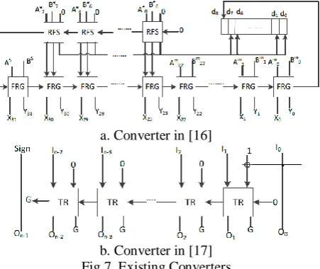
3.3. Reversible Converter
In IEEE-754 standard, numbers are in sign-magnitude format, namely 1 bit for sign and 23-bit for mantissa. After shifting the mantissa of two numbers and before adding them, they must be converted from sign-magnitude representation to two's complement. After the addition, the result will be converted from two's complement to sign-magnitude format. Thus, two 28-bit sign-magnitudes to two's complement reversible converters and one 29-bit two's complement to sign-magnitude reversible converter are needed. The existing designs for converter are shown in Fig.7.
a. Converter in [16]
b. Converter in [17] Fig.7. Existing Converters
3.4. Reversible Addition
For the 28-bit full adder unit, a reversible ripple carry adder consisting of a single reversible half adder (RHA) in the least significant sum position followed by 27 reversible full adders (RFAs) is used. For the RHA, the Peres gate is used, and for the RFA the HNG gate is used. These gates implement the required functionality with the smallest known quantum cost [18], [19].
3.5. Reversible Normalization and Rounding
A floating point number is normalized if the most significant bit of the mantissa is non-zero. In normalization unit, if a shift is needed, it is either one place right shift or several places left shift. If normalization requires a right-shift, only one place must be shifted to the right, and the exponent will need to be added with one. If normalization requires shifting the sum to the left, then the first the number of leading zeros must be counted to be used as a shift amount. Then according to [16] a Reversible Leading Zero Counter (RLZC) is needed. After determining the amount of the left shift, the exponent must be reduced according to the number of zeros. The algorithm of normalization unit is shown in Fig. 8.
Fig.8. Normalization Unit
4. P
ROPOSEDD
ESIGNSince the aim of this study is designing a reversible floating point adder with the least amount of quantum cost, garbage outputs and constant inputs, in this section, we propose a new design according to the algorithm shown in Fig.4.
4.1. Conditional Swap
To add two floating point numbers, the exponents must be equal, so we need a conditional swap circuit. In [16] 9 HNG gates for the construction of reversible full subtractor (RFS) are used while in [17] there are 7 new RFS and 1 new reversible half subtractor (RHS), which are made by the gate TR .
With regard to [17] where the new RHS and new RFS are used, yielding the lowest quantum cost, we also used this design for conditional swap circuit (Fig. 5).
4.2. Alignment Unit
Copyright © 2015 CTTS.IN, All right reserved shows the circuit for 8 bits. This unit has a right barrel
shifter and GRS-bit generation component.
In the (m,k) reversible Alignment, m is the number of mantissa bits, k represents the shift value and the number of exponent bits retained in E. Thus, this circuit will have K+1 rows.
For (8, 3) reversible Alignment, if M=8 and E=5 then d4,d3,d2,d1,d0 lines will be equal to the exponent
difference of the two mantissas where d2,d1,d0 determine
the shift amount, and d4,d3 are used as two inputs of PG
that work as a NOR gate to create the final result and the required GRS-bits. In this design, FRG works as a multiplexer, FG works as fan-out gates and PG works as AND/OR/NOR gates.
Fig.9. Alignment Unit in [20]
4.3. Converter
To add two sign magnitude numbers, first they must be converted to 2's complement, so if the sign bit of the number is one, invert it and add it with 1. We used the MUX gate to design converter in Fig.10. In this design, if sign = 1,first, the least significant bit (LSB) goes to the output unchanged while the other bits are reversed by the FG and go into the MUX gates then added with 1.These MUX gates except the first one works as RHA; otherwise, if sign=0, the bits without change go to the output.
Table.1 compares the two existing designs and our proposed design for converter in quantum cost, garbage output and constant input. The design in [17] because of ignoring the sign bit has less quantum cost.
MUX MUX MUX MUX
On-2 G G G
I1 In-3 In-2 I0 0 0 Sign G On-3
On-1 O1
O0=I0 G
…. …. 0 0
Fig.10. Proposed Converter
Table(1). Comparison between proposed and Existing Converters for 8 bit inputs
Converter for 8 bits QC GO CI
Existing design in [16] 41 9 9 Existing design in [17] 30 9 9
Proposed design 40 9 9
4.4. Normalization and Rounding Unit
Since the designs in [16], [17] both used the algorithm in Fig. 8 to normalize the final result, we applied the same algorithm for the normalization phase, except that the components will change in this case
The complete reversible normalization unit works as follows: If the 28-bit mantissa has a value of one in its MSB, it must be right shifted one place. Therefore, the MSB of the mantissa is connected to the carry input of a RHA to be added with the 8-bit exponent, where the RHAs are made by PG. Otherwise, if the MSB is not equal to one, the mantissa and the exponent are passed to the next level unchanged.
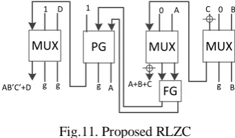
The leading zeros of the mantissa are counted using our RLZCU, the output of which is connected to the both the shift amount input of a (32, 5) reversible left barrel shifter and the minuend input of a reversible subtractor. We used three MUX gates, a PG and a FG to design the RLZC. Fig. 11 shows the circuit, and Table.2 compares this design with the existing designs.
MUX C 0 PG MUX 0 A MUX B B g A+B+C FG 1 A g 1 D g g AB’C’+D
Fig.11. Proposed RLZC
Table(2). Comparison between Proposed and Existing RLZCs
RLZC QC GO CI
Existing design in[16] 27 10 8 Existing design in[17] 20 4 4 Proposed design 17 4 4
While previous designs used barrel shifters designed in [21], [22], we used the design in Fig. 12 to apply conditional shifter and the circuit in [23] for the left barrel shifter. Also, we used the design of the [17] for RFS.
The reversible normalization has a 32-bits output, but only 23-bits are needed; therefore, in the last phase we discarded the other 9-bits.
FRG
On-1 In-1 In
Sign FRG On-2 In-2 FRG O1 I1 FRG O0 I0 …..
….. G
G
Copyright © 2015 CTTS.IN, All right reserved
5. C
OMPARISONIn this section, we analyzed the performance of the proposed design and compared it with the existing designs in [16] and [17]. Quantum cost, garbage output and constant input for each design are shown in Table 3.
6. C
ONCLUSIONA
NDF
UTUREW
ORKIn this work, we presented a reversible floating-point adder design, because the fixed-point adder is less precise in the representation of numbers. The proposed design is
made up of several parts, including: Conditional swap, Alignment unit, Converter, Addition and Normalization. We attempted to improve the parameters of quantum cost, garbage outputs and constant inputs for these parts and finally compared this design with the existing designs. Our proposed design has reduced 78% and 30% of the quantum cost, 78% and 26% of the garbage output and 79% and 30% of the constant input in compared with [16] and [17] respectively.
Table (3).Comparison between proposed design and existing designs
Stage Existing design[16] Existing design[17] Proposed design
QC GO CI QC GO CI QC GO CI
Swap 238 19 27 220 0 9 220 0 9
Alignment 12312 2260 2022 2295 388 359 1091 295 241
Addition 166 55 28 166 55 28 166 55 28
Conversion 454 94 94 345 96 90 452 88 88
Normalization 2009 498 484 1736 312 305 1414 188 186
Rounding 0 9 0 0 9 0 0 9 0
Total 15179 2935 2655 4762 860 791 3316 635 552
A
CKNOWLEDGMENTThis study was done in the Department of Computer Engineering, Dezful Branch, Islamic Azad University, Dezful, Iran and was a part of thesis of Miss Fatemeh Alaghemand a MSc. Student of Computer engineering. Authors gratefully acknowledge the help and support of Dezful Branch, Islamic Azad University, Dezful, Iran.
C
ONFLICT OFI
NTERESTThere is no conflict of interest to be declared.
R
EFERENCES1. Haghparast, M., Mohammadi, M., Navi, K., Eshghi, M., Optimized reversible multiplier circuit. Journal of Circuits, Systems, and Computers,18(02), 311-323,2009.
2. Landauer, R., Irreversibility and heat generation in the computing process. IBM journal of research and development, 5(3), 183-191,1961.
3. Bennett, C. H., Logical reversibility of computation. IBM journal of Research and Development, 17(6), 525-532, 1973.
4. Raghu kanth, B., Murali Krishna, B., Sridhar, M.,Santhi Swaroop , V.G. , A distinguish between reversible and conventional logic gates. International Journal of Engineering Research and Applications (IJERA), 2(2), 148-151, 2012. 5. Garipelly, R., Kiran, P. M., Kumar, A. S. , A
Review on Reversible Logic Gates and their Implementation. International Journal of Emerging Technology and Advanced Engineering Volume, 3, 2013.
6. Haghparast, M., K. Navi, K., A novel reversible full adder circuit for nanotechnology based
systems. Journal of Applied Sciences, 7, 3995-4000, 2007.
7. Shiri, M., Haghparast, M.,Design of the efficient nanometric reversible subtractor circuit. Research Journal of Applied Sciences, Engineering and Technology, 4(22), 4561-4565, 2012a.
8. Shiri, M., Haghparast, M., Shahbazi , V.,A novel nanometric fault tolerant reversible Subtractor circuit. Research Journal of Applied Sciences, Engineering and Technology, 4(22), 4566-4571, 2012b.
9. Feynman, R. P., Quantum mechanical computers. Foundations of physics, 16(6), 507-531, 1986.
10. Toffoli, T., Reversible computing (pp. 632-644).Springer Berlin Heidelberg, 1980.
11. Peres, A., Reversible logic and quantum computers. Physical review A,32(6), 3266,1985. 12. Fredkin, E., Toffoli, T., Conservative logic (pp.
47-81).Springer London, 2002.
13. Mohammadi, M., Eshghi, M., Haghparast, M., Bahrololoom, A., Design and optimization of reversible BCD adder/subtractor circuit for quantum and nanotechnology based systems. World Applied Sciences Journal, 4(6), 787-792, 2008.
14. Gupta, A., Singla, P., Gupta, J., Maheshwari, N.,An Improved Structure Of Reversible Adder And Subtractor. arXiv preprint arXiv:1306.1889, 2013.
15. Haghparast, M., Navi, K., A novel reversible BCD adder for nanotechnology based systems. American Journal of Applied Sciences, 5(3), 282, 2008a.
Copyright © 2015 CTTS.IN, All right reserved architecture. In Nanotechnology (IEEE-NANO),
2011 11th IEEE Conference on (pp. 451-456).IEEE, August, 2011.
17. Nguyen, T. D., Van Meter, R., A Space-Efficient Design for Reversible Floating Point Adder in Quantum Computing. arXiv preprint arXiv:1306.3760, 2013.
18. Haghparast, M., Jassbi, S. J., Navi, K., Hashemipour, O., Design of a novel reversible multiplier circuit using HNG gate in nanotechnology. In World Appl. Sci. J, 2008b. 19. Hung, W., Song, X., Yang, G., Yang,
J.,Perkowski, M., Optimal synthesis of multiple output Boolean functions using a set of quantum gates by symbolic reachability analysis. Computer-Aided Design of Integrated Circuits and Systems, IEEE Transactions on, 25(9), 1652-1663, 2006.
20. HosseiniNia, N., Design of an optimized reversible ternary and binary bidirectional and. normalization barrel shifters for floating point arithmetic. Life Sciences Journal, 9(3), 1904-1915, 2012.
21. Gorgin, S., Kaivani, A., Reversible barrel shifters.In Computer Systems and Applications, 2007.AICCSA'07. IEEE/ACS International Conference on (pp. 479-483). IEEE, May, 2007. 22. Hashmi, I., Babu, H. M. H., An efficient design of
a reversible barrel shifter. In VLSI Design, 2010.VLSID'10. 23rd International Conference on(pp. 93-98). IEEE, January, 2010.