Adv. Radio Sci., 11, 197–206, 2013 www.adv-radio-sci.net/11/197/2013/ doi:10.5194/ars-11-197-2013
© Author(s) 2013. CC Attribution 3.0 License.
Advances in
Radio Science
Simulation of RF MEMS based matching networks and a single pole
double throw switch for Multiband T/R Modules
S. A. Figur1, F. van Raay2, R. Quay2, L. Vietzorreck3, and V. Ziegler1
1EADS Deutschland GmbH, EADS Innovation Works Germany, 81663 M¨unchen, Germany 2Fraunhofer Institute of Applied Solid-State Physics (IAF), Tullastr. 72, 79108 Freiburg, Germany 3TU M¨unchen, Arcisstr. 21, 80333 M¨unchen, Germany
Correspondence to: S. A. Figur ([email protected]), F. van Raay ([email protected]),
R. Quay ([email protected]), L. Vietzorreck ([email protected]), and V. Ziegler ([email protected])
Abstract. This work presents concepts and designs for two essential components of a frequency agile transmit and re-ceive module based on Radio Frequency Micro Electro Me-chanical System (RF MEMS) switches for the frequency range from 3.5 GHz up to 8.5 GHz. The advantages of a variable power amplifier (PA) matching compared to a fixed broadband solution are examined and discussed in context with the designed components.
To demonstrate the principle functionality, an assembly concept is presented, which allows for the integration of a frequency agile 6 W power amplifier with surrounding com-ponents like phase shifters, switches and antennas. An RF MEMS switching element is introduced as a high isolation polarization switch, featuring low insertion loss as well as almost no DC power consumption.
1 Introduction
The general trend towards higher data throughput, frequency-agility as well as higher power together with higher efficiency, demands for more broadband and more flexible systems. Furthermore reconfigurability becomes an important factor to adapt to changing requirements during lifetime of a given system. In many systems, in special space borne systems, adjustments during lifetime can only be done, if these adjustments have already been foreseen and prepared during design stage and assembly.
Figure 1 depicts a frequency-agile transmit and receive module (T/R module), used in non-frequency-agile systems amended by reconfigurable components to deal with chang-ing demands. The schang-ingle components shall not be described in depth here, since in this paper the main focus lies on the
power amplifier and high-power ultra-wide-band polariza-tion switch.
With a fixed broadband matching network, compromises have to be accepted due to the Fano-Bode-criteria (see Sect. 2.2.1): the transistor cannot be optimally matched for all operating frequencies and conditions at a time. In con-trast to the common method to match a transistor over a wide frequency range, trading bandwidth for good matching, this paper presents a multi-band concept to match the transistor optimally based on the current operating situation. Adaptive multi-band matching offers the possibility to operate the am-plifier more flexibly, while choosing the situationaly best fit-ting state.
Figure 1.2 shows a schematic power amplifier based on a gallium nitride transistor (GaN), which is matched vari-ably by radio frequency micro electro mechanical system (RF MEMS) switches. Similar systems based on different technologies were presented in (Malmqvist, 2009; Qiao et al., 2005; Lu et al., 2003). Due to the almost zero DC power consumption and low insertion losses (Siegel et al., 2006), RF MEMS are well suited for applications in efficient sys-tems as well as in power amplifiers. The used RF MEMS technology is described in detail in Siegel et al. (2006).
Fig. 1. Frequency-agile T/R module. The figure depicts a single module, the complete system generally consists of an array of several single
modules.
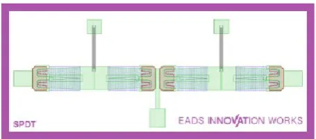
Fig. 2. Single pole double throw (SPDT) switch. Input at bottom
side, outputs left and right hand side of the layout, control lines at top.
for a fixed frequency is only possible with adaptive matching networks.
Based on the frequency bands of common communica-tion applicacommunica-tions, the frequency range between 3.7 GHz and 8.4 GHz was chosen for demonstration purposes, while the range from 1.5 GHz up to 18.1 GHz is considered to be the target specification for further development.
2 Design of single components
2.1 High-power ultra-wide-band polarization switch
An elementary part of a frequency-agile and reconfigurable T/R module, such as shown in Fig. 1 is a switching element, which can switch between the vertically or horizontally po-larized antennas. This element is also necessary to change between transmit and receive mode by changing the way the vertical signal path in Fig. 1.1 is connected with the rest of the module, adjusting magnitude and phase of the signal. Fig-ure 2 depicts an RF MEMS based single pole double throw (SPDT) switch, which can be fabricated on silicon and inte-grated in a module.
The simulation results of this switch are given in Fig. 3. These simulations do not consider any external wiring such
as bond wires or pads, since the external wiring has a strong influence on the performance and is itself strongly depending on the integration environment of the switch.
Insertion loss of less than 0.55 dB and a matching of lower than−10 dB over a frequency range from 4 GHz up to over 20 GHz show promising results. Within the complete target frequency range below 20 GHz isolation between the opened and the closed output is lower than−40 dB.
2.2 Frequency-agile power amplifier
2.2.1 General limitations of matching networks A well-known limit on the performance of matching net-works is given by the Fano-Bode-criteria. In Steer (2010) the Fano-Bode-criteria is simplified to
BW
ω0 ln
1
0avg
≤ π
Qload .
BW
ω0 : fractional bandwidth of the matching network in
radi-ans;0avg: average in-band reflection coefficient;Qload: qual-ity factor of load impedance.
Among other general results Steer, 2010 concludes from this:
1. A higher Qload results in a narrower bandwidth for a constant in-band average reflection coefficient.
2. Matching the load for all frequencies is only possible forQload=0.
3. With increasingQloadspecified bandwidths are increas-ingly difficult to achieve.
To cope with this restriction in multi-band applications, one can either:
– trade bandwidth for good matching in a broadband matching network
S. A. Figur et al.: Simulation of RF MEMS based matching networks 199
Fig. 3. Simulation results of the SPDT from Fig. 2.
Table 1. Discrete design frequencies of matching networks for
max-imum output power.
Maximum Output Power Frequencies in GHz
Gate 4 5 6.5 7.5∗ 8.5
Drain 4 5.5 6.5 – 8.5
∗Only in radials version.
– implement tunable narrowband matching networks. While the first two solutions have drawbacks in terms of per-formance or hardware costs and area consumed, the latter one has the potential for very good performance with mini-mum hardware and area consumption. Therefore, the follow-ing tunable matchfollow-ing networks are designed to provide opti-mum matching conditions for each frequency-band/mode of operation for the multi-band application.
2.2.2 Chosen transistor
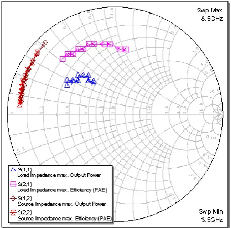
Due to the target of achieving a high output power with a single transistor, a GaN transistor was chosen. An example of a GaN based T/R module can be found in Schuh et al. (2008). The source and load impedances, which the transistor has to be connected to for frequencies between 3.5 GHz and 8.5 GHz, are shown in Fig. 4; data is given for maximum output power and maximum PAE.
Due to the position of the matching points, it can be ex-pected, that the most broadband matching can be achieved for the output matching tuned for maximum output power. The output matching network for maximum efficiency should be slightly more broadband than both input match-ings, but all three are expected to be rather narrowband.
2.2.3 Design principle of matching networks
The matching networks for gate and drain of the GaN transis-tor are realized as single stub networks on silicon. Therefore a stub line is connected in parallel at some distance to the load structure, which has to be matched to 50. The stub
Fig. 4. Large signal matching points of the chosen GaN transistor.
Data normalized to 50.
line can be realized with an open circuit at the end or can be shortcut to ground. Due to the available RF-MEMS tech-nology, the stubs have to be realized open ended. The stub represents a certain impedance to ground, based on the elec-trical length and the configuration of the stub line – in this case open ended. The distance between stub and load struc-ture is such chosen, that the parallel stub compensates for the imaginary part of the impedance seen at the stub position looking towards the load structure. Therefore a purely resis-tive impedance of 50is seen from the input of the matching network.
200 S. A. Figur et al.: Simulation of RF MEMS based matching networks
Fig. 5. Principle of a single stub matching network based on
RF-MEMS switches. Different colors and linetypes indicate different states of the matching network chosen by throwing the according switch.
stubs for matching results in varying residual line lengths be-tween currently used stub and the end of the through line towards the 50system. Since the through line is designed with an impedance of 50, the varying residual line length does not affect the matching.
Stub based matching networks, as depicted in Fig. 5, are simple to design and well suited to match the load for a few, discrete frequency points and operating modes. The three depicted examples also illustrate the limitations of the ap-proach. To avoid resonances and coupling between the stub lines, a minimum distance between two adjacent stubs has to be kept. As a result, the number of stub lines per length unit is limited.
A simple solution for this limitation is to put some stubs
λ/2 or a multiple farther away from the load structure than calculated. This increases the possible number of stubs in the design, but introduces higher losses for all possible states, due to the longer through line.
2.2.4 Frequency-agile matching networks – maximum output power
To demonstrate the capabilities of this approach, frequency agile matching networks for gate and drain have been de-signed to tune the chosen transistor for maximum output power. Table 1 gives an overview of the matched discrete frequencies. Due to geometrical restrictions, the matching networks could not be designed to match gate and drain of the transistor both at 5 GHz or 5.5 GHz. Therefore gate and drain can only be matched at two slightly different frequen-cies around 5 GHz.
Figure 6 and Fig. 7 show the designed matching networks for maximum output power. As stated before, due to the available technology, the stubs have to be realized as open circuits. Therefore, a possibly shorter shortcut stub to ground is not applicable and some stubs are rather long in Fig. 6.1.
of the approach. To avoid resonances and coupling between the stub lines, a minimum distance between two adjacent stubs has to be kept. As a result, the number of stub lines per length unit is limited.
A simple solution for this limitation is to put some stubs /2 or a multiple farther away from the load structure than calculated. This increases the possible number of stubs in the design, but introduces higher losses for all possible states, due to the longer through line.
2.2.4 Frequency-agile matching networks – maximum output power
To demonstrate the capabilities of this approach, frequency agile matching networks for gate and drain have been designed to tune the chosen transistor for maximum output power. Table 1 gives an overview of the matched discrete frequencies. Due to geometrical restrictions, the matching networks could not be designed to match gate and drain of the transistor both at 5 GHz or 5.5 GHz. Therefore gate and drain can only be matched at two slightly different frequencies around 5 GHz.
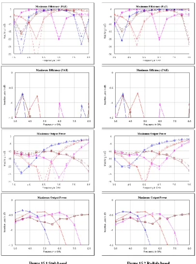
Figure 6 and Figure 7 show the designed matching networks for maximum output power. As stated before, due to the available technology, the stubs have to be realized as open circuits. Therefore, a possibly shorter shortcut stub to ground is not applicable and some stubs are rather long in Figure 6.1.
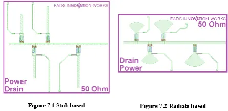
Figure 6.1Stub based Figure 6.2 Radials based
Figure 6 Gate matching network for maximum output power. The blue bar indicates the right hand side line length of the stub based network, the red, thinner bar shows the additional line length necessary for the radials based network.
Another possibility to reduce the size of the matching networks incorporates radial stubs as shown in Figure 6.2 and Figure 7.2. The higher capacity to ground of the radial stubs decreases the length and can reduce space consumption. A major drawback of this solution is the increased width of the stubs, further decreasing the number of possible stubs per length unit. In Figure 6.2 on the right hand side of the matching network, a piece of line (indicated by thin, red bar) had to be added to cope with the wide radial stubs. However, the necessity of adding additional line lengths is strongly dependent on the design. In Figure 7.2 no adjustments were necessary.
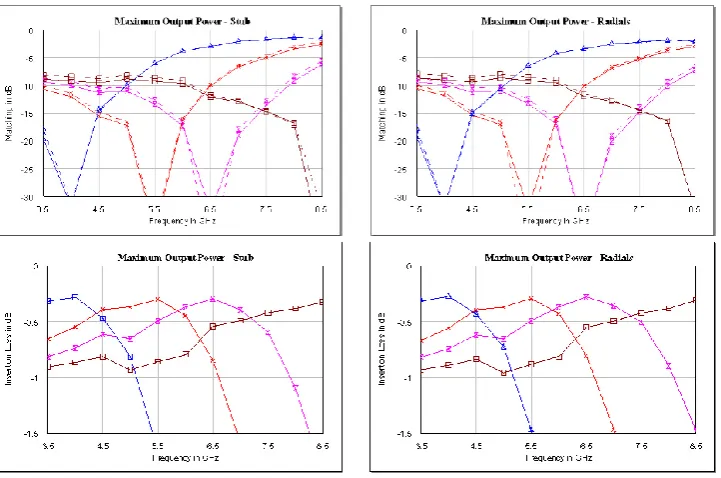
Simulation results of the gate and drain matching networks are given in
Figure 8 and Figure 9, respectively. The long stub lines of the stub based gate network result in higher insertion losses and limit the area of the smith chart, which can be matched well. In consequence matching is partially low, which could be significantly improved by using radial stubs.
Since the gate matching is rather narrowband, the frequency range around 7.5 GHz cannot be matched with one of the four states in the stub version. Consequently another stub has been added in the radial stub version to match the gate around 7.5 GHz. At the five design frequencies matching is below -10 dB and insertion loss is still high, but acceptable, since this can be compensated by a driver amplifier.
Fig. 6. Gate matching network for maximum output power. The
blue bar indicates the right hand side line length of the stub based network, the red, thinner bar shows the additional line length nec-essary for the radials based network.
Another possibility to reduce the size of the matching net-works incorporates radial stubs as shown in Fig. 6.2 and Fig. 7.2. The higher capacity to ground of the radial stubs decreases the length and can reduce space consumption. A major drawback of this solution is the increased width of the stubs, further decreasing the number of possible stubs per length unit. In Fig. 6.2 on the right hand side of the matching network, a piece of line (indicated by thin, red bar) had to be added to cope with the wide radial stubs. However, the neces-sity of adding additional line lengths is strongly dependent on the design. In Fig. 7.2 no adjustments were necessary.
Simulation results of the gate and drain matching networks are given in Fig. 8 and Fig. 9, respectively. The long stub lines of the stub based gate network result in higher inser-tion losses and limit the area of the smith chart, which can be matched well. In consequence matching is partially low, which could be significantly improved by using radial stubs. Since the gate matching is rather narrowband, the fre-quency range around 7.5 GHz cannot be matched with one of the four states in the stub version. Consequently another stub has been added in the radial stub version to match the gate around 7.5 GHz. At the five design frequencies matching is below−10 dB and insertion loss is still high, but acceptable, since this can be compensated by a driver amplifier.
S. A. Figur et al.: Simulation of RF MEMS based matching networks 201
Fig. 7. Drain matching network for maximum output power.
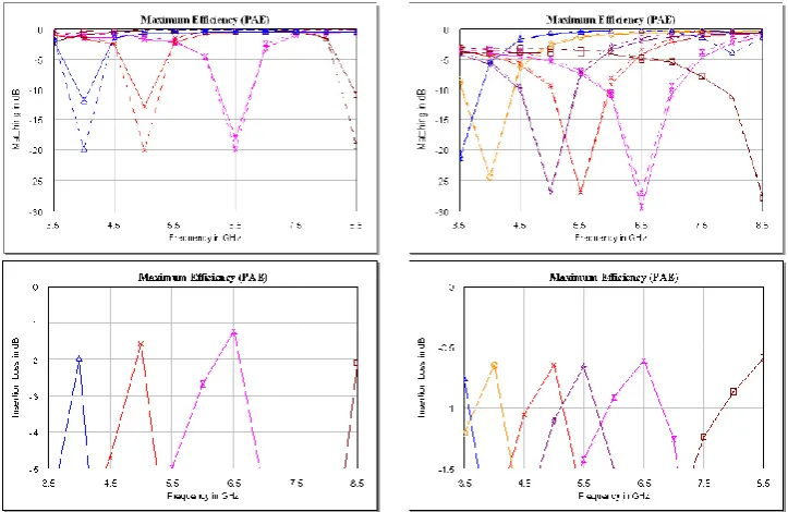
2.2.5 Frequency-agile matching networks – maximum PAE
Additional to the networks shown in Sect. 2.2.4, matching networks for maximum PAE have been designed. Since the design principle is the same, only the smaller radial versions are shown here. The layout is depicted in Fig. 10.
The matching is, as expected to be, more narrowband than shown for the maximum output power networks. Figure 11 gives the simulation results of these structures. Due to the low space consumption of the radial stubs in Fig. 10.2, ad-ditional stubs could be added to achieve a better average matching over the whole frequency range. The gate match-ing network has not been extended to keep the losses as low as possible. The corresponding design frequencies for both matching networks are given in Table 2.
The drain matching works quite well over a wide fre-quency range, exhibiting losses lower than 1 dB. However, the performance of the gate matching network is comparable to the one shown in Fig. 8 for maximum output power mode.
2.2.6 Combined mode frequency-agile matching networks
The formerly shown networks are designed to demonstrate the frequency-agility of this concept. As stated before, a ma-jor advantage of adjustable matching networks is the possi-bility to change the operating mode of the transistor during operation. Therefore a combined matching network, based on the single matching networks for maximum output power and maximum PAE, has been designed to show this function-ality.
In Table 3 design frequencies for maximum output power and maximum PAE are summarized. The necessary source impedances for maximum output power and maximum PAE are not very different for the gate matching. Therefore the combined matching network is only designed for drain matching.
The according designs as stub based and partially radials based are depicted in Fig. 12. The two remaining line stubs in Fig. 12.2 could not be replaced with radials, since the radials would have been so big, that these would have been
overlap-Table 2. Discrete design frequencies of radials based matching
net-works for maximum PAE.
Maximum PAE Frequencies in GHz
Gate – 4 5 – 6.5 8.5
Drain 3.5 4 5 5.5 6.5 8.5
Table 3. Discrete design frequencies of combined matching
net-work.
Drain Frequencies in GHz
Maximum Efficiency (PAE) 4 5 6.5 8.5 Maximum Output Power 4 5.5 6.5 8.5
ping in any possible configuration. Therefore the two stubs have been kept. Furthermore the additional design frequen-cies of the drain matching network for maximum PAE had to be discarded, due to the high number of stubs, which had to be arranged.
Figure 15.1 and Fig. 15.2 depict simulation results of the combined matching network for stub based and radials based realizations, respectively. Both versions are quite similar and show very good performance.
The maximum output power states are close to the re-sults shown before, even though insertion loss is a bit higher, due to the additional stubs and therefore longer through line. The optimum load impedance for maximum PAE is varying more over frequency than the one for maximum output power and exhibiting a higher quality factor. As a direct result, the matching of the four discrete states is narrower, than the one for maximum output power. However, the matching is good for the design frequencies and insertion loss is acceptable.
3 Integration approach
In a later design step the power amplifier shall be integrated in a T/R module as depicted in Fig. 1. Figure 13 gives a top view of the integration approach, restricted to the close sur-rounding of the power amplifier.
In agreement with the manufacturer of the GaN transistor, the integration approach in Fig. 14 has been worked out. The basis of this approach is a conductive carrier board, provid-ing a common ground plane. To keep the bond wires as short as possible, it is accepted, that the ground plane is not flat but contains a small step around the transistor. This is neces-sary, due to the different chip thicknesses of silicon matching networks and GaN transistor.
Fig. 8. Simulation results of gate matching networks for maximum output power – stub and radials based versions. Different colors and
symbols denote different states of the networks. Matching graphs includeS11 (dashed line) as well as S22 (solid line). Insertion Loss showsS21andS12, which are identical.
Fig. 9. Simulation results of drain matching networks for maximum output power – stub and radials based versions. Different colors and
S. A. Figur et al.: Simulation of RF MEMS based matching networks 203
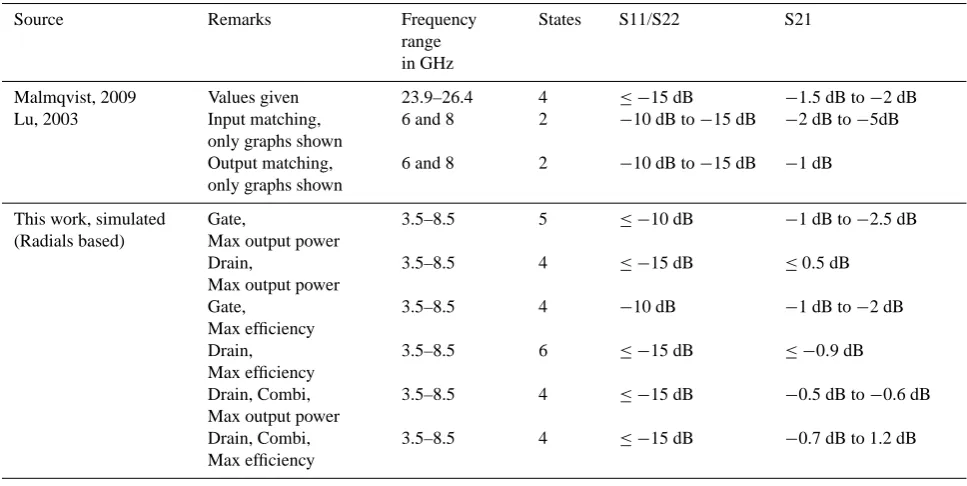
Table 4. Comparison with presented measurements of other groups.
Source Remarks Frequency
range in GHz
States S11/S22 S21
Malmqvist, 2009 Values given 23.9–26.4 4 ≤ −15 dB −1.5 dB to−2 dB
Lu, 2003 Input matching,
only graphs shown
6 and 8 2 −10 dB to−15 dB −2 dB to−5dB
Output matching, only graphs shown
6 and 8 2 −10 dB to−15 dB −1 dB
This work, simulated (Radials based)
Gate,
Max output power
3.5–8.5 5 ≤ −10 dB −1 dB to−2.5 dB
Drain,
Max output power
3.5–8.5 4 ≤ −15 dB ≤0.5 dB
Gate,
Max efficiency
3.5–8.5 4 −10 dB −1 dB to−2 dB
Drain, Max efficiency
3.5–8.5 6 ≤ −15 dB ≤ −0.9 dB
Drain, Combi, Max output power
3.5–8.5 4 ≤ −15 dB −0.5 dB to−0.6 dB
Drain, Combi, Max efficiency
3.5–8.5 4 ≤ −15 dB −0.7 dB to 1.2 dB
Fig. 10. Radials based matching networks for gate and drain,
opti-mized for maximum efficiency (PAE).
The Rogers RT/Duroid 5880 PCBs are fabricated in a thickness similar to the silicon chips. Thus the top sides of the silicon based matching networks and the PCBs are lev-eled without the necessity to mill steps into the conductive carrier. Milling tolerances for the conductive carrier could cause additional spacing between neighboring structures, re-sulting in longer bondwires. Additional surrounding compo-nents can be integrated in the same way or on top of the Rogers RT/Duroid 5880 PCBs.
4 Comparison with state of the art
A comparison with other works is difficult, since this kind of matching network is specifically designed for one tran-sistor. Therefore generally the system’s overall performance is shown and the performance of the matching network
it-self is not presented. Two similar works have been found, which give results on the matching networks. The main re-sults given are summarized in Table 4 and compared with this work.
5 Conclusions
This paper shows the design of an RF-MEMS SPDT switch for agile systems as well as adaptive frequency-agile matching networks for adaptively matching power am-plifiers to the current operating conditions. The presented simulation results promise a valuable benefit of adaptive matching networks compared to fixed matching networks in multi-band applications.
Apart from overcoming compromises necessary for broad-band matching networks, the adaptive frequency-agile matching networks proposed in this paper, can tune the tran-sistor between different operational modes, while keeping the operating frequency fixed. Therefore an amplifier can be tuned from maximum output power to maximum PAE, de-pending on current conditions. This feature is interesting for efficient systems, which are in non-constant environments. If propagation attenuation increases, the transistor can be tuned from maximum PAE mode to maximum output power to compensate for the higher losses. When the attenuation de-creases, the mode can be changed back to maximum PAE to save energy.
Fig. 11. Simulation results of gate and drain matching networks for maximum efficiency (PAE) – radials based. Different colors and symbols
denote different states of the networks. Matching graphs includeS11(dashed line) as well asS22(solid line). Insertion Loss showsS21and S12, which are identical.
Fig. 12. Combined drain matching network. Transistor can be tuned
for maximum output power or maximum efficiency (PAE).
Fig. 13. Schematic integration approach in top view.
Fig. 14. Schematic integration approach in cross section.
6 Outlook
S. A. Figur et al.: Simulation of RF MEMS based matching networks 205
Fig. 15. Simulation results of combined matching network for maximum output power and maximum efficiency (PAE) – stub and radial
Acknowledgements. This work has been financially supported by FP7 – Space, Project Saturne, Grant agreement no. 242458.
References
Lu, Y., Peroulis, D., Mohammadi, S., and Katehi, L. P. B.: A MEMS Reconfigurable Matching Network for a Class AB Amplifier, IEEE Microwave and Wireless Components Letters, 13, 437– 439, 2003.
Malmqvist, R., Rantakari, P., Samuelsson, C., Lahti, M., Cheng, S., Saijets, J., Vaha-Heikkila, T., Rydberg, A., and Varis, J.: RF MEMS based impedance matching networks for tunable multi-band microwave low noise amplifiers, Semiconductor Confer-ence, 2009, CAS 2009, International, vol. 1, October 2009.
Qiao, D., Molfino, R., Lardizabal, S. M., Pillans, B., Asbeck, P. M., and Jerinic, G.: An Intelligently Controlled RF Power Amplifier With a Reconfigurable MEMS-Varactor Tuner, Transactions on Microwave Theory and Techniques, 53, 1089–1095, 2005. Schuh, P., Sledzik, H., Reber, R., Fleckenstein, A., Leberer, R.,
Op-permann, M., Quay, R., van Raay, F., Seelmann-Eggebert, M., Kiefer, R., and Mikulla, M.: GaN MMIC based T/R-Module Front-End for X-Band Applications, Microwave Integrated Cir-cuit Conference, 2008, EuMIC 2008, European, 27–28 October 2008.
Siegel, C., Ziegler, V., Schonlinner, B., Prechtel, U., and Schu-macher, H.: Simplified RF-MEMS switches using implanted conductors and thermal oxide, 36th European Microwave Con-ference, September 2006.