COMPLETE
DIGITAL DESIGN
A Comprehensive Guide to Digital Electronics
and Computer System Architecture
Mark Balch
McGRAW-HILL
New York Chicago San Francisco Lisbon London Madrid Mexico CityMilan
New Delhi San Juan Seoul Singapore Sydney Toronto
Copyright © 2003 by The McGraw-Hill Companies, Inc. All rights reserved. Manufactured in the United States of America. Except as permitted under the United States Copyright Act of 1976, no part of this publication may be reproduced or distributed in any form or by any means, or stored in a database or retrieval system, without the prior written permission of the publisher.
0-07-143347-3
The material in this eBook also appears in the print version of this title: 0-07-140927-0
All trademarks are trademarks of their respective owners. Rather than put a trademark symbol after every occur-rence of a trademarked name, we use names in an editorial fashion only, and to the benefit of the trademark owner, with no intention of infringement of the trademark. Where such designations appear in this book, they have been printed with initial caps.
McGraw-Hill eBooks are available at special quantity discounts to use as premiums and sales promotions, or for use in corporate training programs. For more information, please contact George Hoare, Special Sales, at [email protected] or (212) 904-4069.
TERMS OF USE
This is a copyrighted work and The McGraw-Hill Companies, Inc. (“McGraw-Hill”) and its licensors reserve all rights in and to the work. Use of this work is subject to these terms. Except as permitted under the Copyright Act of 1976 and the right to store and retrieve one copy of the work, you may not decompile, disassemble, reverse engineer, reproduce, modify, create derivative works based upon, transmit, distribute, disseminate, sell, publish or sublicense the work or any part of it without McGraw-Hill’s prior consent. You may use the work for your own noncommercial and personal use; any other use of the work is strictly prohibited. Your right to use the work may be terminated if you fail to comply with these terms.
THE WORK IS PROVIDED “AS IS”. McGRAW-HILL AND ITS LICENSORS MAKE NO GUARANTEES OR WARRANTIES AS TO THE ACCURACY, ADEQUACY OR COMPLETENESS OF OR RESULTS TO BE OBTAINED FROM USING THE WORK, INCLUDING ANY INFORMATION THAT CAN BE ACCESSED THROUGH THE WORK VIA HYPERLINK OR OTHERWISE, AND EXPRESSLY DISCLAIM ANY WAR-RANTY, EXPRESS OR IMPLIED, INCLUDING BUT NOT LIMITED TO IMPLIED WARRANTIES OF MERCHANTABILITY OR FITNESS FOR A PARTICULAR PURPOSE. McGraw-Hill and its licensors do not warrant or guarantee that the functions contained in the work will meet your requirements or that its operation will be uninterrupted or error free. Neither McGraw-Hill nor its licensors shall be liable to you or anyone else for any inaccuracy, error or omission, regardless of cause, in the work or for any damages resulting therefrom. McGraw-Hill has no responsibility for the content of any information accessed through the work. Under no cir-cumstances shall McGraw-Hill and/or its licensors be liable for any indirect, incidental, special, punitive, conse-quential or similar damages that result from the use of or inability to use the work, even if any of them has been advised of the possibility of such damages. This limitation of liability shall apply to any claim or cause whatso-ever whether such claim or cause arises in contract, tort or otherwise.
DOI: 10.1036/0071433473
CONTENTS
Preface xiii
Acknowledgments xix
PART 1
Digital Fundamentals
Chapter 1 Digital Logic . . . .3 1.1 Boolean Logic / 3
1.2 Boolean Manipulation / 7 1.3 The Karnaugh map /8
1.4 Binary and Hexadecimal Numbering /10 1.5 Binary Addition / 14
1.6 Subtraction and Negative Numbers / 15 1.7 Multiplication and Division / 17 1.8 Flip-Flops and Latches / 18 1.9 Synchronous Logic /21
1.10 Synchronous Timing Analysis / 23 1.11 Clock Skew /25
1.12 Clock Jitter / 27
1.13 Derived Logical Building Blocks / 28
Chapter 2 Integrated Circuits and the 7400 Logic Families. . . .33 2.1 The Integrated Circuit / 33
2.2 IC Packaging / 38
2.3 The 7400-Series Discrete Logic Family / 41 2.4 Applying the 7400 Family to Logic Design / 43 2.5 Synchronous Logic Design with the 7400 Family / 45 2.6 Common Variants of the 7400 Family /50
2.7 Interpreting a Digital IC Data Sheet /51
Chapter 3 Basic Computer Architecture . . . .55 3.1 The Digital Computer /56
3.2 Microprocessor Internals /58 3.3 Subroutines and the Stack /60 3.4 Reset and Interrupts /62
3.5 Implementation of an Eight-Bit Computer / 63 3.6 Address Banking /67
3.7 Direct Memory Access /68
3.8 Extending the Microprocessor Bus / 70 3.9 Assembly Language and Addressing Modes /72 -Balch.book Page vii Thursday, May 15, 2003 3:46 PM
For more information about this title, click here.
viii CONTENTS
Chapter 4 Memory. . . .77 4.1 Memory Classifications / 77
4.2 EPROM /79 4.3 Flash Memory /81 4.4 EEPROM /85
4.5 Asynchronous SRAM / 86 4.6 Asynchronous DRAM / 88 4.7 Multiport Memory / 92 4.8 The FIFO / 94
Chapter 5 Serial Communications . . . .97 5.1 Serial vs. Parallel Communication / 98
5.2 The UART / 99
5.3 ASCII Data Representation / 102 5.4 RS-232 / 102
5.5 RS-422 / 107
5.6 Modems and Baud Rate / 108 5.7 Network Topologies / 109 5.8 Network Data Formats /110 5.9 RS-485 / 112
5.10 A Simple RS-485 Network / 114 5.11 Interchip Serial Communications / 117
Chapter 6 Instructive Microprocessors and Microcomputer Elements . . . .121 6.1 Evolution / 121
6.2 Motorola 6800 Eight-bit Microprocessor Family /122 6.3 Intel 8051 Microcontroller Family / 125
6.4 Microchip PIC® Microcontroller Family / 131 6.5 Intel 8086 16-Bit Microprocessor Family / 134 6.6 Motorola 68000 16/32-Bit Microprocessor Family / 139
PART 2
Advanced Digital Systems
Chapter 7 Advanced Microprocessor Concepts . . . .145 7.1 RISC and CISC /145
7.2 Cache Structures / 149 7.3 Caches in Practice / 154
7.4 Virtual Memory and the MMU / 158
7.5 Superpipelined and Superscalar Architectures / 161 7.6 Floating-Point Arithmetic / 165
7.7 Digital Signal Processors /167 7.8 Performance Metrics / 169
Chapter 8 High-Performance Memory Technologies. . . .173 8.1 Synchronous DRAM /173
CONTENTS ix
Chapter 9 Networking. . . .193 9.1 Protocol Layers One and Two /193
9.2 Protocol Layers Three and Four / 194 9.3 Physical Media / 197
9.4 Channel Coding / 198 9.5 8B10B Coding / 203 9.6 Error Detection /207 9.7 Checksum /208
9.8 Cyclic Redundancy Check /209 9.9 Ethernet /215
Chapter 10 Logic Design and Finite State Machines . . . .221 10.1 Hardware Description Languages /221
10.2 CPU Support Logic / 227 10.3 Clock Domain Crossing / 233 10.4 Finite State Machines / 237 10.5 FSM Bus Control /239 10.6 FSM Optimization /243 10.7 Pipelining / 245
Chapter 11 Programmable Logic Devices . . . .249 11.1 Custom and Programmable Logic /249
11.2 GALs and PALs /252 11.3 CPLDs /255 11.4 FPGAs /257
PART 3
Analog Basics for Digital Systems
Chapter 12 Electrical Fundamentals . . . .267 12.1 Basic Circuits / 267
12.2 Loop and Node Analysis / 268 12.3 Resistance Combination / 271 12.4 Capacitors / 272
12.5 Capacitors as AC Elements / 274 12.6 Inductors / 276
12.7 Nonideal RLC Models / 276 12.8 Frequency Domain Analysis / 279 12.9 Lowpass and Highpass Filters / 283 12.10 Transformers /288
Chapter 13 Diodes and Transistors . . . .293 13.1 Diodes /293
x CONTENTS
Chapter 14 Operational Amplifiers . . . .311 14.1 The Ideal Op-amp / 311
14.2 Characteristics of Real Op-amps / 316 14.3 Bandwidth Limitations /324 14.4 Input Resistance / 325
14.5 Summation Amplifier Circuits / 328 14.6 Active Filters / 331
14.7 Comparators and Hysteresis / 333
Chapter 15 Analog Interfaces for Digital Systems . . . .339 15.1 Conversion between Analog and Digital Domains / 339
15.2 Sampling Rate and Aliasing /341 15.3 ADC Circuits /345
15.4 DAC Circuits /348
15.5 Filters in Data Conversion Systems / 350
PART 4
Digital System Design in Practice
Chapter 16 Clock Distribution . . . .355 16.1 Crystal Oscillators and Ceramic Resonators / 355
16.2 Low-Skew Clock Buffers / 357 16.3 Zero-Delay Buffers: The PLL / 360 16.4 Frequency Synthesis / 364 16.5 Delay-Locked Loops /366 16.6 Source-Synchronous Clocking / 367
Chapter 17 Voltage Regulation and Power Distribution . . . .371 17.1 Voltage Regulation Basics / 372
17.2 Thermal Analysis / 374
17.3 Zener Diodes and Shunt Regulators / 376 17.4 Transistors and Discrete Series Regulators / 379 17.5 Linear Regulators / 382
17.6 Switching Regulators / 386 17.7 Power Distribution / 389 17.8 Electrical Integrity / 392
Chapter 18 Signal Integrity. . . .397 18.1 Transmission Lines /398
18.2 Termination / 403 18.3 Crosstalk / 408
18.4 Electromagnetic Interference / 410
18.5 Grounding and Electromagnetic Compatibility / 413 18.6 Electrostatic Discharge / 415
Chapter 19 Designing for Success . . . .419 19.1 Practical Technologies / 420
CONTENTS xi
19.3 Manually Wired Circuits / 425 19.4 Microprocessor Reset /428 19.5 Design for Debug / 429 19.6 Boundary Scan /431 19.7 Diagnostic Software / 433 19.8 Schematic Capture and Spice / 436 19.9 Test Equipment / 440
Appendix A
Further Education. . . .443
Index 445
PREFACE
Digital systems are created to perform data processing and control tasks. What distinguishes one system from another is an architecture tailored to efficiently execute the tasks for which it was de-signed. A desktop computer and an automobile’s engine controller have markedly different attributes dictated by their unique requirements. Despite these differences, they share many fundamental building blocks and concepts. Fundamental to digital system design is the ability to choose from and apply a wide range of technologies and methods to develop a suitable system architecture. Digital electronics is a field of great breadth, with interdependent topics that can prove challenging for indi-viduals who lack previous hands-on experience in the field.
This book’s focus is explaining the real-world implementation of complete digital systems. In do-ing so, the reader is prepared to immediately begin design and implementation work without bedo-ing left to wonder about the myriad ancillary topics that many texts leave to independent and sometimes painful discovery. A complete perspective is emphasized, because even the most elegant computer architecture will not function without adequate supporting circuits.
A wide variety of individuals are intended to benefit from this book. The target audiences include
•
Practicing electrical engineers seeking to sharpen their skills in modern digital system design.Engineers who have spent years outside the design arena or in less-than-cutting-edge areas often find that their digital design skills are behind the times. These professionals can acquire directly relevant knowledge from this book’s practical discussion of modern digital technologies and de-sign practices.
•
College graduates and undergraduates seeking to begin engineering careers in digital electronics.College curricula provide a rich foundation of theoretical understanding of electrical principles and computer science but often lack a practical presentation of how the many pieces fit together in real systems. Students may understand conceptually how a computer works while being incapable of actually building one on their own. This book serves as a bridge to take readers from the theo-retical world to the everyday design world where solutions must be complete to be successful.
•
Technicians and hobbyists seeking a broad orientation to digital electronics design. Some people have an interest in understanding and building digital systems without having a formal engineer-ing degree. Their need for practical knowledge in the field is as strong as for degreed engineers, but their goals may involve laboratory support, manufacturing, or building a personal project.There are four parts to this book, each of which addresses a critical set of topics necessary for successful digital systems design. The parts may be read sequentially or in arbitrary order, depend-ing on the reader’s level of knowledge and specific areas of interest.
A complete discussion of digital logic and microprocessor fundamentals is presented in the first part, including introductions to basic memory and communications architectures. More advanced computer architecture and logic design topics are covered in Part 2, including modern microproces-sor architectures, logic design methodologies, high-performance memory and networking technolo-gies, and programmable logic devices.
-Balch.book Page xiii Thursday, May 15, 2003 3:46 PM
xiv PREFACE
Part 3 steps back from the purely digital world to focus on the critical analog support circuitry that is important to any viable computing system. These topics include basic DC and AC circuit analysis, diodes, transistors, op-amps, and data conversion techniques. The fundamental topics from the first three parts are tied together in Part 4 by discussing practical digital design issues, including clock distribution, power regulation, signal integrity, design for test, and circuit fabrication tech-niques. These chapters deal with nuts-and-bolts design issues that are rarely covered in formal elec-tronics courses.
More detailed descriptions of each part and chapter are provided below.
PART 1
DIGITAL FUNDAMENTALS
The first part of this book provides a firm foundation in the concepts of digital logic and computer architecture. Logic is the basis of computers, and computers are intrinsically at the heart of digital systems. We begin with the basics: logic gates, integrated circuits, microprocessors, and computer architecture. This framework is supplemented by exploring closely related concepts such as memory and communications that are fundamental to any complete system. By the time you have completed Part 1, you will be familiar with exactly how a computer works from multiple perspectives: individ-ual logic gates, major architectural building blocks, and the hardware/software interface. You will also have a running start in design by being able to thoughtfully identify and select specific off-the-shelf chips that can be incorporated into a working system. A multilevel perspective is critical to suc-cessful systems design, because a system architect must simultaneously consider high-level feature trade-offs and low-level implementation possibilities. Focusing on one and not the other will usually lead to a system that is either impractical (too expensive or complex) or one that is not really useful. Chapter 1, “Digital Logic,” introduces the fundamentals of Boolean logic, binary arithmetic, and flip-flops. Basic terminology and numerical representations that are used throughout digital systems design are presented as well. On completing this chapter, the awareness gained of specific logical building blocks will help provide a familiarity with supporting logic when reading about higher-level concepts in later chapters.
Chapter 2, “Integrated Circuits and the 7400 Logic Families,” provides a general orientation to in-tegrated circuits and commonly used logic ICs. This chapter is where the rubber meets the road and the basics of logic design become issues of practical implementation. Small design examples pro-vide an idea of how various logic chips can be connected to create functional subsystems. Attention is paid to readily available components and understanding IC specifications, without which chips cannot be understood and used. The focus is on design with real off-the-shelf components rather than abstract representations on paper.
Chapter 3, “Basic Computer Architecture,” cracks open the heart of digital systems by explaining how computers and microprocessors function. Basic concepts, including instruction sets, memory, address decoding, bus interfacing, DMA, and assembly language, are discussed to create a complete picture of what a computer is and the basic components that go into all computers. Questions are not left as exercises for the reader. Rather, each mechanism and process in a basic computer is discussed. This knowledge enables you to move ahead and explore the individual concepts in more depth while maintaining an overall system-level view of how everything fits together.
Chapter 4, “Memory,” discusses this cornerstone of digital systems. With the conceptual under-standing from Chapter 3 of what memory is and the functions that it serves, the discussion progresses to explain specific types of memory devices, how they work, and how they are applicable to different computing applications. Trade-offs of various memory technologies, including SRAM, DRAM, flash, and EPROM, are explored to convey an understanding of why each technology has its place in various systems.
PREFACE xv
Chapter 5, “Serial Communications,” presents one of the most basic aspects of systems design: moving data from one system to another. Without data links, computers would be isolated islands. Communication is key to many applications, whether accessing the Internet or gathering data from a remote sensor. Topics including RS-232 interfaces, modems, and basic multinode networking are discussed with a focus on implementing real data links.
Chapter 6, “Instructive Microprocessors and Microcomputer Elements,” walks through five ex-amples of real microprocessors and microcontrollers. The devices presented are significant because of their trail-blazing roles in defining modern computing architecture, as exhibited by the fact that, decades later, they continue to turn up in new designs in one form or another. These devices are used as vehicles to explain a wide range of computing issues from register, memory, and bus architectures to interrupt vectoring and operating system privilege levels.
PART 2
ADVANCED DIGITAL SYSTEMS
Digital systems operate by acquiring data, manipulating that data, and then transferring the results as dictated by the application. Part 2 builds on the foundations of Part 1 by exploring the state of the art in microprocessor, memory, communications, and logic implementation technologies. To effectively conceive and implement such systems requires an understanding of what is possible, what is practi-cal, and what tools and building blocks exist with which to get started. On completing Parts 1 and 2, you will have acquired a broad understanding of digital systems ranging from small microcontrollers to 32-bit microcomputer architecture and high-speed networking, and the logic design methodolo-gies that underlie them all. You will have the ability to look at a digital system, whether pre-existing or conceptual, and break it into its component parts—the first step in solving a problem.
Chapter 7, “Advanced Microprocessor Concepts,” discusses the key architectural topics behind modern 32- and 64-bit computing systems. Basic concepts including RISC/CISC, floating-point arithmetic, caching, virtual memory, pipelining, and DSP are presented from the perspective of what a digital hardware engineer needs to know to understand system-wide implications and design useful circuits. This chapter does not instruct the reader on how to build the fastest microprocessors, but it does explain how these devices operate and, more importantly, what system-level design consider-ations and resources are necessary to achieve a functioning system.
Chapter 8, “High-Performance Memory Technologies,” presents the latest SDR/DDR SDRAM and SDR/DDR/QDR SSRAM devices, explains how they work and why they are useful in high-per-formance digital systems, and discusses the design implications of each. Memory is used by more than just microprocessors. Memory is essential to communications and data processing systems. Un-derstanding the capabilities and trade-offs of such a central set of technologies is crucial to designing a practical system. Familiarity with all mainstream memory technologies is provided to enable a firm grasp of the applications best suited to each.
Chapter 9, “Networking,” covers the broad field of digital communications from a digital hard-ware perspective. Network protocol layering is introduced to explain the various levels at which hardware and software interact in modern communication systems. Much of the hardware responsi-bility for networking lies at lower levels in moving bits onto and off of the communications medium. This chapter focuses on the low-level details of twisted-pair and fiber-optic media, transceiver tech-nologies, 8B10B channel coding, and error detection with CRC and checksum logic. A brief presen-tation of Ethernet concludes the chapter to show how a real networking standard functions.
xvi PREFACE
means of designing synchronous and combinatorial logic. Once the basic methodology of designing logic has been discussed, common support logic solutions, including address decoding, control/sta-tus registers, and interrupt control logic, are shown with detailed design examples. Designing logic to handle asynchronous inputs across multiple clock domains is presented with specific examples. More complex logic circuits capable of implementing arbitrary algorithms are built from finite state machines—a topic explored in detail with design examples to ensure that the concepts are properly translated into reality. Finally, state machine optimization techniques, including pipelining, are dis-cussed to provide an understanding of how to design logic that can be reliably implemented.
Chapter 11, “Programmable Logic Devices,” explains the various logic implementation technolo-gies that are used in a digital system. GALs, PALs, CPLDs, and FPGAs are presented from the per-spectives of how they work, how they are used to implement arbitrary logic designs, and the capabilities and features of each that make them suitable for various types of designs. These devices represent the glue that holds some systems together and the core operational elements of others. This chapter aids in deciding which technology is best suited to each logic application and how to select the right device to suit a specific need.
PART 3
ANALOG BASICS FOR DIGITAL SYSTEMS
All electrical systems are collections of analog circuits, but digital systems masquerade as discrete bi-nary entities when they are properly designed. It is necessary to understand certain fundamental top-ics in circuit analysis so that digital circuits can be made to behave in the intended binary manner. Part 3 addresses many essential analog topics that have direct relevance to designing successful digi-tal systems. Many digidigi-tal engineers shrink away from basic DC and AC circuit analysis either for fear of higher mathematics or because it is not their area of expertise. This needn’t be the case, because most day-to-day analysis required for digital systems can be performed with basic algebra. Further-more, a digital systems slant on analog electronics enables many simplifications that are not possible in full-blown analog design. On completing this portion of the book, you will be able to apply passive components, discrete diodes and transistors, and op-amps in ways that support digital circuits.
Chapter 12, “Electrical Fundamentals,” addresses basic DC and AC circuit analysis. Resistors, ca-pacitors, inductors, and transformers are explained with straightforward means of determining volt-ages and currents in simple analog circuits. Nonideal characteristics of passive components are discussed, which is a critical aspect of modern, high-speed digital systems. Many a digital system has failed because its designers were unaware of increasingly nonideal behavior of components as operating frequencies get higher. Frequency-domain analysis and basic filtering are presented to ex-plain common analog structures and how they can be applied to digital systems, especially in mini-mizing noise, a major contributor to transient and hard-to-detect problems.
Chapter 13, “Diodes and Transistors,” explains the basic workings of discrete semiconductors and provides specific and fully analyzed examples of how they are easily applied to digital applications. LEDs are covered as well as bipolar and MOS transistors. An understanding of how diodes and tran-sistors function opens up a great field of possible solutions to design problems. Diodes are essential in power-regulation circuits and serve as voltage references. Transistors enable electrical loads to be driven that are otherwise too heavy for a digital logic chip to handle.
PREFACE xvii
Chapter 15, “Analog Interfaces for Digital Systems,” covers the basics of analog-to-digital and digital-to-analog conversion techniques. Many digital systems interact with real-world stimuli in-cluding audio, video, and radio frequencies. Data conversion is a key portion of these systems, en-abling continuous analog signals to be represented and processed as binary numbers. Several common means of performing data conversion are discussed along with fundamental concepts such as the Nyquist frequency and anti-alias filtering.
PART 4
DIGITAL SYSTEM DESIGN IN PRACTICE
When starting to design a new digital system, high-profile features such as the microprocessor and memory architecture often get most of the attention. Yet there are essential support elements that may be overlooked by those unfamiliar with them and unaware of the consequences of not taking time to address necessary details. All too often, digital engineers end up with systems that almost work. A microprocessor may work properly for a few hours and then quit. A data link may work fine one day and then experience inexplicable bit errors the next day. Sometimes these problems are the result of logic bugs, but mysterious behavior may be related to a more fundamental electrical flaw. The final part of this book explains the supporting infrastructure and electrical phenomena that must be understood to design and build reliable systems.
Chapter 16, “Clock Distribution,” explores an essential component of all digital systems: proper generation and distribution of clocks. Many common clock generation and distribution methods are presented with detailed circuit implementation examples including low-skew buffers, termination, and PLLs. Related subjects, including frequency synthesis, DLLs, and source-synchronous clock-ing, are presented to lend a broad perspective on system-level clocking strategies.
Chapter 17, “Voltage Regulation and Power Distribution” discusses the fundamental power infra-structure necessary for system operation. An introduction to general power handling is provided that covers issues such as circuit specifications and safety issues. Thermal analysis is emphasized for safety and reliability concerns. Basic regulator design with discrete components and integrated cir-cuits is explained with numerous illustrative circir-cuits for each topic. The remainder of the chapter ad-dresses power distribution topics including wiring, circuit board power planes, and power supply decoupling capacitors.
Chapter 18, “Signal Integrity,” delves into a set of topics that addresses the nonideal behavior of high-speed digital signals. The first half of this chapter covers phenomena that are common causes of corrupted digital signals. Transmission lines, signal reflections, crosstalk, and a wide variety of termination schemes are explained. These topics provide a basic understanding of what can go wrong and how circuits and systems can be designed to avoid signal integrity problems. Electromag-netic radiation, grounding, and static discharge are closely related subjects that are presented in the second half of the chapter. An overview is presented of the problems that can arise and their possible solutions. Examples illustrate concepts that apply to both circuit board design and overall system en-closure design—two equally important matters for consideration.
xviii PREFACE
analog circuit simulation. Spice applications are covered and augmented by complete examples that start with circuits, proceed with Spice modeling, and end with Spice simulation result analysis. The chapter closes with a brief overview of common test equipment that is beneficial in debugging and characterizing digital systems.
Following the main text is Appendix A, a brief list of recommended resources for further reading and self-education. Modern resources range from books to trade journals and magazines to web sites. Many specific vendors and products are mentioned throughout this book to serve as examples and as starting points for your exploration. However, there are many more companies and products than can be practically listed in a single text. Do not hesitate to search out and consider manufacturers not mentioned here, because the ideal component for your application might otherwise lie undiscovered. When specific components are described in this book, they are described in the context of the discus-sion at hand. References to component specifications cannot substitute for a vendor’s data sheet, be-cause there is not enough room to exhaustively list all of a component’s attributes, and such specifications are always subject to revision by the manufacturer. Be sure to contact the manufac-turer of a desired component to get the latest information on that product. Component manufacmanufac-turers have a vested interest in providing you with the necessary information to use their products in a safe and effective manner. It is wise to take advantage of the resources that they offer. The widespread use of the Internet has greatly simplified this task.
True proficiency in a trade comes with time and practice. There is no substitute for experience or mentoring from more senior engineers. However, help in acquiring this experience by being pointed in the right direction can not only speed up the learning process, it can make it more enjoyable as well. With the right guide, a motivated beginner’s efforts can be more effectively channeled through the early adoption of sound design practices and knowing where to look for necessary information. I sincerely hope that this book can be your guide, and I wish you the best of luck in your endeavors.
ACKNOWLEDGMENTS
On completing a book of this nature, it becomes clear to the author that the work would not have been possible without the support of others. I am grateful for the many talented engineers that I have been fortunate to work with and learn from over the years. More directly, several friends and col-leagues were kind enough to review the initial draft, provide feedback on the content, and bring to my attention details that required correction and clarification. I am indebted to Rich Chernock and Ken Wagner, who read through the entire text over a period of many months. Their thorough inspec-tion provided welcome and valuable perspectives on everything ranging from fine technical points to overall flow and style. I am also thankful for the comments and suggestions provided by Todd Gold-smith and Jim O’Sullivan, who enabled me to improve the quality of this book through their input.
I am appreciative of the cooperation provided by several prominent technology companies. Men-tor Graphics made available their ModelSim Verilog simulaMen-tor, which was used to verify the correct-ness of certain logic design examples. Agilent Technologies, Fairchild Semiconductor, and National Semiconductor gave permission to reprint portions of their technical literature that serve as exam-ples for some of the topics discussed.
Becoming an electrical engineer and, consequently, writing this book was spurred on by my early interest in electronics and computers that was fully supported and encouraged by my family. Whether it was the attic turned into a laboratory, a trip to the electronic supply store, or accompani-ment to the science fair, my family has always been behind me.
Finally, I haven’t sufficient words to express my gratitude to my wife Laurie for her constant emo-tional support and for her sound all-around advice. Over the course of my long project, she has helped me retain my sanity. She has served as editor, counselor, strategist, and friend. Laurie, thanks for being there for me every step of the way.
-Balch.book Page xix Thursday, May 15, 2003 3:46 PM
ABOUT THE AUTHOR
Mark Balch is an electrical engineer in the Silicon Valley who designs high-performance computer-networking hardware. His responsibilities have included PCB, FPGA, and ASIC design. Prior to working in telecommunications, Mark designed products in the fields of HDTV, consumer electron-ics, and industrial computers.
In addition to his work in product design, Mark has actively participated in industry standards committees and has presented work at technical conferences. He has also authored magazine articles on topics in hardware and system design. Mark holds a bachelor’s degree in electrical engineering from The Cooper Union in New York City.
P
A
R
T
1
DIGITAL FUNDAMENTALS
-Balch.book Page 1 Thursday, May 15, 2003 3:46 PM
3
CHAPTER 1
Digital Logic
All digital systems are founded on logic design. Logic design transforms algorithms and processes conceived by people into computing machines. A grasp of digital logic is crucial to the understand-ing of other basic elements of digital systems, includunderstand-ing microprocessors. This chapter addresses vi-tal topics ranging from Boolean algebra to synchronous logic to timing analysis with the goal of providing a working set of knowledge that is the prerequisite for learning how to design and imple-ment an unbounded range of digital systems.
Boolean algebra is the mathematical basis for logic design and establishes the means by which a task’s defining rules are represented digitally. The topic is introduced in stages starting with basic logical operations and progressing through the design and manipulation of logic equations. Binary and hexadecimal numbering and arithmetic are discussed to explain how logic elements accomplish significant and practical tasks.
With an understanding of how basic logical relationships are established and implemented, the discussion moves on to explain flip-flops and synchronous logic design. Synchronous logic comple-ments Boolean algebra, because it allows logic operations to store and manipulate data over time. Digital systems would be impossible without a deterministic means of advancing through an algo-rithm’s sequential steps. Boolean algebra defines algorithmic steps, and the progression between steps is enabled by synchronous logic.
Synchronous logic brings time into play along with the associated issue of how fast a circuit can reliably operate. Logic elements are constructed using real electrical components, each of which has physical requirements that must be satisfied for proper operation. Timing analysis is discussed as a basic part of logic design, because it quantifies the requirements of real components and thereby es-tablishes a digital circuit’s practical operating conditions.
The chapter concludes with a presentation of higher-level logic constructs that are built up from the basic logic elements already discussed. These elements, including multiplexers, tri-state buffers, and shift registers, are considered to be fundamental building blocks in digital system design. The remainder of this book, and digital engineering as a discipline, builds on and makes frequent refer-ence to the fundamental items included in this discussion.
1.1
BOOLEAN LOGIC
Machines of all types, including computers, are designed to perform specific tasks in exact well de-fined manners. Some machine components are purely physical in nature, because their composition and behavior are strictly regulated by chemical, thermodynamic, and physical properties. For exam-ple, an engine is designed to transform the energy released by the combustion of gasoline and oxy-gen into rotating a crankshaft. Other machine components are algorithmic in nature, because their designs primarily follow constraints necessary to implement a set of logical functions as defined by -Balch.book Page 3 Thursday, May 15, 2003 3:46 PM
4 Digital Fundamentals
human beings rather than the laws of physics. A traffic light’s behavior is predominantly defined by human beings rather than by natural physical laws. This book is concerned with the design of digital systems that are suited to the algorithmic requirements of their particular range of applications. Dig-ital logic and arithmetic are critical building blocks in constructing such systems.
An algorithm is a procedure for solving a problem through a series of finite and specific steps. It can be represented as a set of mathematical formulas, lists of sequential operations, or any combina-tion thereof. Each of these finite steps can be represented by a Boolean logic equation. Boolean logic is a branch of mathematics that was discovered in the nineteenth century by an English mathemati-cian named George Boole. The basic theory is that logical relationships can be modeled by algebraic equations. Rather than using arithmetic operations such as addition and subtraction, Boolean algebra employs logical operations including AND, OR, and NOT. Boolean variables have two enumerated values: true and false, represented numerically as 1 and 0, respectively.
The AND operation is mathematically defined as the product of two Boolean values, denoted A and B for reference. Truth tables are often used to illustrate logical relationships as shown for the AND operation in Table 1.1. A truth table provides a direct mapping between the possible inputs and outputs. A basic AND operation has two inputs with four possible combinations, because each input can be either 1 or 0 — true or false. Mathematical rules apply to Boolean algebra, resulting in a non-zero product only when both inputs are 1.
Summation is represented by the OR operation in Boolean algebra as shown in Table 1.2. Only one combination of inputs to the OR operation result in a zero sum: 0 + 0 = 0.
AND and OR are referred to as binary operators, because they require two operands. NOT is a
unary operator, meaning that it requires only one operand. The NOT operator returns the comple-ment of the input: 1 becomes 0, and 0 becomes 1. When a variable is passed through a NOT opera-tor, it is said to be inverted.
TABLE 1.1 AND Operation Truth Table
A B A AND B
0 0 0
0 1 0
1 0 0
1 1 1
TABLE 1.2OR Operation Truth Table
A B A OR B
0 0 0
0 1 1
1 0 1
1 1 1
Digital Logic 5
Boolean variables may not seem too interesting on their own. It is what they can be made to rep-resent that leads to useful constructs. A rather contrived example can be made from the following logical statement:
“If today is Saturday or Sunday and it is warm, then put on shorts.”
Three Boolean inputs can be inferred from this statement: Saturday, Sunday, and warm. One Bool-ean output can be inferred: shorts. These four variables can be assembled into a single logic equation that computes the desired result,
shorts = (Saturday OR Sunday) AND warm
While this is a simple example, it is representative of the fact that any logical relationship can be ex-pressed algebraically with products and sums by combining the basic logic functions AND, OR, and NOT.
Several other logic functions are regarded as elemental, even though they can be broken down into AND, OR, and NOT functions. These are not–AND (NAND), not–OR (NOR), exclusive–OR (XOR), and exclusive–NOR (XNOR). Table 1.3 presents the logical definitions of these other basic functions. XOR is an interesting function, because it implements a sum that is distinct from OR by taking into account that 1 + 1 does not equal 1. As will be seen later, XOR plays a key role in arith-metic for this reason.
All binary operators can be chained together to implement a wide function of any number of in-puts. For example, the truth table for a ten-input AND function would result in a 1 output only when all inputs are 1. Similarly, the truth table for a seven-input OR function would result in a 1 output if any of the seven inputs are 1. A four-input XOR, however, will only result in a 1 output if there are an odd number of ones at the inputs. This is because of the logical daisy chaining of multiple binary XOR operations. As shown in Table 1.3, an even number of 1s presented to an XOR function cancel each other out.
It quickly grows unwieldy to write out the names of logical operators. Concise algebraic expres-sions are written by using the graphical representations shown in Table 1.4. Note that each operation has multiple symbolic representations. The choice of representation is a matter of style when hand-written and is predetermined when programming a computer by the syntactical requirements of each computer programming language.
A common means of representing the output of a generic logical function is with the variable Y. Therefore, the AND function of two variables, A and B, can be written as Y = A & B or Y = A*B. As with normal mathematical notation, products can also be written by placing terms right next to each other, such as Y = AB. Notation for the inverted functions, NAND, NOR, and XNOR, is achieved by TABLE 1.3 NAND, NOR, XOR, XNOR Truth Table
A B A NAND B A NOR B A XOR B A XNOR B
0 0 1 1 0 1
0 1 1 0 1 0
1 0 1 0 1 0
1 1 0 0 0 1
6 Digital Fundamentals
inverting the base function. Two equally valid ways of representing NAND are Y = A & B and Y = !(AB). Similarly, an XNOR might be written as Y = A ⊕ B.
When logical functions are converted into circuits, graphical representations of the seven basic operators are commonly used. In circuit terminology, the logical operators are called gates. Figure 1.1 shows how the basic logic gates are drawn on a circuit diagram. Naming the inputs of each gate A and B and the output Y is for reference only; any name can be chosen for convenience. A small bubble is drawn at a gate’s output to indicate a logical inversion.
More complex Boolean functions are created by combining Boolean operators in the same way that arithmetic operators are combined in normal mathematics. Parentheses are useful to explicitly convey precedence information so that there is no ambiguity over how two variables should be treated. A Boolean function might be written as
This same equation could be represented graphically in a circuit diagram, also called a schematic diagram, as shown in Fig. 1.2. This representation uses only two-input logic gates. As already men-tioned, binary operators can be chained together to implement functions of more than two variables. TABLE 1.4 Symbolic Representations of
Standard Boolean Operators
Boolean Operation Operators
AND *, &
OR +, |, #
XOR ⊕, ^
NOT !, ~, A
AND OR XOR
NAND NOR XNOR
NOT A
B Y
A
B Y
A
B Y
A
B Y
A
B Y
A
B Y
A Y
FIGURE 1.1 Graphical representation of basic logic gates.
Y = (AB+C +D)&E⊕F
A B
C
D E F
Y
Digital Logic 7
An alternative graphical representation would use a three-input OR gate by collapsing the two-input OR gates into a single entity.
1.2
BOOLEAN MANIPULATION
Boolean equations are invaluable when designing digital logic. To properly use and devise such equations, it is helpful to understand certain basic rules that enable simplification and re-expression of Boolean logic. Simplification is perhaps the most practical final result of Boolean manipulation, because it is easier and less expensive to build a circuit that does not contain unnecessary compo-nents. When a logical relationship is first set down on paper, it often is not in its most simplified form. Such a circuit will function but may be unnecessarily complex. Re-expression of a Boolean equation is a useful skill, because it can enable you to take better advantage of the logic resources at your disposal instead of always having to use new components each time the logic is expanded or otherwise modified to function in a different manner. As will soon be shown, an OR gate can be made to behave as an AND gate, and vice versa. Such knowledge can enable you to build a less-complex implementation of a Boolean equation.
First, it is useful to mention two basic identities:
A & A = 0 and A + A = 1
The first identity states that the product of any variable and its logical negation must always be false. It has already been shown that both operands of an AND function must be true for the result to be true. Therefore, the first identity holds true, because it is impossible for both operands to be true when one is the negation of the other. The second identity states that the sum of any variable and its logical negation must always be true. At least one operand of an OR function must be true for the re-sult to be true. As with the first identity, it is guaranteed that one operand will be true, and the other will be false.
Boolean algebra also has commutative, associative, and distributive properties as listed below:
•
Commutative: A & B = B & A and A + B = B + A•
Associative: (A & B) & C = A & (B & C) and (A + B) + C = A + (B + C)•
Distributive: A & (B + C) = A & B + A & CThe aforementioned identities, combined with these basic properties, can be used to simplify logic. For example,
A & B & C + A & B & C
can be re-expressed using the distributive property as
A & B & (C + C)
which we know by identity equals
A & B & (1) = A & B
Another useful identity, A + AB = A + B, can be illustrated using the truth table shown in Table 1.5.
8 Digital Fundamentals
Augustus DeMorgan, another nineteenth century English mathematician, worked out a logical transformation that is known as DeMorgan’s law, which has great utility in simplifying and re-ex-pressing Boolean equations. Simply put, DeMorgan’s law states
and
These transformations are very useful, because they show the direct equivalence of AND and OR functions and how one can be readily converted to the other. XOR and XNOR functions can be rep-resented by combining AND and OR gates. It can be observed from Table 1.3 that A ⊕ B = AB + AB and that A ⊕ Β = ΑΒ + Α Β. Conversions between XOR/XNOR and AND/OR functions are helpful when manipulating and simplifying larger Boolean expressions, because simpler AND and OR func-tions are directly handled with DeMorgan’s law, whereas XOR/XNOR funcfunc-tions are not.
1.3
THE KARNAUGH MAP
Generating Boolean equations to implement a desired logic function is a necessary step before a cir-cuit can be implemented. Truth tables are a common means of describing logical relationships be-tween Boolean inputs and outputs. Once a truth table has been created, it is not always easy to convert that truth table directly into a Boolean equation. This translation becomes more difficult as the number of variables in a function increases. A graphical means of translating a truth table into a logic equation was invented by Maurice Karnaugh in the early 1950s and today is called the Kar-naugh map, or K-map. A K-map is a type of truth table drawn such that individual product terms can be picked out and summed with other product terms extracted from the map to yield an overall Bool-ean equation. The best way to explain how this process works is through an example. Consider the hypothetical logical relationship in Table 1.6.
TABLE 1.5 A + AB = A + B Truth Table
A B AB A + AB A + B
0 0 0 0 0
0 1 1 1 1
1 0 0 1 1
1 1 0 1 1
TABLE 1.6 Function of Three Variables
A B C Y
0 0 0 1
0 0 1 1
0 1 0 0
0 1 1 1
1 0 0 1
1 0 1 1
1 1 0 0
1 1 1 0
Digital Logic 9
If the corresponding Boolean equation does not immediately become clear, the truth table can be converted into a K-map as shown in Fig. 1.3. The K-map has one box for every combination of in-puts, and the desired output for a given combination is written into the corresponding box. Each axis of a K-map represents up to two variables, enabling a K-map to solve a function of up to four vari-ables. Individual grid locations on each axis are labeled with a unique combination of the variables represented on that axis. The labeling pattern is important, because only one variable per axis is per-mitted to differ between adjacent boxes. Therefore, the pattern “00, 01, 10, 11” is not proper, but the pattern “11, 01, 00, 10” would work as well as the pattern shown.
K-maps are solved using the sum of products principle, which states that any relationship can be expressed by the logical OR of one or more AND terms. Product terms in a K-map are recognized by picking out groups of adjacent boxes that all have a state of 1. The simplest product term is a single box with a 1 in it, and that term is the product of all variables in the K-map with each variable either inverted or not inverted such that the result is 1. For example, a 1 is observed in the box that corre-sponds to A = 0, B = 1, and C = 1. The product term representation of that box would be ABC. A brute force solution is to sum together as many product terms as there are boxes with a state of 1 (there are five in this example) and then simplify the resulting equation to obtain the final result. This approach can be taken without going to the trouble of drawing a K-map. The purpose of a K-map is to help in identifying minimized product terms so that lengthy simplification steps are unnecessary. Minimized product terms are identified by grouping together as many adjacent boxes with a state of 1 as possible, subject to the rules of Boolean algebra. Keep in mind that, to generate a valid prod-uct term, all boxes in a group must have an identical relationship to all of the equation’s input vari-ables. This requirement translates into a rule that product term groups must be found in power-of-two quantities. For a three-variable K-map, product term groups can have only 1, 2, 4, or 8 boxes in them.
Going back to our example, a four-box product term is formed by grouping together the vertically stacked 1s on the left and right edges of the K-map. An interesting aspect of a K-map is that an edge wraps around to the other side, because the axis labeling pattern remains continuous. The validity of this wrapping concept is shown by the fact that all four boxes share a common relationship with the input variables: their product term is B. The other variables, A and C, can be ruled out, because the boxes are 1 regardless of the state of A and C. Only variable B is a determining factor, and it must be 0 for the boxes to have a state of 1. Once a product term has been identified, it is marked by drawing a ring around it as shown in Fig. 1.4. Because the product term crosses the edges of the table, half-rings are shown in the appropriate locations.
There is still a box with a 1 in it that has not yet been accounted for. One approach could be to generate a product term for that single box, but this would not result in a fully simplified equation, because a larger group can be formed by associating the lone box with the adjacent box correspond-ing to A = 0, B = 0, and C = 1. K-map boxes can be part of multiple groups, and formcorrespond-ing the largest groups possible results in a fully simplified equation. This second group of boxes is circled in Fig. 1.5 to complete the map. This product term shares a common relationship where A = 0, C = 1, and B
1
1
1
1
0
1
0
0
A,B C 0 100 01 11 10
FIGURE 1.3 Karnaugh map for function of three variables. C
1
1
1
1
0
1
0
0
A,B 0 100 01 11 10
FIGURE 1.4 Partially completed Karnaugh map for a function of three variables.
10 Digital Fundamentals
is irrelevant: . It may appear tempting to create a product term consisting of the three boxes on the bottom edge of the K-map. This is not valid because it does not result in all boxes sharing a com-mon product relationship, and therefore violates the power-of-two rule mentioned previously. Upon completing the K-map, all product terms are summed to yield a final and simplified Boolean equa-tion that relates the input variables and the output: .
Functions of four variables are just as easy to solve using a K-map. Beyond four variables, it is preferable to break complex functions into smaller subfunctions and then combine the Boolean equations once they have been determined. Figure 1.6 shows an example of a completed Karnaugh map for a hypothetical function of four variables. Note the overlap between several groups to achieve a simplified set of product terms. The lager a group is, the fewer unique terms will be re-quired to represent its logic. There is nothing to lose and something to gain by forming a larger group whenever possible. This K-map has four product terms that are summed for a final result:
.
In both preceding examples, each result box in the truth table and Karnaugh map had a clearly de-fined state. Some logical relationships, however, do not require that every possible result necessarily be a one or a zero. For example, out of 16 possible results from the combination of four variables, only 14 results may be mandated by the application. This may sound odd, but one explanation could be that the particular application simply cannot provide the full 16 combinations of inputs. The spe-cific reasons for this are as numerous as the many different applications that exist. In such circum-stances these so-called don’t care results can be used to reduce the complexity of your logic. Because the application does not care what result is generated for these few combinations, you can arbitrarily set the results to 0s or 1s so that the logic is minimized. Figure 1.7 is an example that modifies the Karnaugh map in Fig. 1.6 such that two don’t care boxes are present. Don’t care values are most commonly represented with “x” characters. The presence of one x enables simplification of the resulting logic by converting it to a 1 and grouping it with an adjacent 1. The other x is set to 0 so that it does not waste additional logic terms. The new Boolean equation is simplified by removing B from the last term, yielding . It is helpful to remember that x val-ues can generally work to your benefit, because their presence imposes fewer requirements on the logic that you must create to get the job done.
1.4
BINARY AND HEXADECIMAL NUMBERING
The fact that there are only two valid Boolean values, 1 and 0, makes the binary numbering system appropriate for logical expression and, therefore, for digital systems. Binary is a base-2 system in
AC
1
1
1
1
0
1
0
0
A,B 0 100 01 11 10
FIGURE 1.5 Completed Karnaugh map for a function of three variables.
1
1
1
1
1
1
0
0
A,B C,D 00 0100 01 11 10
0
0
0
0
0
1
1
0
11 10FIGURE 1.6 Completed Karnaugh map for function of four variables.
Y = B+AC
Y = A CB CABD+ + +ABCD
Digital Logic 11
which only the digits 1 and 0 exist. Binary follows the same laws of mathematics as decimal, or base-10, numbering. In decimal, the number 191 is understood to mean one hundreds plus nine tens plus one ones. It has this meaning, because each digit represents a successively higher power of ten as it moves farther left of the decimal point. Representing 191 in mathematical terms to illustrate these increasing powers of ten can be done as follows:
191 = 1 × 10² + 9 × 101 + 1 × 100
Binary follows the same rule, but instead of powers of ten, it works on powers of two. The num-ber 110 in binary (written as 1102 to explicitly denote base 2) does not equal 11010 (decimal). Rather, 1102 = 1 × 22 + 1 × 21 + 0 × 20 = 610. The number 19110 can be converted to binary by per-forming successive division by decreasing powers of 2 as shown below:
191 ÷ 27 = 191 ÷ 128 = 1 remainder 63
63 ÷ 26 = 63 ÷ 64 = 0 remainder 63
63 ÷ 25 = 63 ÷ 32 = 1 remainder 31
31 ÷ 24 = 31 ÷ 16 = 1 remainder 15
15 ÷ 23 = 15 ÷ 8 = 1 remainder 7
7 ÷ 22 = 7 ÷ 4 = 1 remainder 3
3 ÷ 21 = 3 ÷ 2 = 1 remainder 1
1 ÷ 20 = 1 ÷ 1 = 1 remainder 0
The final result is that 19110 = 101111112. Each binary digit is referred to as a bit. A group of N
bits can represent decimal numbers from 0 to 2N – 1. There are eight bits in a byte, more formally called an octet in certain circles, enabling a byte to represent numbers up to 28 – 1 = 255. The pre-ceding example shows the eight power-of-two terms in a byte. If each term, or bit, has its maximum value of 1, the result is 128 + 64 + 32 + 16 + 8 + 4 + 2 + 1 = 255.
While binary notation directly represents digital logic states, it is rather cumbersome to work with, because one quickly ends up with long strings of ones and zeroes. Hexadecimal, or base 16 (hex for short), is a convenient means of representing binary numbers in a more succinct notation. Hex matches up very well with binary, because one hex digit represents four binary digits, given that
1
1
1
1
1
1
0
0
A,B
C,D
00
01
00 01 11 10
x
0
x
0
0
1
1
0
11
10
FIGURE 1.7 Karnaugh map for function of four vari-ables with two “don’t care” values.
12Digital Fundamentals
24 = 16. A four-bit group is called a nibble. Because hex requires 16 digits, the letters “A” through “F” are borrowed for use as hex digits beyond 9. The 16 hex digits are defined in Table 1.7.
The preceding example, 19110 = 101111112, can be converted to hex easily by grouping the eight bits into two nibbles and representing each nibble with a single hex digit:
10112 = (8 + 2 + 1)10 = 1110 = B16
11112 = (8 + 4 + 2 + 1)10 = 1510 = F16
Therefore, 19110 = 101111112 = BF16. There are two common prefixes, 0x and $, and a common
suffix, h, that indicate hex numbers. These styles are used as follows: BF16 = 0xBF = $BF = BFh. All
three are used by engineers, because they are more convenient than appending a subscript “16” to each number in a document or computer program. Choosing one style over another is a matter of preference.
Whether a number is written using binary or hex notation, it remains a string of bits, each of which is 1 or 0. Binary numbering allows arbitrary data processing algorithms to be reduced to Boolean equations and implemented with logic gates. Consider the equality comparison of two four-bit numbers, M and N.
“If M = N, then the equality test is true.”
Implementing this function in gates first requires a means of representing the individual bits that compose M and N. When a group of bits are used to represent a common entity, the bits are num-bered in ascending or descending order with zero usually being the smallest index. The bit that rep-resents 20 is termed the least-significant bit, or LSB, and the bit that represents the highest power of two in the group is called the most-significant bit, or MSB. A four-bit quantity would have the MSB represent 23. M and N can be ordered such that the MSB is bit number 3, and the LSB is bit number 0. Collectively, M and N may be represented as M[3:0] and N[3:0] to denote that each contains four bits with indices from 0 to 3. This presentation style allows any arbitrary bit of M or N to be uniquely identified with its index.
Turning back to the equality test, one could derive the Boolean equation using a variety of tech-niques. Equality testing is straightforward, because M and N are equal only if each digit in M matches its corresponding bit position in N. Looking back to Table 1.3, it can be seen that the XNOR gate implements a single-bit equality check. Each pair of bits, one from M and one from N, can be passed through an XNOR gate, and then the four individual equality tests can be combined with an AND gate to determine overall equality,
The four-bit equality test can be drawn schematically as shown in Fig. 1.8. TABLE 1.7 Hexadecimal Digits
Decimal value 0 1 2 3 4 5 6 7 8 9 10 11 12 13 14 15
Hex digit 0 1 2 3 4 5 6 7 8 9 A B C D E F
Binary nibble 0000 0001 0010 0011 0100 0101 0110 0111 1000 1001 1010 1011 1100 1101 1110 1111
Digital Logic 13
Logic to compare one number against a constant is simpler than comparing two numbers, because the number of inputs to the Boolean equation is cut in half. If, for example, one wanted to compare M[3:0] to a constant 10012 (910), the logic would reduce to just a four-input AND gate with two
in-verted inputs:
When working with computers and other digital systems, numbers are almost always written in hex notation simply because it is far easier to work with fewer digits. In a 32-bit computer, a value can be written as either 8 hex digits or 32 bits. The computer’s logic always operates on raw binary quantities, but people generally find it easier to work in hex. An interesting historical note is that hex was not always the common method of choice for representing bits. In the early days of computing, through the 1960s and 1970s, octal (base-8) was used predominantly. Instead of a single hex digit representing four bits, a single octal digit represents three bits, because 23 = 8. In octal, 191
10 =
2778. Whereas bytes are the lingua franca of modern computing, groups of two or three octal digits were common in earlier times.
Because of the inherent binary nature of digital systems, quantities are most often expressed in or-ders of magnitude that are tied to binary rather than decimal numbering. For example, a “round num-ber” of bytes would be 1,024 (210) rather than 1000 (103). Succinct terminology in reference to quantities of data is enabled by a set of standard prefixes used to denote order of magnitude. Further-more, there is a convention of using a capital B to represent a quantity of bytes and using a lower-case b to represent a quantity of bits. Commonly observed prefixes used to quantify sets of data are listed in Table 1.8. Many memory chips and communications interfaces are expressed in units of bits. One must be careful not to misunderstand a specification. If you need to store 32 MB of data, be sure to use a 256 Mb memory chip rather than a 32 Mb device!
TABLE 1.8 Common Binary Magnitude Prefixes
Prefix Definition Order of Magnitude Abbreviation Usage
Kilo (1,024)1 = 1,024 210 k kB
Mega (1,024)2 = 1,048,576 220 M MB
Giga (1,024)3 = 1,073,741,824 230 G GB
Tera (1,024)4 = 1,099,511,627,776 240 T TB
Peta (1,024)5 = 1,125,899,906,842,624 250 P PB
Exa (1,024)6 = 1,152,921,504,606,846,976 260 E EB M[3]
N[3]
M[2] N[2]
M[1] N[1]
M[0] N[0]
Y
FIGURE 1.8 Four-bit equality logic.
14 Digital Fundamentals
The majority of digital components adhere to power-of-two magnitude definitions. However, some industries break from these conventions largely for reasons of product promotion. A key exam-ple is the hard disk drive industry, which specifies prefixes in decimal terms (e.g., 1 MB = 1,000,000 bytes). The advantage of doing this is to inflate the apparent capacity of the disk drive: a drive that provides 10,000,000,000 bytes of storage can be labeled as “10 GB” in decimal terms, but it would have to be labeled as only 9.31 GB in binary terms (1010 ÷ 230 = 9.31).
1.5
BINARY ADDITION
Despite the fact that most engineers use hex data representation, it has already been shown that logic gates operate on strings of bits that compose each unit of data. Binary arithmetic is performed ac-cording to the same rules as decimal arithmetic. When adding two numbers, each column of digits is added in sequence from right to left and, if the sum of any column is greater than the value of the highest digit, a carry is added to the next column. In binary, the largest digit is 1, so any sum greater than 1 will result in a carry. The addition of 1112 and 0112 (7 + 3 = 10) is illustrated below.
In the first column, the sum of two ones is 210, or 102, resulting in a carry to the second column. The sum of the second column is 310, or 112, resulting in both a carry to the next column and a one in the sum. When all three columns are completed, a carry remains, having been pushed into a new fourth column. The carry is, in effect, added to leading 0s and descends to the sum line as a 1.
The logic to perform binary addition is actually not very complicated. At the heart of a 1-bit adder is the XOR gate, whose result is the sum of two bits without the associated carry bit. An XOR gate generates a 1 when either input is 1, but not both. On its own, the XOR gate properly adds 0 + 0, 0 + 1, and 1 + 0. The fourth possibility, 1 + 1 = 2, requires a carry bit, because 210 = 102. Given that a carry is generated only when both inputs are 1, an AND gate can be used to produce the carry. A so-called half-adder is represented as follows:
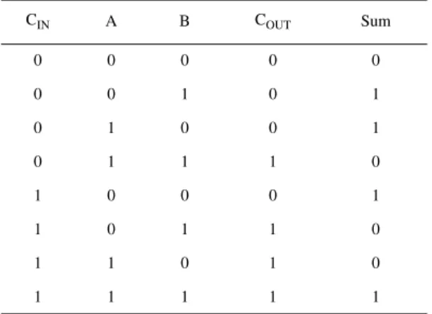
This logic is called a half-adder because it does only part of the job when multiple bits must be added together. Summing multibit data values requires a carry to ripple across the bit positions start-ing from the LSB. The half-adder has no provision for a carry input from the precedstart-ing bit position. A full-adder incorporates a carry input and can therefore be used to implement a complete summa-tion circuit for an arbitrarily large pair of numbers. Table 1.9 lists the complete full-adder input/out-put relationship with a carry ininput/out-put (CIN) from the previous bit position and a carry output (COUT) to the next bit position. Note that all possible sums from zero to three are properly accounted for by combining COUT and sum. When CIN = 0, the circuit behaves exactly like the half-adder.
1 1 1 0 carry bits
1 1 1
+ 0 1 1
1 0 1 0
sum = A⊕B
Digital Logic 15
Full-adder logic can be expressed in a variety of ways. It may be recognized that full-adder logic can be implemented by connecting two half-adders in sequence as shown in Fig. 1.9. This full-adder directly generates a sum by computing the XOR of all three inputs. The carry is obtained by combin-ing the carry from each addition stage. A logical OR is sufficient for COUT, because there can never be a case in which both half-adders generate a carry at the same time. If the A + B half-adder gener-ates a carry, the partial sum will be 0, making a carry from the second half-adder impossible. The as-sociated logic equations are as follows:
Equivalent logic, although in different form, would be obtained using a K-map, because XOR/ XNOR functions are not direct results of K-map AND/OR solutions.
1.6
SUBTRACTION AND NEGATIVE NUMBERS
Binary subtraction is closely related to addition. As with many operations, subtraction can be imple-mented in a variety of ways. It is possible to derive a Boolean equation that directly subtracts two numbers. However, an efficient solution is to add the negative of the subtrahend to the minuend TABLE 1.9 1-Bit Full-Adder Truth Table
CIN A B COUT Sum
0 0 0 0 0
0 0 1 0 1
0 1 0 0 1
0 1 1 1 0
1 0 0 0 1
1 0 1 1 0
1 1 0 1 0
1 1 1 1 1
A B CIN
sum
COUT
FIGURE 1.9 Full-adder logic diagram.
sum = A⊕ ⊕B CIN
16 Digital Fundamentals
rather than directly subtracting the subtrahend from the minuend. These are, of course, identical op-erations: A – B = A + (–B). This type of arithmetic is referred to as subtraction by addition of the
two’s complement. The two’s complement is the negative representation of a number that allows the identity A – B = A + (–B) to hold true.
Subtraction requires a means of expressing negative numbers. To this end, the most-significant bit, or left-most bit, of a binary number is used as the sign-bit when dealing with signed numbers. A negative number is indicated when the sign-bit equals 1. Unsigned arithmetic does not involve a sign-bit, and therefore can express larger absolute numbers, because the MSB is merely an extra digit rather than a sign indicator.
The first step in performing two’s complement subtraction is to convert the subtrahend into a neg-ative equivalent. This conversion is a two-step process. First, the binary number is inverted to yield a
one’s complement. Then, 1 is added to the one’s complement version to yield the desired two’s com-plement number. This is illustrated below:
Observe that the unsigned four-bit number that can represent values from 0 to 1510 now represents
signed values from –8 to 7. The range about zero is asymmetrical because of the sign-bit and the fact that there is no negative 0. Once the two’s complement has been obtained, subtraction is performed by adding the two’s complement subtrahend to the minuend. For example, 7 – 5 = 2 would be per-formed as follows, given the –5 representation obtained above:
Note that the final carry-bit past the sign-bit is ignored. An example of subtraction with a negative result is 3 – 5 = –2.
Here, the result has its sign-bit set, indicating a negative quantity. We can check the answer by calcu-lating the two’s complement of the negative quantity.
0 1 0 1 Original number (5) 1 0 1 0 One’s complement + 0 0 0 1 Add one
1 0 1 1 Two’s complement (–5)
1 1 1 1 0 Carry bits <