Available Online at www.ijpret.com 100
INTERNATIONAL JOURNAL OF PURE AND
APPLIED RESEARCH IN ENGINEERING AND
TECHNOLOGY
A PATH FOR HORIZING YOUR INNOVATIVE WORK
A REVIEW ON HIGH PERFORMANCE OTA TECHNIQUE
PAVAN BHAGAT
Embedded System And Computing, Faculty Of Computer Science Department, G. H. Raisoni College Of Engineering.
Accepted Date: 05/03/2015; Published Date: 01/05/2015
\
Abstract: OTA is very important circuit that is being used today in many devices mostly in communication and data convertors. It also play different role when placed in input and output path. A detailed study of different OTA design techniques is presented here. Study mainly focuses on low voltage and low power techniques for OTAs and presents the comparison of different performance parameters of these techniques. By studying different techniques a design for high linearity and low power have been proposed.
Keywords: OTA Technique, Linearity
Corresponding Author: MR. PAVAN BHAGAT
Access Online On:
www.ijpret.com
How to Cite This Article:
Available Online at www.ijpret.com 101
INTRODUCTION
The operational transconductance amplifier (OTA) forms a very basic functional component in many analog circuits [1], which mainly includes wireless communication system such as CDMA, biomedical circuits and industrial instrumentation and control system[2]. As transconductance of OTA can be adjusted electronically and due to some other factor like high DC Gain and CMRR, it has achieved significant attention as an active device. Where ever used, OTA mainly performs the function of converting input voltage to corresponding output current with maintaining high accuracy and linearity [3]. Not only as operated in current mode, OTA can be operated in voltage mode, and this flexibility allows to use OTA in variety of system design. Due to better dynamic range of differential structure these are more preferred over their single ended counterparts [4].This choice is also made as they have important parameters like better common-mode noise rejection, reduce harmonic distortion, and increased output current swing [5]. At present days, for many sensors networks energy is harvested from environment and also lot of devices are shifted from plug n operate to battery operated, which tremendously motivated researchers for low voltage and low power design techniques. Moreover for low power devices weak inversion mode of operation is preferable. Recently many researchers have proposed work using this technique for OTAs and also different circuit design including delta sigma modulators too [6-12]. Along with it, to improve the transconductance, some researchers also suggest bulk driven MOSFETs to be used. Both the techniques have some complexity related with them, but attempts are being made to minimize these complexities. Along with the earlier application OTAs are good choice for opamps, four-quadrant multipliers, mixers, modulators and continuous time filters. In applications like ADSL and cable modem linearity is the main issue. ADSL and cable modem required linearity over 60dB and video application require minimum linearity of 60dB at 5GHz [2].For better performance, high frequency response and electronic tuning capability Gm-C topology is a good choice for realizing continuous-time filter but it suffers from poor linearity[3], [4].
Figure. 1 Symmetrical OTA Architecture with Enhanced Gm Proposed In [7]
Available Online at www.ijpret.com 102 mainly focus on gate input MOSFETs operated in strong inversion region, very little work consider weak inversion operation and the bulk driven MOSFET. Section II describes the different techniques reviewed. Comparison of these technique is given in section III. Section IV gives Tabular Comparison of results in reviewed papers. Analysis of results is carried out in section V. Section VI gives the conclusion
I.RELATED WORK
For OTA design many designing parameters have been considered by different researchers. This section gives the study of methodology used to improve some common parameters like transconductance, linearity, low power and low voltage design etc.
Figure.2 Topology proposed for fully differntial operational transconductance amplifier in [6]
Available Online at www.ijpret.com 103 transconductance with no change in biasing current. Due to this, circuit is unstable at high operating voltages and biasing current fluctuation will cause the fluctuations in gm. Proposed work in this consumes the power of 221nW with the supply voltage of 0.75V, and achieved CMRR is 103 dB with using 11 transistors. Interesting result of this is less use of transistors which is very low compared to other techniques that will be discussed further in paper.
In [7] Transconductance improvement technique is proposed for bulk driven weak inversion symmetrical OTA design. Technique is based on positive feedback source degeneration. Along with gm improvement an attempt is made to improve dc gain and unity gain frequency without increasing power consumption. For this development of transconductance symmetrical OTA topology is suggested as its output resistance does not depends on differential pair.
Figure. 3 Direct Current Redistribution Technique Proposed In [8]
Figure.1 shows the symmetrical OTA topology with enhanced gm. As shown in Figure. The
enhanced bulk-driven differential pair consists of a current source IB and two matched
transistors Q1 and Q2, in which gates and bulks are split and biased as positive feedback source degeneration. As no new current branch is added in topology it keeps the power consumption same. The basic symmetrical OTA is proposed in [4 of this]. Reported improvement in transconductance is (n+1)/(n-1) as compared to [16]. Results of this are quite interesting as high transconductance of 516.8nS is achieved without increasing the power consumption as no change is made in biasing current of design proposed in [yacha base paper]. As shown in Figure.1 it uses much less transistors typically 11 transistors and still give a good improved frequency response. Circuit operates at 0.4 V and consumes 16.1 nW power which is same as discussed in [yacha base paper] with improvements in dc gain, unity gain frequency, and transconductance the most important, whereas slight degradation in the phase margine is
observed and can be ignored as degradation is very small typically of 200.
Available Online at www.ijpret.com 104 these currents are reallocated with the technique that large current will add to large current and small to small one.With this we get two different currents I1’ and I2’ which will give
difference current 𝐼𝑖𝑑. This difference current is very large compared to 𝐼𝑖𝑑 and thus high
transconductance gain is obtained. This technique is based on gate driven transistors operated in strong inversion mode. Value of Id for strong inversion mode MOSFETS is very high compared to MOSFETS operating in weak inversion mode. Due to high Id devices build with this technique are seen to be consuming higher power and required high voltage. Still a technique called DCRT can be of importance for increasing the transconductance of OTA constructed with the bulk driven MOSFET operating in weak inversion.
Figure.4 Shows the (a) Schematic diagram of underlap DG MOSFET (b) Illustration of source/drain (S/D) doping profile along the channel proposed in [9]
Available Online at www.ijpret.com 105 OTA. Simulation results obtained in this clearly indicate the usability of underlay DG MOSFET for
maintaining the functionality at high temperature by achieving high 𝐴𝑉𝑂−𝑂𝑇𝐴 and 𝐹𝑇−𝑂𝑇𝐴values,
where 𝐴𝑉𝑂−𝑂𝑇𝐴 is the Open loop gain of an OTA and Ft is the Unity gain frequency for an OTA. 3
times higher unity gain frequency is achieved compared to the classical non-overlap S/D design and also when operated at low currents this technique provides 30% improvement in gain (in dB).
In [10] a 0.8uW OTA was introduced that operates in weak inversion region and is bulk driven. Figure.5 illustrates the circuit implementation of source degeneration technique for OTA proposed in [10]. Looking at the power consumption and at first sight it looks little bit high. This OTA is build on 0.35uM technology with operating voltage of 0.8V and considering the process technology, author had got better results. Operating voltages are considerably reduced and a good linearity is also achieved.
Figure.5 Implementation of Source Degeneration Technique Proposed In [10]
Available Online at www.ijpret.com 106 collectively draws current of 1uA from power supply. For the reduction in threshold voltage, input transistors are weakly forward biased to 60mV [10].
II. Comparison of reviewed techniques
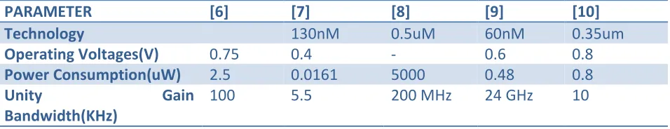
In section II, total 5 different techniques were discussed out of which [8] is gate driven and [6], [7], [9], [10] are bulk driven techniques. All of them concentrates on lowering the operating voltages and power consumption. Drawback of the weak inversion operation with bulk fed technique is that it reduces the input linear range whereas this problem is not considerable in [8] which implements gate driven MOSFETS. As in[6], [7], [9], [10] transistors operate in subthreshold region and thus consumes very low power and also operates at very low power supply typically below 0.8V and maximum power consumption observed in these technique is 0.8uW. On the other hand, DCRT technique which is gate driven consumes the 8mW of power. Comparing the power consumption, it is clear that bulk driven technique operating in weak inversion of subthreshold region offers very less power consumption which is best suited for applications those harvest energy from environment. Looking at the transistor requirement, or we can say requirement of silicon area, all proposed work is nearly same, they require transistors ranging from 8 to 11, but [8] and [9] requires 21 and 17 transistors respectively. [3] is a gate driven technique and due to large number of transistor it consumes power of 5mW which is almost thousand time greater than other techniques still [3] achieves the DC gain of 90 dB which is highest in all techniques and it also provides unity gain bandwidth of 200MHz which is much better than [6],[7],[10] but [9] is exception which provides unity gain bandwidth of 22GHz. Technique proposed in [7] is most promising in terms of transistors used and the power consumption. It typically uses 10 transistors which is least in all the techniques reviewed and consumes the 16 nW of power which is on least side again. This technique uses supply voltage
of 400mV which is least in all techniques. Phase margine provided is 90.80 with unity gain
frequency of 5.5 Khz.
III.TABULAR COMPARISION
Table 1. Comparison Of Different Parameters In Reviewed Techniques
PARAMETER [6] [7] [8] [9] [10]
Technology 130nM 0.5uM 60nM 0.35um
Operating Voltages(V) 0.75 0.4 - 0.6 0.8
Power Consumption(uW) 2.5 0.0161 5000 0.48 0.8
Unity Gain
Bandwidth(KHz)
Available Online at www.ijpret.com 107
Phase Margine(degrees) - 90.8 65 - -
DC Gain(dB) 55 30.61 90 42 -
CMRR(dB) 103 95 85 90
IV. COMPARISION ANALYSIS AND DISCUSSION
Looking at the results in [6], [7], [8], [9] it can be state that results found good for particular application. [7] mainly considers the low power low frequency medical application, [9]considers the redesigning of MOSFETs used so that high performance can be achieved at higher operating voltages, and results obtained are for 500 F and this achieves the unity gain bandwidth of 22GHz with operating voltages of 0.6V. [6] Gives the simple design with high CMRR of 103 dB. [7] Implements DCRT for improving the transconductance. All these work consider specific criteria for improvement where they use basic topology in common. At present era, low voltage and low power is main consideration in most of the application where as it is expected that CMRR, DC Gain, Unity Gain Bandwidth must be as high as possible. A system can be formed that will integrate all the techniques to improve all parameters of OTA and thus an OTA can be designed such that it can be suited for the vast variety of application ranging from low frequency applications like medical application to high frequency like ADSL, ADSM and DSM for wireless communication and Fiber Optic Modems. Whereas High Linearity, DC Gain, CMRR, Unity Gain Bandwidth remain common requirement of all applications.
V.CONCLUSION
Thus, here multiple OTA designing techniques were discussed which uses same basic topology of differential input and some advancement was made to achieve particular goal. Still there is a scope to integrate the techniques and a enhanced OTA can be designed that enjoys the advantages of all the techniques.
ACKNOWLEDGEMENT
Available Online at www.ijpret.com 108
REFERENCES
1. FarzanRezaei, SeyedJavadAzhari, “A Highly Linear Operational Transconductance Amplifier
(OTA) With High Common Mode Rejection Ratio”, 2010 International Conference On Signal Acquisition And Processing, 978-0-7695-3960-7/10 $26.00 © 2010 IEEE
2. Radwene LAAJIMI “A Novel Design Of Low Power And Wide Bandwidth Operational
Transconductance Amplifier Using 0.35μm Technology”,InternationalConfference On Control, Decision And Information Technologies( Codit'13),2013, 978-1-4673-5549-0/13/$31.00 ©2013 IEEE.
3. Luís H. C. Ferreira,TalesCleberPimenta, And Robson L. Moreno, “An Low-Voltage
Ultra-Low-Power CMOS Miller OTA With Rail-To-Rail Input/Output Swing”, IEEE TRANSACTIONS ON CIRCUITS AND SYSTEMS—II: EXPRESS BRIEFS, VOL. 54, NO. 10, OCTOBER 2007
4. Shouri Chatterjee, YannisTsividis, And Peter Kinget, “ 0.5-V Analog Circuit Techniques And
Their Application In OTA And Filter Design”, E, IEEE JOURNAL OF SOLID-STATE CIRCUITS, VOL. 40, NO. 12, DECEMBER 2005
5. Liang Zuo, Syed K. Islam,“ Low-Voltage Bulk-Driven Operational Amplifier With Improved
Transconductance”, IEEE RANSACTIONS ON CIRCUITS AND SYSTEMS—I: REGULAR PAPERS, VOL. 60, NO. 8, AUGUST 2013.
6. ChaiyanChanapromma, KanchanaDaoden, “A CMOS Fully Differential Operational
Transconductance Amplifier Operating In Sub-Threshold Region And Its Application”,2010 2nd International Conference On Signal Processing Systems (ICSPS),
7. Lu´Is H. C. Ferreira, Sameer R. Sonkusale, “GmEnhancement For Bulk-Driven Sub-Threshold
Differential Pair In Nanometer CMOS Process”,Subthreshold Microelectronics Conference (Subvt), 2012 IEEE .
8. Jing Zhu, Yunwu Zhang, Weifeng Sun, Shengli Lu, “A Novel Operational Transconductance
Amplifier With High Gm Using Improved Differential Current Redistribution Technique (DCRT)”, 10th International Conference On ASIC (ASICON), 2013 IEEE
9. AbhinavKranti And G. Alastair Armstrong, “IMPROVING OPERATIONAL
Available Online at www.ijpret.com 109
10.Yodtean A. , Isarasena P. , Thanachayanont A, “O.8 µW CMOS Bulk-Driven Linear
Operational Transconductance Amplifier In O.35 Um Technology”, APCCAS IEEE Conference 2010 .
11.International Technology Roadmap for Semiconductors (Www.Itrs.Net).
12.F. Balestra, S. Cristoloveanu, M. Benachir, J. Birni And T. Elewa, “Double-Gate
Silicon-On-Insulator Transistor With Volume Inversion: A New Device With Greatly Enhanced Performance” IEEE Electron Device Letters, Vol. 8, No. 9,Pp. 410–412, 1987.
13.R. Sarpeshkar, R.F. Lyon, And C. Mead, "A Low-Power Wide-Linearrange Transconductance
Amplifier," Analog Integrated Circuits And Signal Processing, Vol. 13, 1997, Pp. 123-151.
14..M. Carrillo, J.F. Duque-Carrillo, And G. Torelli, "L-V Continuously Tunable CMOS Bulk-Driven
Transconductor For Gm-C Filters," 2008 IEEE International Symposium On Circuits And Systems, 2008, Pp. 896-899.
15.C. Popa And D. Coada, "A New Linearization Technique For A CMOS Differential Amplifier
Using Bulk-Driven Weak Inversion MOS Transistors," 2003 IEEE Int. Symp. In Circuits And Systems, (ISCAS2003),2003, Pp. 589-592.
16.E. D. C. Cotrim And L. H. C. Ferreira, “An Ultra-Power CMOS Symmetrical OTA For
![Figure. 1 Symmetrical OTA Architecture with Enhanced Gm Proposed In [7]](https://thumb-us.123doks.com/thumbv2/123dok_us/8727386.1745565/2.612.186.433.537.614/figure-symmetrical-ota-architecture-enhanced-gm-proposed.webp)
![Figure. 3 Direct Current Redistribution Technique Proposed In [8]](https://thumb-us.123doks.com/thumbv2/123dok_us/8727386.1745565/4.612.185.430.271.358/figure-direct-current-redistribution-technique-proposed.webp)