GENERAL DESCRIPTION
The DS1307 serial real-time clock (RTC) is a low-power, full binary-coded decimal (BCD) clock/calendar plus 56 bytes of NV SRAM. Address and data are transferred serially through an I2C, bidirectional bus. The clock/calendar provides seconds, minutes, hours, day, date, month, and year information. The end of the month date is automatically adjusted for months with fewer than 31 days, including corrections for leap year. The clock operates in either the 24-hour or 12-hour format with AM/PM indicator. The DS1307 has a built-in power-sense circuit that detects power failures and automatically switches to the backup supply. Timekeeping operation continues while the part operates from the backup supply.
TYPICAL OPERATING CIRCUIT
BENEFITS AND FEATURES
Completely Manages All Timekeeping Functions o Real-Time Clock Counts Seconds, Minutes,
Hours, Date of the Month, Month, Day of the Week, and Year with Leap-Year
Compensation Valid Up to 2100
o 56-Byte, Battery-Backed, General-Purpose RAM with Unlimited Writes
o Programmable Square-Wave Output Signal
Simple Serial Port Interfaces to Most Microcontrollers
o I2C Serial Interface
Low Power Operation Extends Battery Backup Run Time
o Consumes Less than 500nA in Battery-Backup Mode with Oscillator Running o Automatic Power-Fail Detect and Switch
Circuitry
8-Pin DIP and 8-Pin SO Minimizes Required Space
Optional Industrial Temperature Range: -40°C to +85°C Supports Operation in a Wide Range of Applications
Underwriters Laboratories® (UL) Recognized
PIN CONFIGURATIONS
VCC SCL SDA X1 X2 VBAT GND SQW/OUT VCC SCL SDA X1 X2 VBAT GND SQW/OUTPDIP (300 mils) SO (150 mils)
TOP VLEW
ORDERING INFORMATION
PART TEMP RANGE VOLTAGE (V) PIN-PACKAGE TOP MARK*
DS1307+ 0°C to +70°C 5.0 8 PDIP (300 mils) DS1307
DS1307N+ -40°C to +85°C 5.0 8 PDIP (300 mils) DS1307N
DS1307Z+ 0°C to +70°C 5.0 8 SO (150 mils) DS1307
DS1307
CPU
V CC
V CC
V CC
SDA SCL
GND X2 X1
V CC R PU RPU
CRYSTAL
SQW/OUT
V BAT
R PU = tr/Cb
DS1307
ABSOLUTE MAXIMUM RATINGS
Voltage Range on Any Pin Relative to Ground ... -0.5V to +7.0V Operating Temperature Range (Noncondensing)
Commercial ... 0°C to +70°C Industrial ... -40°C to +85°C Storage Temperature Range ... -55°C to +125°C Soldering Temperature (DIP, leads) ... +260°C for 10 seconds Soldering Temperature (surface mount)…..……….Refer to the JPC/JEDEC J-STD-020 Specification. Stresses beyond those listed under “Absolute Maximum Ratings” may cause permanent damage to the device. These are stress ratings only, and functional operation of the device at these or any other conditions beyond those indicated in the operational sections of the specifications is not implied. Exposure to the absolute maximum rating conditions for extended periods may affect device reliability.
RECOMMENDED DC OPERATING CONDITIONS
(T
A= 0°C to +70°C, T
A= -40°C to +85°C.) (Notes 1, 2)
PARAMETER SYMBOL CONDITIONS MIN TYP MAX UNITS
Supply Voltage VCC 4.5 5.0 5.5 V
Logic 1 Input VIH 2.2 VCC + 0.3 V
Logic 0 Input VIL -0.3 +0.8 V
VBAT Battery Voltage VBAT 2.0 3 3.5 V
DC ELECTRICAL CHARACTERISTICS
(V
CC= 4.5V to 5.5V; T
A= 0°C to +70°C, T
A= -40°C to +85°C.) (Notes 1, 2)
PARAMETER SYMBOL CONDITIONS MIN TYP MAX UNITS
Input Leakage (SCL) ILI -1 1 µA
I/O Leakage (SDA, SQW/OUT) ILO -1 1 µA
Logic 0 Output (IOL = 5mA) VOL 0.4 V
Active Supply Current (fSCL = 100kHz)
ICCA 1.5 mA
Standby Current ICCS (Note 3) 200 µA
VBAT Leakage Current IBATLKG 5 50 nA
Power-Fail Voltage (VBAT = 3.0V) VPF 1.216 x
VBAT
1.25 x VBAT
1.284 x VBAT
V
DC ELECTRICAL CHARACTERISTICS
(V
CC= 0V, V
BAT= 3.0V; T
A= 0°C to +70°C, T
A= -40°C to +85°C.) (Notes 1, 2)
PARAMETER SYMBOL CONDITIONS MIN TYP MAX UNITS
VBAT Current (OSC ON);
SQW/OUT OFF IBAT1 300 500 nA
VBAT Current (OSC ON);
SQW/OUT ON (32kHz) IBAT2 480 800 nA
VBAT Data-Retention Current
(Oscillator Off) IBATDR 10 100 nA
AC ELECTRICAL CHARACTERISTICS
(V
CC= 4.5V to 5.5V; T
A= 0°C to +70°C, T
A= -40°C to +85°C.)
PARAMETER SYMBOL CONDITIONS MIN TYP MAX UNITS
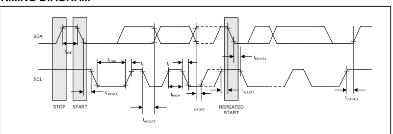
SCL Clock Frequency fSCL 0 100 kHz
Bus Free Time Between a STOP and
START Condition tBUF 4.7 µs
Hold Time (Repeated) START
Condition tHD:STA (Note 4) 4.0 µs
LOW Period of SCL Clock tLOW 4.7 µs
HIGH Period of SCL Clock tHIGH 4.0 µs
Setup Time for a Repeated START
Condition tSU:STA 4.7 µs
Data Hold Time tHD:DAT 0 µs
Data Setup Time tSU:DAT (Notes 5, 6) 250 ns
Rise Time of Both SDA and SCL
Signals tR 1000 ns
Fall Time of Both SDA and SCL
Signals tF 300 ns
Setup Time for STOP Condition tSU:STO 4.7 µs
CAPACITANCE
(T
A= +25°C)
PARAMETER SYMBOL CONDITIONS MIN TYP MAX UNITS
Pin Capacitance (SDA, SCL) CI/O 10 pF
Capacitance Load for Each Bus
Line CB (Note 7) 400 pF
Note 1: All voltages are referenced to ground.
Note 2: Limits at -40°C are guaranteed by design and are not production tested.
Note 3: ICCS specified with VCC = 5.0V and SDA, SCL = 5.0V.
Note 4: After this period, the first clock pulse is generated.
Note 5: A device must internally provide a hold time of at least 300ns for the SDA signal (referred to the VIH(MIN) of the SCL
signal) to bridge the undefined region of the falling edge of SCL.
Note 6: The maximum tHD:DAT only has to be met if the device does not stretch the LOW period (tLOW) of the SCL signal.
TIMING DIAGRAM
Figure 1. Block Diagram
START SDA
STOP SCL
tSU:STO tHD:STA
tSU:STA
REPEATED START tHD:DAT
tHIGH tF tLOW
tR
tHD:STA tBUF
TYPICAL OPERATING CHARACTERISTICS
(VCC = 5.0V, TA = +25°C, unless otherwise noted.)
ICCS vs. VCC
0 10 20 30 40 50 60 70 80 90 100 110 120
1.0 2.0 3.0V 4.0 5.0
CC (V)
SUP PL Y CURRE NT (u A VBAT=3.0V
IBAT vs. Temperature
175.0 225.0 275.0 325.0
-40 -20 0 20 40 60 80 TEMPERATURE (°C) SUP PL Y CURRE NT (n A VCC=0V, VBAT=3.0 SQW=32kHz SQW off
IBAT vs. VBAT
100 150 200 250 300 350 400
2.0 2.5 V 3.0 3.5
BACKUP (V)
SUP PL Y CURRE NT (n A SQW=32kHz SQW off VCC = 0V
SQW/OUT vs. Supply Voltage
32768 32768.1 32768.2 32768.3 32768.4 32768.5
2.0 2.5 3.0 3.5 4.0 4.5 5.0 5.5 Supply (V) FRE QUE NCY (Hz )
PIN DESCRIPTION
PIN NAME FUNCTION
1 X1
Connections for Standard 32.768kHz Quartz Crystal. The internal oscillator circuitry is designed for operation with a crystal having a specified load capacitance (CL) of 12.5pF. X1 is the input to the oscillator and can optionally be connected to an external 32.768kHz oscillator. The output of the internal oscillator, X2, is floated if an external oscillator is connected to X1.
Note: For more information on crystal selection and crystal layout considerations, refer to
Application Note 58: Crystal Considerations with Dallas Real-Time Clocks.
2 X2
3 VBAT
Backup Supply Input for Any Standard 3V Lithium Cell or Other Energy Source. Battery voltage must be held between the minimum and maximum limits for proper operation. Diodes in series between the battery and the VBAT pin may prevent proper operation. If a backup supply is not required, VBAT must be grounded. The nominal power-fail trip point (VPF) voltage at which access to the RTC and user RAM is denied is set by the internal circuitry as 1.25 x VBAT nominal. A lithium battery with 48mAh or greater will back up the DS1307 for more than 10 years in the absence of power at +25°C.
UL recognized to ensure against reverse charging current when used with a lithium battery. Go to: www.maxim-ic.com/qa/info/ul/.
4 GND Ground
5 SDA
Serial Data Input/Output. SDA is the data input/output for the I2C serial interface. The SDA pin is open drain and requires an external pullup resistor. The pullup voltage can be up to 5.5V regardless of the voltage on VCC.
6 SCL
Serial Clock Input. SCL is the clock input for the I2C interface and is used to synchronize data movement on the serial interface. The pullup voltage can be up to 5.5V regardless of the voltage on VCC.
7 SQW/OUT
Square Wave/Output Driver. When enabled, the SQWE bit set to 1, the SQW/OUT pin outputs one of four square-wave frequencies (1Hz, 4kHz, 8kHz, 32kHz). The SQW/OUT pin is open drain and requires an external pullup resistor. SQW/OUT operates with either VCC or VBAT applied. The pullup voltage can be up to 5.5V regardless of the voltage on VCC. If not used, this pin can be left floating.
8 VCC
Primary Power Supply. When voltage is applied within normal limits, the device is fully accessible and data can be written and read. When a backup supply is connected to the device and VCC is below VTP, read and writes are inhibited. However, the timekeeping function continues unaffected by the lower input voltage.
DETAILED DESCRIPTION
The DS1307 is a low-power clock/calendar with 56 bytes of battery-backed SRAM. The clock/calendar provides seconds, minutes, hours, day, date, month, and year information. The date at the end of the month is automatically adjusted for months with fewer than 31 days, including corrections for leap year. The DS1307 operates as a slave device on the I2C bus. Access is obtained by implementing a START condition and providing a device identification code followed by a register address. Subsequent registers can be accessed sequentially until a STOP condition is executed. When VCC falls below 1.25 x VBAT, the device terminates an access in progress and resets the device address counter. Inputs to the device will not be recognized at this time to prevent erroneous data from being written to the device from an out-of-tolerance system. When VCC falls below VBAT, the device switches into a low-current battery-backup mode. Upon power-up, the device switches from battery to VCC when VCC is greater than VBAT +0.2V and recognizes inputs when VCC is greater than 1.25 x VBAT. The block diagram in Figure 1 shows the main elements of the serial RTC.
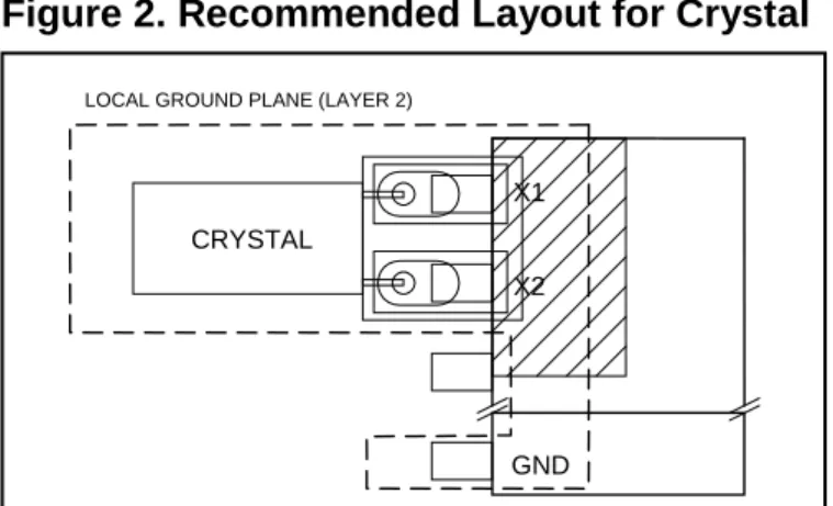
OSCILLATOR CIRCUIT
The DS1307 uses an external 32.768kHz crystal. The oscillator circuit does not require any external resistors or capacitors to operate. Table 1 specifies several crystal parameters for the external crystal. Figure 1 shows a functional schematic of the oscillator circuit. If using a crystal with the specified characteristics, the startup time is usually less than one second.
CLOCK ACCURACY
The accuracy of the clock is dependent upon the accuracy of the crystal and the accuracy of the match between the capacitive load of the oscillator circuit and the capacitive load for which the crystal was trimmed. Additional error will be added by crystal frequency drift caused by temperature shifts. External circuit noise coupled into the oscillator circuit may result in the clock running fast. Refer to Application Note 58: Crystal Considerations with Dallas Real-Time Clocks for detailed information.
Table 1. Crystal Specifications*
PARAMETER SYMBOL MIN TYP MAX UNITS
Nominal Frequency fO 32.768 kHz
Series Resistance ESR 45 kΩ
Load Capacitance CL 12.5 pF
*The crystal, traces, and crystal input pins should be isolated from RF generating signals. Refer to
Application Note 58: Crystal Considerations for Dallas Real-Time Clocks for additional specifications.
Figure 2. Recommended Layout for Crystal
RTC AND RAM ADDRESS MAP
Table 2 shows the address map for the DS1307 RTC and RAM registers. The RTC registers are located in address locations 00h to 07h. The RAM registers are located in address locations 08h to 3Fh. During a multibyte access, when the address pointer reaches 3Fh, the end of RAM space, it wraps around to location 00h, the beginning of the clock space.
NOTE: AVOID ROUTING SIGNAL LINES IN THE CROSSHATCHED AREA (UPPER LEFT QUADRANT) OF THE PACKAGE UNLESS THERE IS A GROUND PLANE BETWEEN THE SIGNAL LINE AND THE DEVICE PACKAGE.
LOCAL GROUND PLANE (LAYER 2)
CRYSTAL
X1
X2
CLOCK AND CALENDAR
The time and calendar information is obtained by reading the appropriate register bytes. Table 2 shows the RTC registers. The time and calendar are set or initialized by writing the appropriate register bytes. The contents of the time and calendar registers are in the BCD format. The day-of-week register increments at midnight. Values that correspond to the day of week are user-defined but must be sequential (i.e., if 1 equals Sunday, then 2 equals Monday, and so on.) Illogical time and date entries result in undefined operation. Bit 7 of Register 0 is the clock halt (CH) bit. When this bit is set to 1, the oscillator is disabled. When cleared to 0, the oscillator is enabled. On first application of power to the device the time and date registers are typically reset to 01/01/00 01 00:00:00 (MM/DD/YY DOW HH:MM:SS). The CH bit in the seconds register will be set to a 1. The clock can be halted whenever the timekeeping functions are not required, which minimizes current (IBATDR).
The DS1307 can be run in either 12-hour or 24-hour mode. Bit 6 of the hours register is defined as the 12-hour or 24-hour mode-select bit. When high, the 12-hour mode is selected. In the 12-hour mode, bit 5 is the AM/PM bit with logic high being PM. In the 24-hour mode, bit 5 is the second 10-hour bit (20 to 23 hours). The hours value must be re-entered whenever the 12/24-hour mode bit is changed.
When reading or writing the time and date registers, secondary (user) buffers are used to prevent errors when the internal registers update. When reading the time and date registers, the user buffers are synchronized to the internal registers on any I2C START. The time information is read from these secondary registers while the clock continues to run. This eliminates the need to re-read the registers in case the internal registers update during a read. The divider chain is reset whenever the seconds register is written. Write transfers occur on the I2C acknowledge from the DS1307. Once the divider chain is reset, to avoid rollover issues, the remaining time and date registers must be written within one second.
Table 2. Timekeeper Registers
ADDRESS BIT 7 BIT 6 BIT 5 BIT 4 BIT 3 BIT 2 BIT 1 BIT 0 FUNCTION RANGE
00h CH 10 Seconds Seconds Seconds 00–59
01h 0 10 Minutes Minutes Minutes 00–59
02h 0
12 10
Hour 10
Hour Hours Hours
1–12 +AM/PM
00–23
24 PM/
AM
03h 0 0 0 0 0 DAY Day 01–07
04h 0 0 10 Date Date Date 01–31
05h 0 0 0 10
Month Month Month 01–12
06h 10 Year Year Year 00–99
07h OUT 0 0 SQWE 0 0 RS1 RS0 Control —
08h–3Fh RAM
56 x 8 00h–FFh
CONTROL REGISTER
The DS1307 control register is used to control the operation of the SQW/OUT pin.
BIT 7 BIT 6 BIT 5 BIT 4 BIT 3 BIT 2 BIT 1 BIT 0
OUT 0 0 SQWE 0 0 RS1 RS0
Bit 7: Output Control (OUT). This bit controls the output level of the SQW/OUT pin when the square-wave output
is disabled. If SQWE = 0, the logic level on the SQW/OUT pin is 1 if OUT = 1 and is 0 if OUT = 0. On initial application of power to the device, this bit is typically set to a 0.
Bit 4: Square-Wave Enable (SQWE). This bit, when set to logic 1, enables the oscillator output. The frequency of
the square-wave output depends upon the value of the RS0 and RS1 bits. With the square-wave output set to 1Hz, the clock registers update on the falling edge of the square wave. On initial application of power to the device, this bit is typically set to a 0.
Bits 1 and 0: Rate Select (RS[1:0]). These bits control the frequency of the wave output when the
square-wave output has been enabled. The following table lists the square-square-wave frequencies that can be selected with the RS bits. On initial application of power to the device, these bits are typically set to a 1.
RS1 RS0 SQW/OUT OUTPUT SQWE OUT
0 0 1Hz 1 X
0 1 4.096kHz 1 X
1 0 8.192kHz 1 X
1 1 32.768kHz 1 X
X X 0 0 0
I
2C DATA BUS
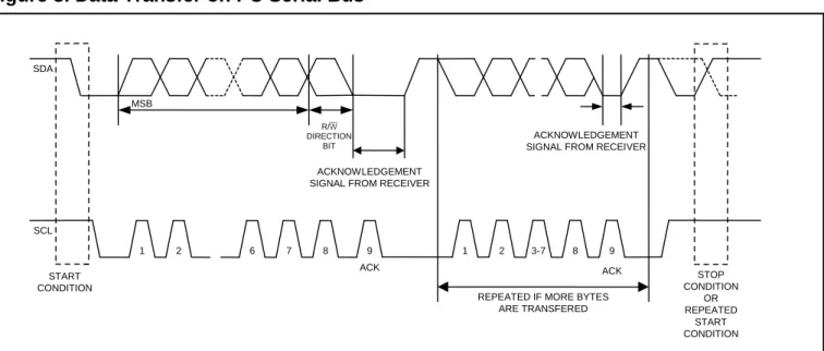
The DS1307 supports the I2C protocol. A device that sends data onto the bus is defined as a transmitter and a device receiving data as a receiver. The device that controls the message is called a master. The devices that are controlled by the master are referred to as slaves. The bus must be controlled by a master device that generates the serial clock (SCL), controls the bus access, and generates the START and STOP conditions. The DS1307 operates as a slave on the I2C bus.
Figures 3, 4, and 5 detail how data is transferred on the I2C bus.
Data transfer can be initiated only when the bus is not busy.
During data transfer, the data line must remain stable whenever the clock line is HIGH. Changes in the data line while the clock line is high will be interpreted as control signals.
Accordingly, the following bus conditions have been defined:
Bus not busy: Both data and clock lines remain HIGH.
START data transfer: A change in the state of the data line, from HIGH to LOW, while the clock is HIGH,
defines a START condition.
STOP data transfer: A change in the state of the data line, from LOW to HIGH, while the clock line is HIGH,
defines the STOP condition.
Data valid: The state of the data line represents valid data when, after a START condition, the data line is
stable for the duration of the HIGH period of the clock signal. The data on the line must be changed during the LOW period of the clock signal. There is one clock pulse per bit of data.
Each data transfer is initiated with a START condition and terminated with a STOP condition. The number of data bytes transferred between START and STOP conditions is not limited, and is determined by the master device. The information is transferred byte-wise and each receiver acknowledges with a ninth bit. Within the I2C bus specifications a standard mode (100kHz clock rate) and a fast mode (400kHz clock rate) are defined. The DS1307 operates in the standard mode (100kHz) only.
Acknowledge: Each receiving device, when addressed, is obliged to generate an acknowledge after the
reception of each byte. The master device must generate an extra clock pulse which is associated with this acknowledge bit.
A device that acknowledges must pull down the SDA line during the acknowledge clock pulse in such a way that the SDA line is stable LOW during the HIGH period of the acknowledge related clock pulse. Of course, setup and hold times must be taken into account. A master must signal an end of data to the slave by not generating an acknowledge bit on the last byte that has been clocked out of the slave. In this case, the slave must leave the data line HIGH to enable the master to generate the STOP condition.
Figure 3. Data Transfer on I
2C Serial Bus
Depending upon the state of the R/W bit, two types of data transfer are possible:
1. Data transfer from a master transmitter to a slave receiver. The first byte transmitted by the master is the
slave address. Next follows a number of data bytes. The slave returns an acknowledge bit after each received byte. Data is transferred with the most significant bit (MSB) first.
2. Data transfer from a slave transmitter to a master receiver. The first byte (the slave address) is transmitted
by the master. The slave then returns an acknowledge bit. This is followed by the slave transmitting a number of data bytes. The master returns an acknowledge bit after all received bytes other than the last byte. At the end of the last received byte, a “not acknowledge” is returned.
The master device generates all the serial clock pulses and the START and STOP conditions. A transfer is ended with a STOP condition or with a repeated START condition. Since a repeated START condition is also the beginning of the next serial transfer, the bus will not be released. Data is transferred with the most significant bit (MSB) first.
ACKNOWLEDGEMENT SIGNAL FROM RECEIVER
ACKNOWLEDGEMENT SIGNAL FROM RECEIVER
R/ W DIRECTION
BIT
REPEATED IF MORE BYTES ARE TRANSFERED START
CONDITION
STOP CONDITION
OR REPEATED
START CONDITION MSB
1 2 6 7 8 9 1 2 3-7 8 9
ACK ACK
SDA
... A
XXXXXXXX A
1101000
S 0 XXXXXXXX A XXXXXXXX A XXXXXXXX A P
<Slave Address> <Word Address (n)> <Data(n)> <Data(n+1)> <Data(n+X)>
S - Start
A - Acknowledge (ACK) P - Stop
<R
W
>
DATA TRANSFERRED (X+1 BYTES + ACKNOWLEDGE) Master to slave
Slave to master
A XXXXXXXX A
1101000
S 1 XXXXXXXX A XXXXXXXX XXXXXXXX A P
<Slave Address> <Data(n)> <Data(n+1)> <Data(n+2)> <Data(n+X)>
S - Start
A - Acknowledge (ACK) P - Stop
A - Not Acknowledge (NACK)
<R
W
>
DATA TRANSFERRED
(X+1 BYTES + ACKNOWLEDGE); NOTE: LAST DATA BYTE IS FOLLOWED BY A NOT ACKNOWLEDGE (A) SIGNAL) Master to slave
Slave to master
... A
The DS1307 can operate in the following two modes:
1. Slave Receiver Mode (Write Mode): Serial data and clock are received through SDA and SCL. After
each byte is received an acknowledge bit is transmitted. START and STOP conditions are recognized as the beginning and end of a serial transfer. Hardware performs address recognition after reception of the slave address and direction bit (see Figure 4). The slave address byte is the first byte received after the master generates the START condition. The slave address byte contains the 7-bit DS1307 address, which is 1101000, followed by the direction bit (R/W), which for a write is 0. After receiving and decoding the slave address byte, the DS1307 outputs an acknowledge on SDA. After the DS1307 acknowledges the slave address + write bit, the master transmits a word address to the DS1307. This sets the register pointer on the DS1307, with the DS1307 acknowledging the transfer. The master can then transmit zero or more bytes of data with the DS1307 acknowledging each byte received. The register pointer automatically increments after each data byte are written. The master will generate a STOP condition to terminate the data write.
2. Slave Transmitter Mode (Read Mode): The first byte is received and handled as in the slave receiver
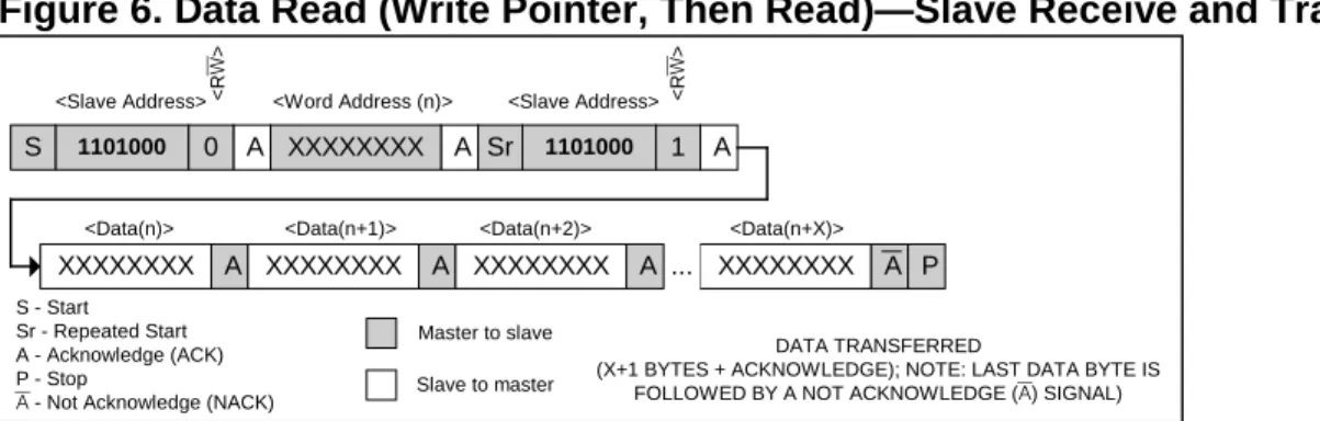
mode. However, in this mode, the direction bit will indicate that the transfer direction is reversed. The DS1307 transmits serial data on SDA while the serial clock is input on SCL. START and STOP conditions are recognized as the beginning and end of a serial transfer (see Figure 5). The slave address byte is the first byte received after the START condition is generated by the master. The slave address byte contains the 7-bit DS1307 address, which is 1101000, followed by the direction bit (R/W), which is 1 for a read. After receiving and decoding the slave address the DS1307 outputs an acknowledge on SDA. The DS1307 then begins to transmit data starting with the register address pointed to by the register pointer. If the register pointer is not written to before the initiation of a read mode the first address that is read is the last one stored in the register pointer. The register pointer automatically increments after each byte are read. The DS1307 must receive a Not Acknowledge to end a read.
Figure 4. Data Write—Slave Receiver Mode
A XXXXXXXX
1101000
S
XXXXXXXX A XXXXXXXX XXXXXXXX A P
<Slave Address> <Word Address (n)> <Slave Address>
S - Start Sr - Repeated Start A - Acknowledge (ACK) P - Stop
A - Not Acknowledge (NACK)
<R
W
>
DATA TRANSFERRED
(X+1 BYTES + ACKNOWLEDGE); NOTE: LAST DATA BYTE IS FOLLOWED BY A NOT ACKNOWLEDGE (A) SIGNAL) Master to slave
Slave to master
... A
XXXXXXXX A
0 Sr 1101000 1 A
<Data(n)> <Data(n+1)> <Data(n+2)> <Data(n+X)>
<R
W
>
A
Figure 6. Data Read (Write Pointer, Then Read)—Slave Receive and Transmit
PACKAGE INFORMATION
For the latest package outline information and land patterns, go to www.maxim-ic.com/packages.
PACKAGE TYPE PACKAGE CODE DOCUMENT NO.
8 PDIP — 21-0043
REVISION HISTORY
REVISIONDATE DESCRIPTION
PAGES CHANGED
100208
Moved the Typical Operating Circuit and Pin Configurations to first page. 1
Removed the leaded part numbers from the Ordering Information table. 1
Added an open-drain transistor to SQW/OUT in the block diagram (Figure 1). 4 Added the pullup voltage range for SDA, SCL, and SQW/OUT to the Pin
Description table and noted that SQW/OUT can be left open if not used. 6
Added default time and date values on first application of power to the Clock and Calendar section and deleted the note that initial power-on state is not defined.
8 Added default on initial application of power to bit info in the Control Register
section. 9
Updated the Package Information section to reflect new package outline
drawing numbers. 13