A High Speed 16*16 Multiplier Based On Urdhva Tiryakbhyam Sutra
B.Ratna Raju
D.V.Satish
Kakinada Institute Of Engineering & Technology
Kakinada Institute Of Engineering & Technology
[email protected]
[email protected]
Abstract
It is an ancient methodology of Indian mathematics as it contains a 16 SUTRAS (formulae). A high speed complex 16 *16 multiplier design by using urdhva tiryakbhyam sutra is presented in this paper. By using this sutra the partial products and sums are generated in one step which reduces the design of architecture in processor’s. By using this sutra we can reduce the time with high extent when compare to array and booth multiplier. It can be implemented in many Digital Signal Processing (DSP) applications such as convolution, Fast
Fourier Transform(FFT) filtering and in
microprocessors. By using this method we reduce the propagation delay in comparison with array based architecture and parallel adder based implementation which are most commonly used architectures .The main parameters of this paper is propagation delay and dynamic power consumption were calculated and found reduced.
Key Words- booth multiplier, FFT, DSP, propagation delay.
I. Introduction
Multiplication is an fundamental function in arithmetic operations based on this operations such as Multiply and Accumulate(MAC) and inner product are among some of the frequently used
Computation-Intensive Arithmetic Functions(CIAF) currently
implemented in many Digital Signal Processing(DSP) applications such as convolution, Fast Fourier Transform(FFT), filtering and in microprocessors in its arithmetic and logic unit. Since multiplication dominates the execution time of most DSP algorithms, so there is a need of high speed multiplier. Currently, multiplication time is still the dominant factor in determining the instruction cycle time of a DSP chip. The demand for high speed processing has been increasing as a result of expanding computer and signal processing applications.
Higher throughput arithmetic operations are important to achieve the desired performance in many real-time signal and image processing applications. One of the key arithmetic operations in such applications is multiplication and the development of fast multiplier circuit has been a subject of interest over decades. Reducing the time delay and power consumption are very essential requirements for many applications. This work presents different multiplier architectures.
In this paper a simple 16 bit digital multiplier is proposed which is based on Urdhva Tiryakbhyam (Vertically & Crosswise) Sutra of the Vedic Math’s. Two binary numbers (16-bit each) are multiplied with this Sutra. The main concept of this paper is that the power consumption of the circuit & propagation delay of the proposed architecture.
Array multiplier, Booth Multiplier are some of the standard approaches used in implementation of binary multiplier which are suitable for VLSI implementation The paper is organized as follows. Section II describes the booth multiplier III describes the basic methodology of Vedic multiplication technique. Section IV describes the proposed multiplier architecture based on Vedic multiplication and the generalized algorithm for N x N bit Vedic multiplier. Section V describes the design and implementation of Vedic multiplier module by using XilinxISE12.1. Section VI comprises of Result and Discussion in which device utilization summary and computational path delay obtained for the proposed Vedic multiplier (after synthesis) is discussed. Finally Section VII comprises of Conclusion.
II. Booth Multiplier
array to control the operations performed by the adder cells. Booth algorithm gives a procedure for multiplying binary integers in signed 2's complement representation on. It operates on the fact that strings of 0's in the multiplier require no addition but just shifting and a string of 1's in the multiplier from bit weight 2k to
weight 2m can be treated as 2K+1-2m. Fig 1 shows the
hardware implementation for Booth's algorithm. It consists of an n-bit adder, control logic and four registers A, B, Q and Q-1. Multiplier and Multiplicand
are loaded into register Q and register B respectively Register A and Q-1are initially set to 0. The n-bit adder
performs addition, inputs of adders comes from multiplicand and content of register A. In case of addition, Add/Sub line is 0, therefore, Cin = 0 and
multiplicand is directly applied as a second input to the n-bit adder. In case of subtraction, Add/sub line is 1, therefore Cin= 1 and multiplicand is complemented and
then applied to the n-bit adder. As a result, the 2’s complement of the multiplicand is added to the contents of register A. The control logic Scans bits Q0 and Q-1
one at a time and generates the control signals to perform the corresponding function. If the two bits are same (1 1 or 0 0), then all the bits of A, Q and Q-1
registers are shifted to right I-bit without addition or subtraction (Add/Subtract Enable = 0). If the two bits differ, then the multiplicand is added to or subtracted from the A register, depending on the status of bits.
Fig.1 Hardware Implementation Of Signed Binary Multiplication For Booth's Algorithm
After addition or subtraction right shift occurs such that the left most bit of A (An–1) is not only shifted into An-2,
but also remains in An-1. This is required to preserve the
sign of the number in A and Q.The flow chart of Booth's algorithm for signed multiplication is shown in Fig 2.
Fig.2 Flow Chart Of Booth's Algorithm For Signed Multiplication
Example-1 0101(5) x 0100(4)
Form the above example it can be proved that the addition/subtraction operation can be skipped if the successive bits in the multiplicand are same.
Final Product 0101 x 0100 = 00010100
III. Vedic Multiplication Technique
The use of Vedic mathematics is to reduces the typical calculations in conventional mathematics to very simple one. Because the Vedic formulae are claimed to be based on the natural principles on which the human mind works. Vedic Mathematics is a methodology of arithmetic rules that allow more efficient speed implementation. It also provides some effective algorithms which can be applied to various branches of engineering such as computing.
A. Urdhva Tiryakbhyam Sutra
work, we apply the same ideas to the binary number system to make the proposed algorithm compatible with the digital hardware. It is a general multiplication formula applicable to all cases of multiplication. It literally means “Vertically and Crosswise”.
It is based on a novel concept through which the generation of all partial products can be done with the concurrent addition of these partial products. The algorithm can be generalized for n x n bit number. Since the partial products and their sums are calculated in parallel and the multiplier is independent of the clock frequency of the processor. Due to its regular structure, it can be easily layout in microprocessors and designers can easily circumvent these problems to avoid catastrophic device failures. The processing power of multiplier can easily be increased by increasing the input and output data bus widths since it has a quite a regular structure. Due to its regular structure, it can be easily layout in a silicon chip. The Multiplier based on this sutra has the advantage that as the number of bits increases, gate delay and area increases very slowly as compared to other conventional multipliers.
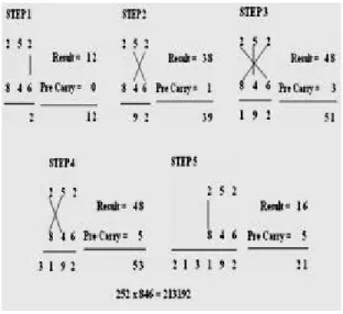
B. Multiplication of two decimal numbers 252 x 846
To illustrate this scheme, let us consider the multiplication of two decimal numbers 252 x 846 by Urdhva-Tiryakbhyam method as shown in Fig. 3. The digits on the both sides of the line are multiplied and added with the carry from the previous step. This generates one of the bits of the result and a carry. This carry is added in the next step and hence the process goes on. If more than one line are there in one step, all the results are added to the previous carry. In each step, least significant bit acts as the result bit and all other bits act as carry for the next step. Initially the carry is taken to be zero.
Fig. 3. Multiplication Of Two Decimal Numbers 252 *846
IV. The Proposed Multiplier Architecture
The hardware architecture of 2X2, 4x4 and 8x8 bit Vedic multiplier module are displayed in the below sections. Here, “Urdhva-Tiryagbhyam” (Vertically and Crosswise) sutra is used to propose such architecture for the multiplication of two binary numbers. The beauty of Vedic multiplier is that partial product generation and additions are done concurrently. Hence, it is well adapted to parallel processing. The feature makes it more attractive for binary multiplications. This in turn reduces delay, which is the primary motivation behind this work.
A. Vedic Multiplier for 2x2 bit Module
The method is explained below for two, 2 bit numbers
AandBwhereA=a1a0 andB=b1b0 as shown in Fig. 4. Firstly, the least significant bits are multiplied which gives the least significant bit of the final product (vertical). Then, the LSB of the multiplicand is multiplied with the next higher bit of the multiplier and added with, the product of LSB of multiplier and next higher bit of the multiplicand (crosswise). The sum gives second bit of the final product and the carry is added with the partial product obtained by multiplying the most significant bits to give the sum and carry. The sum is the third corresponding bit and carry becomes the fourth bit of the final product
s0 =a0b0; (1)
c1s1 =a1b0 +a0b1; (2)
c2s2 =c1 +a1b1; (3)
The final result will be c2s2s1s0. This multiplication method is applicable for all the cases.
Fig.4 The Vedic Multiplication Method For Two 2 Bit Binary Numbers
conventional Array Multiplier .Hence it is concluded that multiplication of 2 bit binary numbers by Vedic method does not made significant effect in improvement of the multiplier’s efficiency.
Very precisely we can state that the total delay is only 2-half adder delays, after final bit products are generated, which is very similar to Array multiplier. So we switch over to the implementation of 4x4 bit Vedic multiplier which uses the 2x2 bit multiplier as a basic building block. The same method can be extended for input bits 4 & 8. But for higher no. of bits in input, little modification is required.
Fig.5. Block Diagram Of 2x2 Bit Vedic Multiplier
B. Vedic Multiplier for 4x4 bit Module
The 4x4 bit Vedic multiplier module is implemented using four 2x2 bit Vedic multiplier modules as discussed in Fig. 6.
Let’s analyze 4x4 multiplications, say A= A3 A2A1A0
and B= B3 B2 B1 B0. The output line for the
multiplication result is – S7 S6S5S4 S3 S2 S1 S0 .Let’s
divide A and B into two parts, say A3A2& A1A0for A
and B3 B2 & B1B0 for B. Using the fundamental of
Vedic multiplication, taking two bit at a time and using 2 bit multiplier block, we can have the following structure for multiplication as shown in Fig. 7.
Fig.6 Sample Presentation For 4x4 Bit Vedic Multiplication
Each block as shown above is 2x2 bit Vedic multiplier. First 2x2 bit multiplier inputs are A1A0 and B1B0. The last block is 2x2 bit multiplier with inputs A3 A2 and B3 B2. The middle one shows two 2x2 bit multiplier with inputs A3 A2 & B1B0 and A1A0 & B3 B2. So the final result of multiplication, which is of 8 bit, S7 S6S5S4 S3 S2 S1 S0. To understand the concept, the Block diagram of 4x4 bit Vedic multiplier is shown in Fig. 7. To get final product (S7 S6 S5 S4 S3 S2 S1 S0), four 2x2 bit Vedic multiplier (Fig. 3) and three 4-bit Ripple-Carry (RC) Adders are required. The proposed Vedic multiplier can be used to reduce delay. Early literature speaks about Vedic multipliers based on array multiplier structures. On the other hand, we proposed a new architecture, which is efficient in terms of speed. The arrangements of ripple carry Adders shown in Fig. 5, helps us to reduce delay and 8x8 Vedic multiplier modules are implemented easily by using four 4x4 multiplier modules.
Fig7. Block Diagram of 4*4 bit Vedic Multiplier
C. Vedic Multiplier for 8x8 bit Module
The 8x8 bit Vedic multiplier module as shown in the block diagram in Fig. 8 can be easily implemented by using four 4x4 bit Vedic multiplier modules as discussed in the previous section.Let’s analyze 8x8 multiplications, say A= A7 A6 A5 A4A3
A2A1A0and B= B7B6B5B4B3B2B1B0. The output
line for the multiplication result will be of 16 bits as – S15S14S13S12S11S10S9S8S7S6S5S4S3S2S1S0.Let’s
divide A andB into two parts, say the 8 bit multiplicand A can be decomposed into pair of 4 bits AH-AL.
B = (AH-AL) x (BH-BL) = AH x BH + (AH x BL + AL x BH) + AL x BL Using the fundamental of Vedic multiplication, taking four bits at a time and using 4 bit multiplier block as discussed we can perform the multiplication. The outputs of 4x4 bit multipliers are added accordingly to obtain the final product. Here total three 8 bit Ripple-Carry Adders are required as shown in Fig. 8.
Fig. 8 Block Diagram Of 8x8 Bit Vedic Multiplier
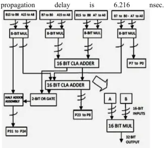
d.Vedic Multiplier for 16x16 bit Module
The design of 16×16 block is a similar arrangement of 8×8 blocks in an optimized manner .The first step in the design of 16×16 block will be grouping the 8 bit (byte) of each 16 bit input. These lower and upper bytes pairs of two inputs will form vertical and crosswise product terms. Each input byte is handled by a separate 8×8 Vedic multiplier to produce sixteen partial product rows. These partial products rows are added in a 16-bit carry look ahead adder optimally to generate final product bits. The schematic of a 16×16 block designed using 8×8 blocks. The partial products represent the Urdhva vertical and cross product [6] terms. Then using or and half adder assembly to find the final product. Power dissipation [7] of this multiplier is 0.18 mW and
propagation delay is 6.216 nsec.
Fig 9 Block Diagram Of 16 X 16 Bit Vedic Multiplier
V. Implementation In Xilinx13.2
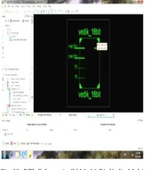
In this work,16x16 bit Vedic multiplier is designed in verilog (Very High Speed Integrated Circuits Hardware Description Language). Logic synthesis and simulation was done in XilinxISE13.2i - Project Navigator and ISim simulator integrated in the Xilinx package. The performance of circuit is evaluated on the Xilinx device family Spartan3, package vq100 and speed grade -4.The RTL schematic of 16x16 bit Vedic multiplier.
“vedic_multi_struct16x16” comprises of four 8x8 bit Vedic multiplier “vedic_multi_struct4x4_1” - vm1, vm2, vm3, vm4 and three 7-bit Ripple Carry Adder “rc_adder_8” - r1, r2, r3 as shown in Fig. 9 while the simulation results obtained are shown in Fig. 11 for verification. In behavioral simulation we have tested for the following input bits:
a) For 16x16 bit Vedic multiplier input, the multiplier x=“1111000011110000” (decimal number system ) and multiplicand y=“0000111100001111” (decimal number
system) and we get 16-bit output
Fig.10. RTL Schematic Of 16x16 Bit Vedic Multiplier
Fig.11. Simulation Result Of 16x16 Bit Vedic Multiplier (Xreg :61680, Yreg:3855, P:237776400)
VI. Results
The synthesis result obtained from proposed Vedic multiplier is faster than Array and Booth multiplier. The device utilization summary of 16x16 bit Vedic multiplier for Xilinx, Spartan family is shown below:
Device Utilization Summary:
Selected Device : 3s50pq208 5
Number of Slices: 448out of 768 58%
Number of 4 input LUTs: 861out of 1536 19%
Number of IOs: 66
Number of bonded IOBs: 66 out of 124 53%
Table 1 shows the comparison of 16x16 bit Conventional multipliers with Vedic multiplier in terms of computational path delay in nanoseconds (ns). The path delay for 16x16 bit Booth multipliers have been taken from S.S. Kerur et al. [11]. The timing result shows that Vedic multiplier has the greatest advantage as compared to other multipliers in terms of execution time.
Table 1 Comparison of 16x16 bit Multipliers (in ns)
s.no Parametersof Comparison
Booth
Multiplier MultiplierVedic
1
Path Delay 9.722ns 6.216ns2
consumptionPower(m Watts) 0.082 0.027
VII. Conclusion
In this paper, we report on a novel complex number multiplier design based on the formulas of the ancient Indian Vedic Mathematics, highly suitable for high speed complex arithmetic circuits which are having wide application in VLSI and signal processing. The implementation was done in HDL and XILINX . This novel architecture combines the advantages of the Vedic mathematics for multiplication which encounters the stages and partial product reduction. The Delay of the proposed Vedic multiplier is 6.216ns and the power consumption is 0.027mW.It is evident from the summary that only 203 logic elements are required for the proposed Architecture. The advantages of this proposed architecture is efficient in speed and area(1ess resources used, such as less number of multipliers and adders) and is Flexible in de design.
References
[1] Prakash Narchi, Siddalingesh S Kerur, Jayashree C Nidagundi, Harish M Kittur and Girish V A. Implementation of Vedic Multiplier for Digital Signal Processing. IJCA Proceedings on International
Conference on VLSI, Communications and
[2] Sumit Vaidya and Deepak Dandekar. “Delay-power perfor-mance comparison of multipliers in VLSI circuit design”. International Journal of Computer Networks & Communications (IJCNC), Vol.2, No.4, July 2010.
[3]H. Thapliyal and H.R Arbania. “A Time-Area-Power Efficient Multiplier and Square Architecture Based On Ancient Indian Vedic Mathematics”, Proceedings of the 2004 International Conference on VLSI (VLSI’04), Las Vegas, Nevada, June 2004, pp. 434-439.
[4]P. D. Chidgupkar and M. T. Karad, “The Implementation of Vedic Algorithms in Digital Signal Processing”, Global J. of Engg. Edu, Vol.8, No.2, 2004, UICEE Published in Australia.
[5]Thapliyal H. and Srinivas M.B, “High Speed Efficient NxN Parallel Hierarchical Overlay Multiplier Architecture Based on Ancient Indian Vedic Mathematics”, Transactions on Engineering, Computing and Technology, 2004, Vol.2.
[6]Harpreet Singh Dhillon and Abhijit Mitra, “A Reduced– Bit Multipliction Algorithm for Digital Arithmetics”, International
Journal of Computational and Mathematical Sciences 2.2 @ www.waset.orgSpring2008.
[7]Honey Durga Tiwari, Ganzorig Gankhuyag, Chan Mo Kim and Yong
Beom Cho, “Multiplier design based on ancient Indian Vedic Mathematician”, International SoC Design Conference, pp. 65- 68, 2008.
[8]Parth Mehta and Dhanashri Gawali, “Conventional versus Vedic mathematics method for Hardware implementation of a multiplier”, International conference on Advances in Computing, Control, and Telecommunication Technologies, pp. 640
[9]Ramalatha, M.Dayalan, K D Dharani, P Priya, and S Deoborah, “High Speed Energy Efficient ALU Design using Vedic Multiplication Techniques”, International Conference on Advances in Computational Tools for Engineering Applications (ACTEA) IEEE, pp. 600-603, July 15-17, 2009.
[10]Sumita Vaidya and Deepak Dandekar, “Delay-Power Performance comparison of Multipliers in VLSI Circuit Design”, International Journal of Computer Networks & Communications (IJCNC), Vol.2, No.4, pp. 47-56, July 2010.