Procedia Computer Science 79 ( 2016 ) 747 – 754
1877-0509 © 2016 The Authors. Published by Elsevier B.V. This is an open access article under the CC BY-NC-ND license (http://creativecommons.org/licenses/by-nc-nd/4.0/).
ScienceDirect
7th International Conference on Communication, Computing and Virtualization 2016
A high performance bulk driven quasi floating gate MOSEFT based
current mirror
Charu Rana
a, Neelofer Afzal
b, Dinesh Prasad
baDeartment of EECE, THE NORTHCAP UNIVERSITY,Gurgaon-122017,India
b ECE Department, Jamia Millia Islamia, New Delhi-110016,India
Abstract
A high performance low voltage bulk driven quasi floating gate MOS based current mirror has been proposed. The combination of bulk driven and quasi FGMOS decreases the input impedance upto 120 Ω which is four times smaller than current mirror based on only bulk driven technique. The bandwidth has also been improved upto 173 MHz which is three folds of bandwidth of conventional bulk driven current mirror. Very high output impedance upto 1GΩ is achieved using self cascode technique in output section depending the value of factor m. Small signal analysis of proposed circuit verifies the simulated results. The circuit is simulated using 0.18μm CMOS technology with supply voltage of ±0.3V. The proposed current mirror is highly suitable for low voltage applications.
© 2016 The Authors. Published by Elsevier B.V.
Peer-review under responsibility of the Organizing Committee of ICCCV 2016.
Keywords: low power; bulk driven ;quasi FGMOS;CMOS;floating gate MOS
1.Introduction
Low voltage low power portable devices have gained enormous significance in the era of miniaturization of analog and mixed signal devices. Current mirror is one of the basic building blocks in CMOS based analog integrated circuits. The main parameters of current mirror on which its performance depends are input and output impedance, current transfer ratio, bandwidth and input and output voltage requirements. The designers of analog integrated circuit must that ensure that a high performance current mirror compatible with scaled technology should be used as a block. Supply voltage has been lowered along with scaling down of geometry of device leading to increased speed and less power consumption [1]. Analog circuits designed using conventional techniques with lowered supply voltage suffers from threshold limitation and performance degradation like signal to noise ratio and dynamic range. © 2016 The Authors. Published by Elsevier B.V. This is an open access article under the CC BY-NC-ND license
(http://creativecommons.org/licenses/by-nc-nd/4.0/).
As a result low voltage analog design techniques are required to design analog and mixed signal circuits for low voltage applications. Researchers are working towards the development low voltage designs to meet the requirements of modern era of scaled technology. Techniques such as bulk driven, sub threshold, gate MOSFET can be used to overcome threshold limitation [2-7]. Unfortunately, low trans conductance is the demerit of these mentioned techniques and hence also suffers from less bandwidth. But it’s quite useful to achieve low supply voltage requirements of the application. Another interesting technique is floating gate MOSFET [2,9-13] . Capacitive voltage divider with high attenuation factors at gate of transistor is implemented in this technique to set dc voltage at floating gate to supply voltage making it suitable for low voltage circuits. Increase in silicon area during fabrication, low transconductance and hence reduced gain bandwidth product is drawback of this technique. It also suffers from charge trapping problem during fabrication. Another technique proposed by Urquidi et. al [14] is quasi floating gate MOSFET which provides solution to this charge trapping by connecting a weak resistor with large value at gate setting a dc voltage to supply rail. Quasi FGMOS can operate for low frequencies and does not lower gain bandwidth product due to large resistor connected. Many circuits have been reported in literature[14-19] using this techniques.
In this paper, combination of bulk driven and quasi FGMOS techniques along with self-cascode structure is used for perusal of high performance of device. Bulk driven method reduces the supply voltage without requiring any extra circuit and quasi FGMOS maintains the gain bandwidth product without lowering it. The only disadvantage is twin well process for fabrication of bulk driven MOS. Self cascode structure is used to provide gain by increasing the output impedance and reducing the miller capacitance effect without requiring high compliance voltage at output. Hence, a self -biased self -cascode bulk driven quasi FGMOS current mirror is proposed in this paper, where the input is applied at bulk terminal of quasi FGMOS transistor and self cascode quasi FGMOS structure in output section for high performance.
Section 2 explains the operation of bulk driven quasi FGMOS transistor followed by self cascode structure. The working of proposed current mirror is explained in Section 3 with simulation results in section 4 followed by conclusion in section 5.
2.Operation of bulk-driven quasi FG technique and self cascode structure
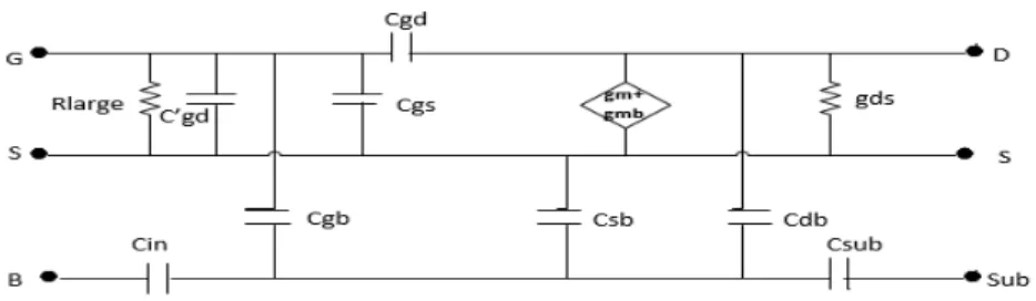
MOSFET is a four terminal device gate denoted as “G”, drain as “D”, source denoted as “S” and bulk “B”. Generally bulk terminal is not being used. Here, Fig. 1 (a) shows the symbol of bulk driven-quasi floating gate MOSFET whereas (b) represents its realization using an active device as large valued resistor. It is important to mention that P well CMOS technology is used for fabrication. Quasi FGMOS structure is utilized to enhance trans conductance and improve gain bandwidth product. As shown in the Fig. 1(b) Input, Vin is connected to the bulk terminal of quasi FGMOS and Vbias is connected an appropriate voltage through resistor “R” which is implemented using MOSFET working in cutoff region. Fig. 2 presents the small signal model of bulk driven quasi FGMOS with no dependency on threshold voltage.
After small signal analysis, transconductance can be given as
ൌሺ୫ା୫ୠሻେଵେ
where C1 is capacitance at input and CT is total capacitance seen at quasi FGMOS transistor and if k= C1/CT then
ൌሺሻ (1)
and transient frequency can approximately be given as
ൌ ୫ୈ୕ୋୗ
ଶሺେୠୱାେୠୱ୳ୠାେୱሻ (2)
Fig. 2 Small signal model of bulk driven QFGMOS transistor
It is seen that bulk driven quasi FGMOS offers better performance than bulk driven MOS and quasi FGMOS. The values of transconductance and transient frequency are larger in this device. For rail to rail operation at low supply voltage, bulk driven quasi FGMOS is a good choice and be exploited in various analog and mixed mode circuits.
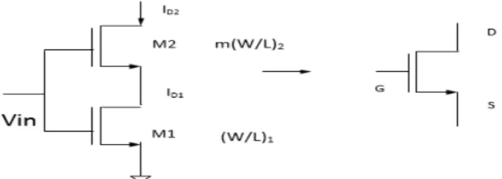
Cascode structures are used to suppress the effect of channel length modulation which is getting quite prominent with the down scaling of technology. It isolate the bottom MOSFET from variations in the output side thus increasing output impedance, rout. Self cascode structure is basically consists of two transistors and can be called as single composite transistor [20-21]. Fig. 3 shows the self cascode structure, both gates of M1 and M2 are driven by single input source along with d c bias voltage. The aspect ratio of M2 is kept larger than of M1 so that M1 is operating in linear region and M2 in saturation leading to high gain. This structure can be represented by a composite transistor as drain to source voltage is quite small of M1 and there is no significant difference between self cascode and single transistor.
The condition is | VTHM2| - |VTHM1| ≥ |VDSsatM2| to give high rout
The effective transconductance and output impedance of a self cascode structure can be given as ൌͳ (3)
ൌʹʹͳǦʹǦͳൎ൫ʹͳǦͳ൯ʹൌ൫ͳͳǦͳ൯ʹൌ൫Ǧͳ൯ʹ (4) where m is ratio of (W/L)2 to (W/L)1
Fig. 3 Self cascode structure
3.Proposed bulk driven quasi FGMOS current mirror
Fig. 4 shows the proposed current mirror utilizing the combination of bulk driven and quasi floating gate metal oxide semiconductor transistors in addition to self cascode technique. The idea is to design high performance block with four bulk driven NMOS transistors where M1 and M3 are quasi floating gate NMOS with the bulk terminal connected to the input. To form quasi FGMOS, capacitors C1 and C2 along with PMOS transistors MP1 and MP2 are used. M3 and M1 are only bulk driven transistors with gate connected to positive supply rail. M1 and M’1 are used to implement self cascode structure as shown in the Fig. 4(a). Self cascode technique used here helps in achieving high output impedance whereas bulk driven quasi FGMOS technique allows the block to operate as low supply voltage with maintained transconductance and wider bandwidth. To simplify the circuit, self cascode structure is replaced by composite transistor M1 with aspect ratio of (W/L)eff as shown in the Fig 4(b) Supply voltage of more than threshold voltage is applied to circuit. Resistor “R” reduces the output voltage required for M1 and M2 to be in saturation. An offset current Ioff is added to I out to nullify the effect of non-linear of MOS transistor which is few μA leading to negligible power dissipation. It is to ensure that VBS should be in reverse biased or little forward bias with less than threshold voltage so that minimum bulk currents flow in the circuit.
Fig. 4(a) Proposed bulkdriven self cascode QFGMOS current mirror (b) Proposed current mirror using composite transistor M2
The effective transconductance of bulk driven quasi FGMOS transistors M1 and M3 shown in Fig. 4(b) can be given as
ͳൌሺͳͳሻ (5)
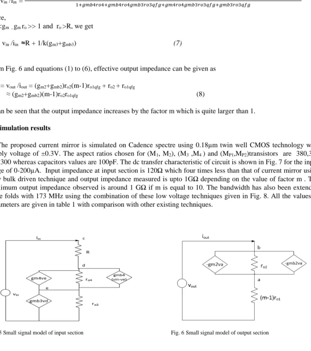
The small signal model of input section of proposed current mirror is shown in Fig 5. The analysis shows that input impedance has been decreased by using combination of bulk driven and quasi FGMOS techniques.
From Fig. 5 and equations (1) to (6), effective input impedance can be given as
rin= vin /iin = ோାସାସଷସାସସଷଷோାସସଷାସସଷଷோାଷାଷଷோ ଵାସସାସସଷଷାସସଷଷାଷଷ Since, gmb<gm , gm ro >> 1 and ro >R, we get rin = vin /iin ≈R + 1/k(gm3+gmb3) (7)
From Fig. 6 and equations (1) to (6), effective output impedance can be given as rout = vout /iout = (gm2+gmb2)ro2(m-1)ro1qfg + ro2 + ro1qfg
≈ (gm2+gmb2)(m-1)ro2ro1qfg (8)
It can be seen that the output impedance increases by the factor m which is quite larger than 1.
4.Simulation results
The proposed current mirror is simulated on Cadence spectre using 0.18μm twin well CMOS technology with supply voltage of ±0.3V. The aspect ratios chosen for (M1, M2), (M3 ,M4 ) and (MP1,MP2)transistors are 380,370 and 300 whereas capacitors values are 100pF. The dc transfer characteristic of circuit is shown in Fig. 7 for the input range of 0-200μA. Input impedance at input section is 120Ω which four times less than that of current mirror using only bulk driven technique and output impedance measured is upto 1GΩ depending on the value of factor m . The maximum output impedance observed is around 1 GΩ if m is equal to 10. The bandwidth has also been extended three folds with 173 MHz using the combination of these low voltage techniques given in Fig. 8. All the values of parameters are given in table 1 with comparison with other existing techniques.
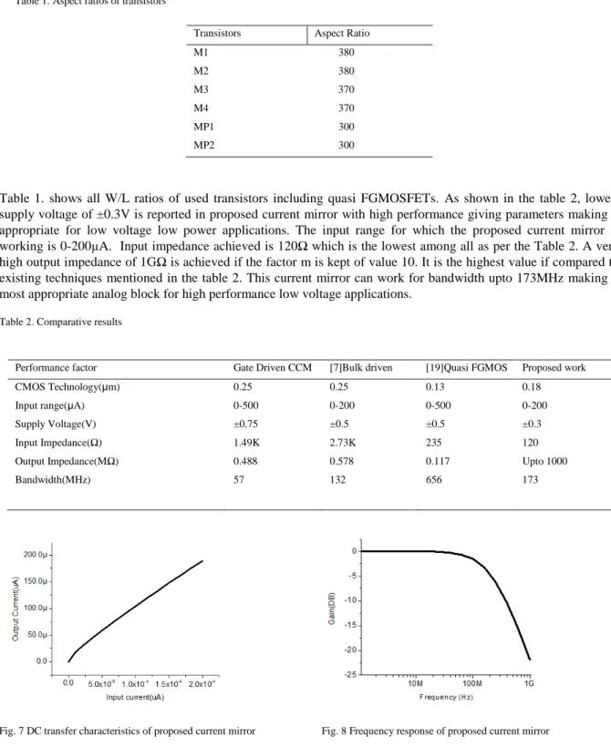
Table 1. Aspect ratios of transistors
Table 1. shows all W/L ratios of used transistors including quasi FGMOSFETs. As shown in the table 2, lowest supply voltage of ±0.3V is reported in proposed current mirror with high performance giving parameters making it appropriate for low voltage low power applications. The input range for which the proposed current mirror is working is 0-200μA. Input impedance achieved is 120Ω which is the lowest among all as per the Table 2. A very high output impedance of 1GΩ is achieved if the factor m is kept of value 10. It is the highest value if compared to existing techniques mentioned in the table 2. This current mirror can work for bandwidth upto 173MHz making it most appropriate analog block for high performance low voltage applications.
Table 2. Comparative results
Performance factor Gate Driven CCM [7]Bulk driven [19]Quasi FGMOS Proposed work
CMOS Technology(μm) 0.25 0.25 0.13 0.18
Input range(μA) 0-500 0-200 0-500 0-200
Supply Voltage(V) ±0.75 ±0.5 ±0.5 ±0.3
Input Impedance(Ω) 1.49K 2.73K 235 120
Output Impedance(MΩ) 0.488 0.578 0.117 Upto 1000
Bandwidth(MHz) 57 132 656 173
Fig. 7 DC transfer characteristics of proposed current mirror Fig. 8 Frequency response of proposed current mirror Transistors Aspect Ratio
M1 380 M2 380 M3 370 M4 370 MP1 300 MP2 300
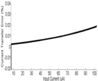
Fig. 9 Current transfer error
The ratio of output current to input current is given in Fig. 9. It can be seen that current transfer ratio is 0.02% which confirms accurate current copy to output.
5.Conclusion
A high performance low voltage bulk driven quasi FGMOSFET based current mirror operating on ±0.3V is proposed in this paper to meet requirements of low voltage applications. A blend of bulk driven, quasi FGMOS and self cascode techniques are used to achieve high performance in terms of supply voltage ,input impedance, output impedance and bandwidth. The circuit is simulated on cadence spectre using CMOS 180nm technology and results are validated by small signal analysis of circuit.
Acknowledgements
Authors thank to ECE department of Jamia Millia Islamia to provide facilities to pursue this work.
References
1. Fayomi, C.J.B., Sawan, M., and Roberts, G.W, Reliable circuit techniques for low-voltage analog design in deep submicron standard CMOS: a tutorial, Analog Integrated Circuits Signal Processing, 2004;39:21–38
2. Khateb, F., Dabbous, S.B.A., and Vlassis, S,A survey of nonconventional techniques for low-voltage low-power analog circuit design’, Radioengineering, 2013;22: 415–427
3. R. He, L. Zhang, Evaluation of modern MOSFET models for bulk-driven applications, 51st Midwest Symposium on Circuits and
Systems. (MWSCA0S);2008: 105–108.
4. Yu-Lung L, We-Bin Y, Ting-Sheng C, Kuo-Hsing C,Designing an ultralow-voltage phase-locked loop using a bulk-driven technique,
IEEE Transaction on Circuit and System -II 2009:339–43.
5. Raikos G, Vlassis S, 0.8 V bulk-driven operational amplifier, Analog Integrated Circuit and Signal Processing ,2010;63:425–32. 6. Raikos G, Vlassis S, Psychalinos C, 0.5 V bulk-driven analog building blocks, AEU International Journal of Electron
Communication ,2012;66:920–7.
7. Aggarwal, B., Gupta, M., and Gupta, A.K.: Analysis of low voltage bulk-driven self-biased high swing cascode current mirror,
Microelectronic Journa., 2013;44:225–235
8. Khateb F, Biolek D,Bulk-driven current differencing transconductance ampli-fier. Circuit System and Signal Processing 2011;30:1071–89.
9. Navarro I, López-Martín AJ, de la Cruz CA, Carlosena A, A compact four-quadrant floating-gate MOS multiplier, Analog Integrated
Circuit and Signal Processing ,2004;41:159–66.
10. Rodriguez-Villegas E, Low power and low voltage circuit design with theFGMOS transistor, IET ,2006.
11. Chawla R, Serrano G, Allen D, Hasler P, Programmable floating-gate second-order sections for Gm-C filter applications, Journal of
13. Babu V.S, Sekhar A, Salini Devi R, Baiju M.R, Floating gate MOSFET based oper-ational transconductance amplifier and study of mismatch, International Journal of Electron Applications ,2009:127–32.
14. C. Urquidi, J. Ramirez Angulo, R.Carjaval and A.Torralba, A new family of low voltage circuits based on quasi floating gate transistors, Proceedings of IEEE Midwest Symposium Circuits and systems , 2002: 93-96.
15. Algueta Miguel JM, De La Cruz Blas CA, Lopez-Martin AJ, CMOS triode transconductor based on quasi-floating-gate transistors.
Electronic Letters ,2010;46:1190–1.
16. Miguel J.M.A, Lopez-Martin A.J, Acosta L, Ramirez-Angulo J, Carvajal R.G,Using floating gate and quasi-floating gate techniques for rail-to-rail tunable CMOS transconductor design, IEEE Transaction on Circuit and Systems, 2011:1604–14.
17. Khateb F, Khatib N, Kubánek D, Low-voltage ultra-low-power current con-veyor based on quasi- floating gate transistors.
Radioengineering ,2012;21:725–35.
18. Lopez-Martin A.J, Acosta L, Algueta J.M, Ramirez-Angulo J, Carvajal R.G, Microp-ower class AB CMOS current conveyor based on quasi-floating gate techniques, 52nd IEEE International Midwest Symposium on Circuits and Systems –MWSCAS’09,2009:140–3. 19. Rockey Gupta, Susheel Sharma , Quasi-floating gate MOSFET based low voltage current mirror, Microelectronics Journal 2012;43
:439–443
20. Comer D.J and Petrie C, The utility of the composite cascade in analog CMOS design, International Journal of Electronics, 2004;91;491-8.
21. Rajput S.S and Jamuar S.S , Low voltage analog circuit design techniques, IEEE circuits systems Magazine , 2002: 24-42.
22. Khateb, F, Bulk-driven floating-gate and bulk-driven quasi-floating gate techniques for low-voltage low-power analog circuits design, AEU-International Journal of Electronic Communication, 2013; 68: 64–1.
23. Khateb, F., Jaikl, W., Kumngern, M., and Prommee, P, Comparative study of sub-volt differential difference current conveyors, Microelectronic. Journal, 2013; 44:1278–12.