DEVELOPMENT OF AN AC-DC BUCK POWER FACTOR CORRECTION
MUHAMMAD ISKANDAR BIN IBRAHIM
A PROJECT REPORT SUBMITTED IS PARTIAL FULFILMENT THE REQUIREMENT FOR THE AWARD OF MASTER OF ELECTRICAL ENGINEER
FACULTY OF ELECTRICAL AND ELECTRONICS ENGINEERING UNIVERSITI TUN HUSSIEN ONN MALAYSIA
ABSTRACT
TABLE OF CONTENTS
CHAPTER ITEM PAGE
Title I
Declaration II
Acknowledgment III
Abstract IV
Table of Contents V
List of Figure VII
CHAPTER 1 INTRODUCTION 1
1.1 Project Background 1
1.2 Problem Statements 3
1.3 Project Objectives 3
1.4 Project Scopes 3
CHAPTER 2 LITERATURE REVIEW 4
2.1 Theories 4
2.2 Description of Previous Methods 4
2.3 Introduction to Buck converter 6
2.3.1 Circuit description 6
2.3.2 Circuit Operation 6
CHAPTER 3 METHODOLOGY 9
3.1 Introduction 9
3.1.1 Identify Design Requirement 10
3.1.1.1 Theory of Power Factor 10
3.1.1.2 Theory of Rectifier 11
3.2 PID control design 12
3.2.1 Derivative Term 13
3.2.2 Integral Term 14
3.2.3 Proportional Term 15
3.3. Saw-Tooth Signal Generator 16
3.4 Buck converter formula 17
CHAPTER 4 SIMULATION MODEL 18
4.1 Simulation Close Loop Result 18
4.1.1 Changes of Output Load 23
4.1.2 Hardware Close loop Result 32
4.1.3 Sawtooth Waveform 32
4.1.4 IGBT Waveform 33
4.1.5 Analysis of PID controller 34
4.2 Simulation Open Loop Result 36
4.2.1 Changes of Output Load 39
4.2.2 Hardware Open loop Result 44
4.2.3 Analysis of Input current 45
CHAPTER 5 Conclusion and discussion 48
5.1 Conclusion 48
5.2 Recommendation 48
LIST OF FIGURE
No. Title Page
Figure 1 Input voltage from full-bridge rectifier and typical drive that can drive Buck-Boost
4
Figure 2 Buck, Boost and Buck-Boost basic system and waveform 5
Figure 3 Buck converter during switch ON and OFF 7
Figure 4 Project Plan 9
Figure 5 Ratio between P(Real), Q(Reactive) and S(Apparent) 10
Figure 6 Voltage, Current and Power Factor 11
Figure 7 Simple rectifier without power factor correction (PFC) draws current from the AC mains with a high harmonic content, and hence a low power factor
12
Figure 8 Plot of PV vs time, for three values of Kd (Kp and Ki held constant) 13 Figure 9 Plot of PV vs time, for three values of Ki (Kp and Kd held constant) 14 Figure 10 Plot of PV vs time, for three values of Kp (Ki and Kd held constant) 15
Figure 11 Saw-tooth waveform generator 16
Figure 12 AC-DC by using Step-down transformer and rectifier 18 Figure 13 AC-DC by using rectifier and Buck PFC circuit 18 Figure 14 Rectifier input current and voltage of AC-DC by using Step-down
transformer and rectifier
19
Figure 15 Buck input current and voltage of AC-DC by using rectifier and Buck PFC circuit
19
Figure 16 Rectifier, Active and Reactive Power of AC-DC by using Step-down transformer and rectifier
20
Figure 17 Buck Active and Reactive Power of AC-DC by using rectifier and Buck PFC circuit
20
Figure 18 Rectifier THD and power factor of AC-DC by using Step-down transformer and rectifier
21
Figure 19 Buck THD and power factor of AC-DC by using rectifier and Buck PFC circuit
21
Figure 20 Rectifier Output Voltage of AC-DC by using Step-down transformer and rectifier
Figure 21 Buck Output Voltage of AC-DC by using rectifier and Buck PFC circuit
22
Figure 22 Output load 10,000ohm for Output Voltage of AC-DC by using rectifier and Buck PFC circuit
23
Figure 23 Output load 1,000ohm for Output Voltage of AC-DC by using rectifier and Buck PFC circuit
23
Figure 24 Output load 100ohm for Output Voltage of AC-DC by using rectifier and Buck PFC circuit
24
Figure 25 Output load 10ohm for Output Voltage of AC-DC by using rectifier and Buck PFC circuit
24
Figure 26 Output load 10,000ohm for Power Factor of AC-DC by using rectifier and Buck PFC circuit
25
Figure 27 Output load 1,000ohm for Power Factor of AC-DC by using rectifier and Buck PFC circuit
25
Figure 28 Output load 100ohm for Output Factor of AC-DC by using rectifier and Buck PFC circuit
26
Figure 29 Output load 10ohm for Power Factor of AC-DC by using rectifier and Buck PFC circuit
26
Figure 30 Output load 10,000ohm for Input Current &Voltage of AC-DC by using rectifier and Buck PFC circuit
27
Figure 31 Output load 1,000ohm for Input Current &Voltage of AC-DC by using rectifier and Buck PFC circuit
27
Figure 32 Output load 100ohm for Input Current &Voltage of AC-DC by using rectifier and Buck PFC circuit
28
Figure 33 Output load 10ohm for Input Current &Voltage of AC-DC by using rectifier and Buck PFC circuit
28
Figure 34 Output load 10ohm, 0.1H for Output Voltage of AC-DC by using rectifier and Buck PFC circuit
29
Figure 35 Output load 10ohm, 1H for Output Voltage of AC-DC by using rectifier and Buck PFC circuit
29
Figure 36 Output load 10ohm, 0.1H for Input Current & Voltage of AC-DC by using rectifier and Buck PFC circuit
30
by using rectifier and Buck PFC circuit
Figure 38 Output load 10ohm, 0.1H for Power Factor of AC-DC by using rectifier and Buck PFC circuit
31
Figure 39 Output load 10ohm, 1H for Input Current & Voltage of AC-DC by using rectifier and Buck PFC circuit
31
Figure 40 With Buck Converter 32
Figure 41 Without Buck-Converter 32
Figure 42 Hardware waveform for sawtooth & PWM 33
Figure 43 Hardware waveform for IGBT-Gate current & PWM 34
Figure 44 AC-DC Using Rectifier by Close Loop Feedback 35
Figure 45 Hardware waveform for Input Current & Voltage 35
Figure 46 Simulation model for Buck PFC open loop 36
Figure 47 Power factor simulation result for Buck PFC open loop 37 Figure 48 Active and reactive simulation result for Buck PFC open loop 38 Figure 49 Output load 1ohm for Output Voltage of AC-DC by using
rectifier and Buck PFC circuit (Open Loop)
39
Figure 50 Output load 10ohm, 10H for Output Voltage of AC-DC by using rectifier and Buck PFC circuit (Open Loop)
40
Figure 51 Output load 100ohm for Output Voltage of AC-DC by using rectifier and Buck PFC circuit (Open Loop)
40
Figure 52 Output load 1ohm for Input Voltage & Current of AC-DC by using rectifier and Buck PFC circuit (Open Loop)
41
Figure 53 Output load 10ohm, 10H for Input Voltage & Current of AC-DC by using rectifier and Buck PFC circuit (Open Loop)
42
Figure 54 Output load 100ohm for Input Voltage & Current of AC-DC by using rectifier and Buck PFC circuit (Open Loop)
42
Figure 55 Output load 1ohm for Power Factor of AC-DC by using rectifier and Buck PFC circuit (Open Loop)
43
Figure 56 Output load 10ohm, 10H for Power Factor of AC-DC by using rectifier and Buck PFC circuit (Open Loop)
43
Figure 57 Output load 100ohm for Power Factor of AC-DC by using rectifier and Buck PFC circuit (Open Loop)
43
CHAPTER 1
INTRODUCTION
1.1Project Background
Power factor can be defined as:-
The ratio of active or real power to the apparent power.
If the load is purely resistive, then the real power will be same as Vrms x Irms
factor will be 1.0. And if the load is not purely resistive, the power factor will be
below 1.0. Hence, the PFC are developed especially for non-linear load so that the
power factor is improved which means it tries to make the input current in response to
the input voltage, so that a constant ratio is maintained between the voltage and
current. This would ensure the input to be resistive in nature and thus, the power
Nearly all single-phase AC-to-DC power supplies have a full-wave bridge
rectifier circuit on the input, which attempts to hold its DC voltage constant between
the half-cycle peaks of the input voltage sine wave. The capacitor charging current
only flows when the input voltage (less the voltage drops across the rectifiers) is
greater than the voltage on the capacitor; when it is less, the rectifiers are off and little
or no current flows. Therefore, the current is highly non-sinusoidal. Uncorrected
power factors may be as low as 0.5 or 0.6 for this type of rectifier design. Hence,
various measures are taken to improve the power factor of a system.
Some study describes the use and design of a Buck Converter and Boost
pre-regulator for the Power Factor Correction[1], [2]. Then compares various DC-DC
Converter topologies for Power Factor Correction [3].
Power Factor Correction circuit is to make the line current follow the
waveform of the line voltage. It will make the load behaves like a purely resistor and
hence to improve the power factor. Our project work makes the use of Buck
Converter in the Power Factor Correction circuit so as to improve the power factor.
We started our project by study and analysis of power factor of a system. Then
make simulations on MATLAB simulation software using full wave rectifier. After
studying and analyzing the input current and voltage waveforms, we introduced a
Buck Converter in the circuit and then analyzed its effect in improving the power
1.2Problem Statements
Power factor in non-linear load such as rectifier distort the current from the
system. Power factor can be increase by passive or active power factor. This system
can change waveform drawn by load to linear load. The purpose of this project is to
improve power factor on AC to DC rectifier circuit.
1.3Project Objectives
This project has been developed to enhance the achievement in the following matter:-
a) To implement simulation of PFC of Buck Converter using software MATLAB
simulink.
b) To construct hardware of PFC of Buck Converter.
1.4Project Scopes
The scope of this project is segregate with software development and hardware
development:
a) Simulation converter using MATLAB simulink software
b) Testing the converter to compute the result same as simulation and can achieve
CHAPTER 2
LITERATURE REVIEW
2.1Theories
In this chapter, three of the most common topologies of PFC implement.
Advantages and disadvantages for each of them will highlight. The common
topologies are buck, boost and buck boost.
2.2Description of Previous Methods
Starting with the Buck converter, the output voltage provided to the load is
always less then the input terminal which also know as step-down converter. For the
implementation of PFC, buck converter will function in discontinue condition due to
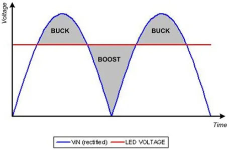
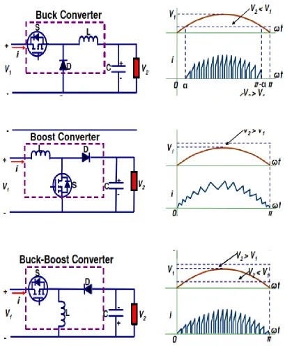
[image:12.595.186.414.572.722.2]AC signal.
Figure 1: Input voltage from full-bridge rectifier and typical drive that can drive
The Boost converter has the output voltage greater then the input which
known as step-up converter. When using this topology, the PFC the current is
continue. As shown in the current diagram, CCM (Continue Conduction Mode)
allows a continues current through the inductor.
The combination of the Buck Boost converter, as the name suggests, is a
combination of a buck converter and a boost converter, so that the characteristic of
[image:13.595.97.506.233.729.2]both are achievable. The output voltage can be greater of lower that the input voltage.
One disadvantage of the buck and buck-boost topology is that the switch is not
refer to ground, which makes the driver circuitry complex. The buck-boost topology
also inverts the sign of the output voltage, which bring another disadvantage when
comes to a cost.
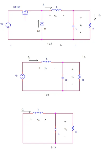
2.3: Introduction to Buck converter
2.3.1 Circuit description. The three basic dc-dc converters use a pair of switches,
usually one controlled (MOSFET) and one uncontrolled (diode), to achieve
unidirectional power flow from input to output. The converters also use one capacitor
and one inductor to store and transfer energy from input to output. They also filter or
smooth voltage and current.
The dc-dc converters can have two distinct modes of operation: Continuous
conduction mode (CCM) and discontinuous conduction mode (DCM). In practice, a
converter may operate in both modes, which have significantly different
characteristics. Therefore, a converter and its control should be designed based on
both modes of operation. However, for this course we only consider the dc-dc
converters operated in CCM.
2.3.2 Circuit Operation. When the switch is on for a time duration DT, the switch
conducts the inductor current and the diode becomes reverse biased. This results in a
positive voltage v =Vg – Vo across the inductor. This voltage causes a linear increase
in the inductor current i. When the switch is turned off, because of the inductive
energy storage, i continue to flow.
This current now flows through the diode, and vL = -VoL for a time duration (1-D)T
2.3Introduction of PID controller
The PID controller is the most common form of feedback. It was an essential element
of early governors and it became the standard tool when process control emerged in
the 1940s. In process control today, more than 95% of the control loops are of PID
type, most loops are actually PI control. PID controllers are today found in all areas
where control is used. The controllers come in many different forms. There are
stand-alone systems in boxes for one or a few loops, which are manufactured by the
hundred thousands yearly. PID control is an important ingredient of a distributed
control system. The controllers are also embedded in many special-purpose control
systems. PID control is often combined with logic, sequential functions, selectors, and
simple function blocks to build the complicated automation systems used for energy
production, transportation, and manufacturing. Many sophisticated control strategies,
such as model predictive control, are also organized hierarchically. PID control is
used at the lowest level; the multivariable controller gives the set points to the
controllers at the lower level. It is an important component in every control engineer’s
CHAPTER 3
METHODOLOGY
3.1Introduction
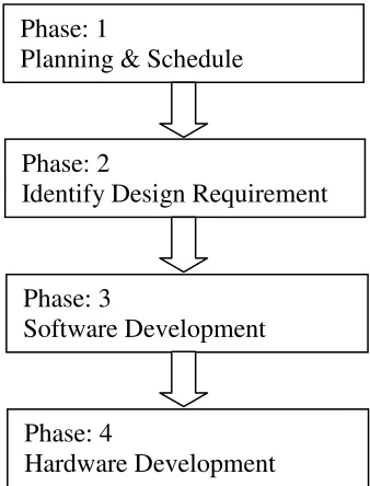
The focus of this cheater is to provide further details of methodology and
approaches to completing this research. This chapter discusses on three main parts,
[image:17.595.200.369.433.655.2]which is PID controller, Sawtooth generator and Buck-converter.
Figure 4: Project Plan Phase: 2
Identify Design Requirement
Phase: 3
Software Development
Phase: 4
Hardware Development Phase: 1
3.1.1 Identify Design Requirement
3.1.1.1 Theory of Power Factor
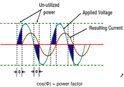
The Power Factor is defined as the ratio between the Real Power and the
Apparent Power in an AC circuit. The Real Power represents the net transferred
energy transferred to the load over one complete AC cycle while the Reactive Power
represents the fraction that is only temporarily stored by the load. The Real Power is
the one measured and monitored for power consumption, and its associated energy
[image:18.595.170.412.265.517.2]being is used to produce mechanical work and heating.
Figure 5: Ratio between P(Real), Q(Reactive) and S(Apparent).
Traditionally, the power factor is associated with the cosine of angle between
the real and apparent power components. For simplicity the apparent power can be
represented as the vector sum of the real and reactive power, but in the case of non
sinusoidal periodical signals a more complex relationship between these components
Figure 6: Voltage, Current and Power Factor
3.1.1.2 Theory of Rectifier
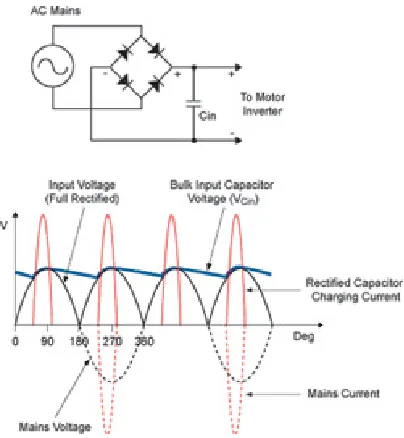
Nearly all single-phase AC-to-DC power supplies have a full-wave bridge
rectifier circuit on the input, followed by a large bulk capacitor, which attempts to
hold its DC voltage constant between the half-cycle peaks of the input voltage sine
wave. Of course, no matter how large it is, the capacitor droops slightly between
half-cycles, so when the next peak comes, the rectifier bridge conducts and recharges the
capacitor.
The capacitor charging current only flows when the input voltage (less the
voltage drops across the rectifiers) is greater than the voltage on the capacitor; when it
is less, the rectifiers are off and little or no current flows. Therefore, the current is
highly non-sinusoidal, as shown in Figure 7. The low power factor caused by the high
harmonic content of the currents causes similar problems for the power company to
those caused by sinusoidal reactive power, only worse. The harmonics cause
distortion in the voltage waveform, and can even cause destructive resonances in the
Uncorrected power factors may be as low as 0,5 or 0,6 for this type of rectifier
design. A similar situation applies to three-phase mains power, but the rectifier bridge
has six diodes instead of four, and the phase peaks six times per cycle instead of
[image:20.595.197.399.152.371.2]twice.
Figure 7: Simple rectifier without power factor correction (PFC) draws current from
the AC mains with a high harmonic content, and hence a low power factor
3.2 PID Control Design
The PID control scheme is named after its three correcting terms, whose sum
constitutes the manipulated variable (MV). The proportional, integral, and derivative
terms are summed to calculate the output of the PID controller. Defining u(t) as the
where
KP: Proportional gain, a tuning parameter
KI: Integral gain, a tuning parameter
KD: Derivative gain, a tuning parameter
e: Error
t: Time or instantaneous time (the present)
T: Variable of integration; takes on values from time 0 to the present .
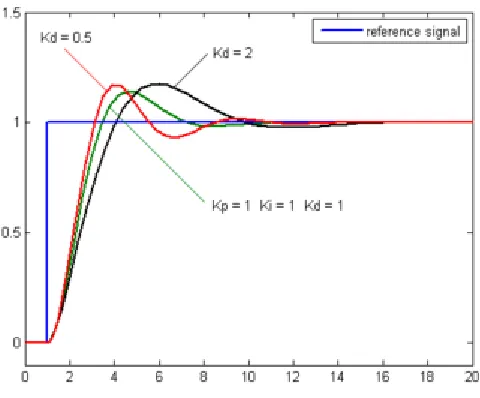
[image:21.595.177.417.377.576.2]3.2.1 Derivative Term
Figure 8: Plot of PV vs time, for three values of Kd (Kp and Ki held constant)
The derivative of the process error is calculated by determining the slope of
the error over time and multiplying this rate of change by the derivative gain KD. The
magnitude of the contribution of the derivative term to the overall control action is
The derivative term is given by:
The derivative term slows the rate of change of the controller output.
Derivative control is used to reduce the magnitude of the overshoot produced by the
integral component and improve the combined controller-process stability. However,
the derivative term slows the transient response of the controller. Also, differentiation
of a signal amplifies noise and thus this term in the controller is highly sensitive to
noise in the error term, and can cause a process to become unstable if the noise and
the derivative gain are sufficiently large. Hence an approximation to a differentiator
with a limited bandwidth is more commonly used. Such a circuit is known as a
phase-lead compensator.
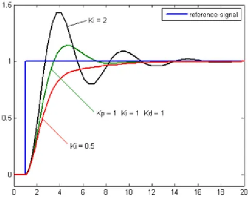
[image:22.595.176.417.429.625.2]3.2.2 Integral Term
Figure 9: Plot of PV vs time, for three values of Ki (Kp and Kd held constant)
The contribution from the integral term is proportional to both the magnitude
of the error and the duration of the error. The integral in a PID controller is the sum of
been corrected previously. The accumulated error is then multiplied by the integral
gain (KI) and added to the controller output.
The integral term is given by:
The integral term accelerates the movement of the process towards setpoint
and eliminates the residual steady-state error that occurs with a pure proportional
controller. However, since the integral term responds to accumulated errors from the
past, it can cause the present value to overshoot the setpoint value (see the section on
loop tuning).
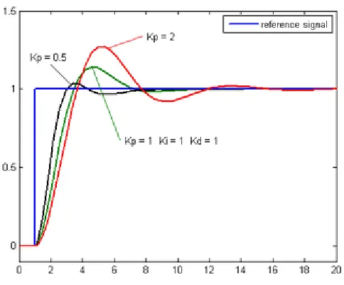
[image:23.595.176.418.452.652.2]3.2.3 Proportional Term
Figure 10: Plot of PV vs time, for three values of Kp (Ki and Kd held constant)
The proportional term produces an output value that is proportional to the
current error value. The proportional response can be adjusted by multiplying the
The proportional term is given by:
A high proportional gain results in a large change in the output for a given
change in the error. If the proportional gain is too high, the system can become
unstable (see the section on loop tuning). In contrast, a small gain results in a small
output response to a large input error, and a less responsive or less sensitive
controller. If the proportional gain is too low, the control action may be too small
when responding to system disturbances. Tuning theory and industrial practice
indicate that the proportional term should contribute the bulk of the output change.
[image:24.595.120.488.431.599.2]3.3 Saw-Tooth Signal Generator
Figure 11: Saw-tooth waveform generator
A saw-tooth waveform generator circuit using a 555 IC is shown. The IC is
connected in an astable oscillator circuit with the majority of the output contained in
the positive portion of the cycle. The negative output is a very brief pulse. Capacitor
C2 charges through R3 in a positive direction during the time that the IC's output (at
pin 3) is high. When the output goes negative, C2 is rapidly discharged through Dl
circuit is best when R3 is as large as possible. The oscillator's frequency is about 0.5
MHz and can be increased by lowering either the value of R1 or C1 to decrease the
frequency, increase the values of those components.
3.4 Buck Converter Formula
For a buck converter, it is obvious that
The peak-peak output voltage ripple . From the information of the capacitor
current , we can obtain
If the desired switching frequency and the value of the inductor L are established, the
CHAPTER 4
SIMULATION MODEL
4.1 Simulation Close Loop Result
[image:26.595.91.489.301.471.2]In this chapter simulation of AC-DC before and after PFC in figure 12 & 13:
Figure 12: AC-DC by using Step-down transformer and rectifier
Figure 13: AC-DC by using rectifier and Buck PFC circuit
Buck Converter Rectifier
AC Source
PF & THD Scope AC
Source
Rectifier
[image:26.595.97.505.516.738.2]The current flow through step down transformer and rectifier is highly
non-sinusoidal. Capacitor current flows when the input voltage less then voltage across the
rectifiers is greater than the voltage on the capacitor; when it is less, the rectifiers are
off and little or no current flows. And after apply Buck PFC the line current follow
[image:27.595.164.431.197.435.2]the wave form of the line voltage. It makes the system behave like a purely resistor.
Figure 14: Rectifier input current and voltage of AC-DC by using Step-down
transformer and rectifier
Figure 15: Buck input current and voltage of AC-DC by using rectifier and Buck PFC
[image:27.595.165.430.503.721.2]For reactive power (Var), AC-DC by using Step-down transformer and
rectifier require higher reactive power (Var) then AC-DC with PFC. As the result,
[image:28.595.168.429.133.405.2]total apparent (VA) for AC-DC without PFC much higher.
Figure 16: Rectifier, Active and Reactive Power of AC-DC by using Step-down
transformer and rectifier
Figure 17: Buck Active and Reactive Power of AC-DC by using rectifier and Buck
[image:28.595.167.430.449.701.2]And for THD and power factor is higher for Buck PFC and lower for AC-DC
by using Step-down transformer and rectifier. Unity (Higher) power factor much
batter but higher THD will reduce the power factor and increase apparent power
[image:29.595.167.427.152.378.2](Var).
Figure 18: Rectifier THD and power factor of AC-DC by using Step-down
transformer and rectifier
Figure19: Buck THD and power factor of AC-DC by using rectifier and Buck PFC
[image:29.595.170.425.428.714.2]Output voltage of AC-DC by using Step-down transformer and rectifier much
constant compare with Buck PFC. Buck converter execute once the input voltage
higher then output voltage requires. Due to input voltage of Buck Converter from
[image:30.595.170.428.195.431.2]full-bridge rectifier, output voltage of Buck Converter un-constant.
Figure 20: Rectifier Output Voltage of AC-DC by using Step-down transformer and
[image:30.595.164.434.500.725.2]rectifier
4.1.1 Changes of Output Load
Output voltage using buck converter during output load under open condition,
by simulation such as 10kohm, the output voltage seem constant. The output voltage
nearly same as AC-DC by using step-down transformer and rectifier. During output
[image:31.595.106.488.198.405.2]load decrease, output voltage characteristic same as previous chapter.
Figure 22: Output load 10,000ohm for Output Voltage of AC-DC by using rectifier
[image:31.595.105.487.473.682.2]and Buck PFC circuit
Figure 23: Output load 1,000ohm for Output Voltage of AC-DC by using rectifier and
When the output load is 1000ohm, the output voltage constant. The output
voltage pick-to-pick about 5V. But, when the output load 100ohm, voltage minimum
drop to 22V. At 10ohm output load, minimum voltage drop to 3V. Output load drop,
[image:32.595.111.485.174.379.2]voltage minimum drop.
Figuere 24: Output load 100ohm for Output Voltage of AC-DC by using rectifier and
[image:32.595.104.490.449.655.2]Buck PFC circuit
Figure 25: Output load 10ohm for Output Voltage of AC-DC by using rectifier and
Buck PFC circuit
Power factor during the output load is open condition, by simulation the
REFERENCES
[1] Philip C. Todd, “UC3854 Controlled Power Factor Correction Circuit Design”,
UNITRODE product and application handbook, 1995-1996.
[2] Laszlo Huber, Member IEEE, Liu Gang, and Milan M. Jovanovic, Fellow, IEEE,
“Design Oriented Analysis and Performance Evaluation of Buck PFC Front End”,
0885-8993/$26.00, 2010, IEEE.
[3] Huai Wei, IEEE Member, and Issa Batarseh, IEEE Senior Member, University of
Central Florida, Orlando, FL 32816, “ Comparison of Basic Converter Topologies for
Power Factor Correction” , 0-7803-4391-3/98/$10.00 1998 IEEE.
[4] Smruti Ranjan Samal and Sanjay Kumar Dalai, “Power Factor Correction in a
Single Phase AC-DC Converter”, N.I.T. Rourkela, 2010.
[5] L. Rossetto, Department of Electrical Engineering, G. Spiazzi & P. Tenti,
Department of Electronics and Informatics, University of Padova, Via Gradenigo 6/a,
35131 Padova – Italy, 1994.
[6] Everett Rogers, “Understanding Buck-Boost Power Stages in Switch Mode Power
Supplies” Texes Instrument Application Report, 2002
[7] Barry W Williams, “Principles and Elements of Power Electronics” Glasgow:
Barry W Williams, 2005
[8] Bernard Keogh, “Power Factor Correction Using the Buck Topology – Efficiency
Benefits and Practical Design Considerations” Texas Instrument Power Supply
Design Seminar, 2010
[9] W Mack Grady, “Harmonics And How They Related To Power Factor” The
[10] Yiqing Zhao, “ Single Phase Power Factor Correction Circuit With Wide Output
Voltage Range” Virginia Polytechnic Institute and State University, 1998
[11] R Ridley, S. Kern, B. Fuld, “Analysis and design of a wide input range power
factor correction circuit for three phase application”, IEEE Applied Power Electronics