N A N O E X P R E S S
Electronic Structure of a Hydrogenic Acceptor Impurity
in Semiconductor Nano-structures
Shu-Shen LiÆJian-Bai Xia
Received: 7 September 2007 / Accepted: 21 September 2007 / Published online: 9 October 2007 to the authors 2007
Abstract The electronic structure and binding energy of a hydrogenic acceptor impurity in 2, 1, and 0-dimensional semiconductor nano-structures (i.e. quantum well (QW), quantum well wire (QWW), and quantum dot (QD)) are studied in the framework of effective-mass envelope-function theory. The results show that (1) the energy levels monotonically decrease as the quantum confinement sizes increase; (2) the impurity energy levels decrease more slowly for QWWs and QDs as their sizes increase than for QWs; (3) the changes of the acceptor binding energies are very complex as the quantum confinement size increases; (4) the binding energies monotonically decrease as the acceptor moves away from the nano-structures’ center; (5) as the symmetry decreases, the degeneracy is lifted, and the first binding energy level in the QD splits into two bran-ches. Our calculated results are useful for the application of semiconductor nano-structures in electronic and photo-electric devices.
Introduction
Impurity states play a very important role in the semicon-ductor revolution. Hydrogenic impurities, including donors
and acceptors, have been widely studied in theoretical and experimental approaches [1].
Recently, Mahieu et al. investigated the energy and symmetry of Zn and Be dopant-induced acceptor states in GaAs using cross-sectional scanning tunneling microscopy and spectroscopy at low temperatures [2]. The ground and first excited states were found to have a non-spherical symmetry. In particular, the first excited acceptor state has Td symmetry. Bernevig and Zhang proposed a spin manipulation technique based entirely on electric fields applied to acceptor states in p-type semiconductors with spin-orbit coupling. While interesting on its own, the technique could also be used to implement fault-resilient holonomic quantum computing [3].
Loth et al. studied tunneling transport through the depletion layer under a GaAs surface with a low temper-ature scanning tunneling microscope. Their findings suggest that the complex band structure causes the observed anisotropies connected with the zinc blende symmetry [4].
Kundrotas et al. investigated the optical transitions in Be-doped GaAs/AlAs multiple quantum wells with various widths and doping levels [5]. The fractional dimensionality model was extended to describe free-electron acceptor (free hole-donor) transitions in a quantum well (QW). The measured photoluminescence spectra from the samples were interpreted within the framework of this model, and acceptor-impurity induced effects in the photolumines-cence line shapes from multiple quantum wells of different widths were demonstrated.
Buonocore et al. presented results on the ground-state binding energies for donor and acceptor impurities in a deformed quantum well wire (QWW) [6]. The impurity effective-mass Schro¨dinger equation was reduced to a one-dimensional equation with an effective potential containing S.-S. LiJ.-B. Xia
CCAST (World Lab.), P. O. Box 8730, Beijing 100080, P.R. China
S.-S. Li (&)J.-B. Xia
State Key Laboratory for Superlattices and Microstructures, Institute of Semiconductors, Chinese Academy of Sciences, P. O. Box 912, Beijing 100083, P.R. China
both the Coulomb interaction and the effects of the wire surface irregularities through the boundary conditions. Studying the ground-state wave functions for different positions of the impurity along the wire axis, they found that there are wire deformation geometries for which the impurity wave function is localized either on the wire deformation or on the impurity, or even on both. For simplicity, they only considered hard wall boundary conditions.
Lee et al. calculated the magnetic-field dependence of low-lying spectra of a single-electron magnetic quantum ring and dot, formed by inhomogeneous magnetic fields using the numerical diagonalization scheme [7]. The effects of on-center acceptor and donor impurities were also considered. In the presence of an acceptor impurity, transitions in the orbital angular momentum were found for both the magnetic quantum ring and the magnetic quantum dot when the magnetic field was varied.
Galiev and Polupanov calculated the energy levels and oscillator strengths from the ground state to the odd excited states of an acceptor located at the center of a spherical quantum dot (QD) in the effective mass approximation [8]. They also used an infinite potential barrier model.
Using variational envelope functions, Janiszewski and Suffczynski computed the energy levels and oscillator strengths for transitions between the lowest states of an acceptor located at the center of a spherical QD with a finite potential barrier in the effective mass approximation [9].
Climente et al. calculated the spectrum of a Mn ion in a p-type InAs quantum disk in a magnetic field as a function of the number of holes described by the Luttinger-Kohn Hamiltonian [10]. For simplicity, they placed the acceptor at the center of the disk.
In this paper, we will study the electronic structures and binding energy of a hydrogenic acceptor impurity in semiconductor nano-structures in the framework of effec-tive-mass envelope-function theory. In our calculations, the finite potential barrier and the mixing effects of heavy- and light-holes are all taken into account.
Theoretical Model
Throughout this paper, the units of length and energy are given in terms of the Bohr radiusa¼h20=m0e2 and the
effective Rydberg constantR¼h2=2m0a2;wherem0and e0 are the mass of a free electron and the permittivity of
free space.
For a hydrogenic acceptor impurity located at
r0¼ ðx0;y0;z0Þ in a semiconductor nano-structure, the
electron envelope function equation in the framework of the effective-mass approximation is
H0
2a jrr0j
þVðrÞ
wnðrÞ ¼EnawnðrÞ; ð1Þ
where
H0h¼
Pþ R Q 0
R P 0 Q
Q 0 P R
0 Q R Pþ
2 6 6 6 4 3 7 7 7
5 ð2Þ
with
P¼ðc1c2Þðp
2
xþp
2
yÞ þ ðc12c2Þp 2
z;
Q¼ i2pffiffiffi3c3ðpxipyÞpz;
R¼pffiffiffi3 c2ðp
2
xp
2
yÞ 2ic3pxpy
h i
:
ð3Þ
In the above equations,c1,c2, andc3are the Luttinger
parameters andjrr0j ¼
ffiffiffiffiffiffiffiffiffiffiffiffiffiffiffiffiffiffiffiffiffiffiffiffiffiffiffiffiffiffiffiffiffiffiffiffiffiffiffiffiffiffiffiffiffiffiffiffiffiffiffiffiffiffiffiffiffiffi
xx0Þ2þ ðyy0Þ2þ ðzz0Þ2
q
:
The subscriptn = 0, 1, 2,... correspond to the ground-, first excited-, second excited-,... states, respectively. The quantum confinement potential VðrÞ can be written in different forms for various nano-structures.
In Eq. 1,ais 0 when there are no acceptors and 1 when there are acceptors in the nano-structure. The binding energy of the n-order hydrogenic donor impurity state is explicitly calculated by the following equation:
Eb ¼E00E
1
n: ð4Þ
We express the wave function of the impurity state as [11]
Whð Þ ¼rh
1 ffiffiffiffiffiffiffiffiffiffiffiffiffi
LxLyLz
p X
nxnynz
anxnynz
bnxnynz
cnxnynz
dnxnynz
2 6 6 6 6 6 4 3 7 7 7 7 7 5
ei½ðkxþnxKxÞxþðkyþnyKyÞyþðkzþnzKzÞz;
ð5Þ
whereLx,Ly, andLzare the side lengths of the unit cell in the x, y, and z directions, respectively.Kx= 2p/Lx,Ky= 2
p/Ly,Kz = 2p/Lz,nx[{ –mx,…,mx},ny[{ –my,…,my}, andnz[{ –mz,…,mz}. The plane wave number isNxyz =
Nx Ny Nz= (2 mx + 1)(2 my + 1)(2 mz + 1), where mx,
my, and mz are positive integers. We take Lx = Ly =
Lz =L= Wmax + 25 nm,Kx=Ky= Kz= K= 2 p/L, and
Nx= Ny=Nz= 7 in the following calculation, whereWmax
is the maximum side length of the nano-structures. If we take largerNx,Ny, andNz, the calculation precision will be increased somewhat.
electronic structures and binding energy in the nano-structure can be calculated from the matrix elements.
Results and Discussion
In the following sections, we will give some numerical results for the electronic structure and binding energy of a hydrogenic acceptor impurity in several typicalGaAs/Ga1–x
AlxAs nano-structures. We take the material parameters from Ref. [12].c1 = 6.98,c2 = 2.06,c3 = 2.93. The band
gaps Eg
C
(eV) of bulk GaAs and Al0.35Ga0.65As are 1.519
and 2.072 eV, respectively. The valence-band offset is assumed to be 35% of the band gap difference, soV0 =
193.55 meV. The dielectric constante is taken as 13.1e0.
We adopt a square potential energy model in the following calculation, i.e.,V(r) = 0 inside andV(r) = V0outside of the
nano-structures.
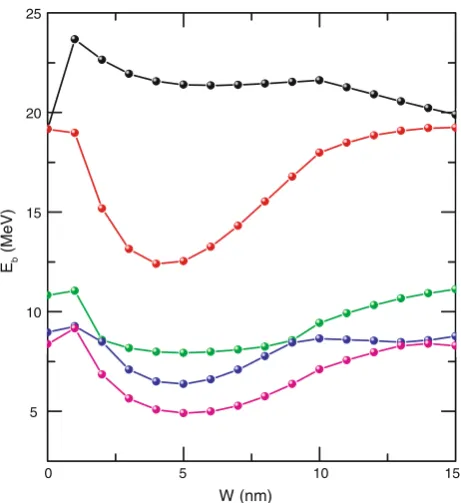
Figures1 and 2 show the first five energy levels and binding energy levels of an impurity in a QW as functions of the QW width W for an acceptor at the QW center. Figure1 shows that the energy levels monotonically and quickly decrease as the well width increases. It is well known that the donor binding energy has a peak as the QW width increases. However, Fig.2shows that the changes of the acceptor binding energies are very complex as the QW width W increases. This is because the holes have asym-metric effective masses, and there are mixing effects between heavy- and light-hole states.
Figure3shows the binding energy levels of the first five states as functions of the donor position z0 for the QW
width W = 10 nm. This figure shows that the binding energies monotonically decrease as the acceptor moves away from the QW center.
10 5
0 15
0 50 100 150 200
En
1 (MeV)
W (nm)
Fig. 1 The energy levels of the first five states as functions of the QW widthWfor an acceptor at the QW center
5
0 5 10 15
10 15 20 25
W (nm)
Eb
(MeV)
Fig. 2 The binding energy levels of the first five states as functions of the QW widthWfor an acceptor at the QW center
0
0 1 2 3 4 5
5 10 15 20 25
Eb
(meV)
Z0 (nm)
W = 10 nm
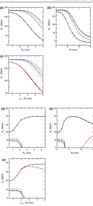
[image:3.595.310.541.56.308.2] [image:3.595.311.540.431.684.2]Figure4a and b shows the impurity energy levels of the first five states as functions of the square QWW side length L0(a) and the cylindrical QWW radius.(b) for an acceptor
at the QWW center. Compared with Fig.1, we find from Fig.4 that the impurity energy levels decrease slowly as the QWW size increases. This is because the acceptor is confined in two directions.
Figure5a and b is the same as Fig.4a and b, respec-tively, but are for the binding energy levels instead of the
impurity energy levels. The binding energy of the acceptor in the QWW is larger than that in the QW because the quantum confinement effects in the QWW are larger than in the QW.
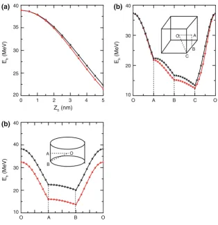
Figure6a and b shows the binding energy of the first five states as a function of the impurity position for a square QWW with side width L0 = 10 nm (a) and for a
cylindrical QWW with radius.¼5 nm (b). The positions of O, A, and B in Fig.6a are indicated in the inserted -50
0 5 10 15 1 2 3 4 5
0 50 100 150 200
(a) (b)
0 50 100 150 200
En 1 (MeV)
En 1 (MeV)
L0 (nm) ρ0 (nm)
Fig. 4 The impurity energy levels of the first five states as functions of the square QWW side lengthL0(a) and the
cylindrical QWW radius.(b) for an acceptor at the QWW center
0
0 5 10 15 1 2 3 4 5
10 15
5 20 25 30 (a)
Eb
(MeV)
0 10 15
5 20 25 30 (b)
Eb
(MeV)
L0 (nm) ρ0 (nm)
Fig. 5 The same as Fig.4but for the binding energy levels of the first five states
O
B A
0
O A B O 0 1 2 3 4 5
10 15
5 20 25 30 (a)
Eb
(MeV)
0 10 15
5 20 25 30 (b)
Eb
(MeV)
x0 (nm)
Fig. 6 The binding energy of the first five states as functions of the impurity position for the square QWW side lengthL0 =
[image:4.595.235.545.58.215.2] [image:4.595.232.545.363.711.2]1 2 3 4 5 0 5 10 15 200
180
100
50
0 (a)
En
1 (MeV)
200
150
100
50
0 (b)
En
1 (MeV)
R0 (nm)
1 2 3 4 5
200
150
100
50 (c)
En
1 (MeV)
W (nm)
ρ0 = W (nm)
Fig. 7 The impurity energy levels as functions of the spherical QD radiusR0(a), the
square QD side widthW(b), and the cylindrical QD radius.0
and heightWð.0¼WÞ(c) for
an acceptor at the QD center
1 2 3 4 5
1 2 3 4 5
50
40
30
20
10
0 (a)
Eb
(MeV)
40
30
20
10
0 (c)
Eb
(MeV)
R0 (nm)
ρ0 = W (nm)
0 5 10 15
50
40
30
20
10
0 (b)
Eb
(MeV)
W (nm)
[image:5.595.235.541.39.717.2]figure. From this figure it is easy see that the binding is the weakest for the impurity located at the corner of the square QWW.
Figure7(a), b, and c gives the impurity energy levels as functions of the spherical QD radiusR0(a), the square
QD side length W (b), and the cylindrical QD radius .0
and height W (.0¼W) (c) for an acceptor at the QD
center. Compared with Figs.1 and 4, we find that the impurity energy levels decrease more slowly in the QD than in the QW or the QWW. This is because the quan-tum confinement effect is larger in the QD than in the QW and QWW.
Figure8a, b, and c is the same as Fig.7a, b, and c, respectively, but are for the binding energy levels. From Fig.8(a), we find that there is only one binding energy for which R0 is greater than about 2.2 nm. The first two
quantum states are degenerate and correspond to the first energy level, due to the symmetry of the spherical QD. Figure8(b) shows that there is only one binding energy level when the side length is between 3 and 10.5 nm. If the side length is greater than 10.3 nm, the second binding energy level arises once again. Figure8(c) shows that the first two binding energy levels diverge quickly, and the other binding energy levels disappear as the QD radius and height become larger than about 2.5 nm.
Figure9a, b, and c shows the binding energy as a function of the impurity position with a spherical QD radius ofR0 = 5 nm (a), with a cubic QD side length of W = 10 nm (b), and a cylindrical QD radius.0and height Wequal to 5 nm (c). The impurity positions of O, A, B and C in Fig.9b and c are indicated on the inserted QD figure, respectively. As the acceptor moves away from the center, the symmetry decreases, the degeneracy is lifted, and the binding energy level splits into two branches. Figure9c shows that there are two binding energy levels when the cylindrical QD radius .0 and height W equal 5 nm. The
binding energy is the largest when the impurity is at the QD center, and it is least when the impurity is at the corner.
Conclusion
In summary, we have calculated the electronic structures and binding energy levels of a hydrogenic acceptor impu-rity in 2, 1, and 0-dimensional semiconductor nano-structures in the framework of effective-mass envelope-function theory. Our method can be widely applied in the calculation of the electronic structures and binding energy levels of a hydrogenic acceptor impurity in semiconductor nano-structures of other shapes and other semiconductor
O A
B
O A
B
C
0 1 2 3 4 5
20 30
25 35 40 (a)
Eb
(MeV)
Z0 (nm)
O A B C O
10 20 30 40 (b)
Eb
(MeV)
O A B O
10 30
20 40 40 (b)
Eb
(MeV)
Fig. 9 The binding energy as a function of the impurity position with the spherical QD radius of
R0= 5 nm (a), with the cubic
QD side lengthW = 10 nm (b), and the cylindrical QD radius.0and heightWequal to
[image:6.595.230.545.55.380.2]material systems. One only needs to specifyV(r) and other material parameters. External field effects are also easily considered with this method.
Acknowledgments This work was supported by the National Nat-ural Science Foundation of China under Grant Nos 60325416, 60521001, and 90301007.
References
1. A.D. Yoffe, Adv. Phys.51, 1 (2001)
2. G. Mahieu, B. Grandidier, D. Deresmes, J. P. Nys, D. Stievenard, Ph. Ebert, Phys. Rev. Lett.94, 026407 (2005)
3. B.A. Bernevig, S.C. Zhang, Phys. Rev. B71, 035303 (2005)
4. S. Loth, M. Wenderoth, L. Winking, R. G. Ulbrich, S. Malzer, G.H. Dohler, Phys. Rev. Lett.96, 066403 (2006)
5. J. Kundrotas, A. Cerskus, S. Asmontas, G. Valusis, B. Sherliker, M.P. Halsall, M.J. Steer, E. Johannessen, P. Harrison, Phys. Rev. B72, 235322 (2005)
6. F. Buonocore, D. Ninno, G. Iadonisi, Phys. Rev. B62, 10914 (2000)
7. C.M. Lee, W.Y. Ruan, J.Q. Li, R.C.H. Lee, Phys. Rev. B71, 195305 (2005)
8. V.I. Galiev, A.F. Polupanov, Semiconductors,27, 663 (1993) 9. P. Janiszewski, M. Suffczynski, Acta Phys. Pol. A 88, 1171
(1995)
10. J.I. Climente, M. Korkusinski, P. Hawrylak, J. Planelles, Phys. Rev. B71, 125321 (2005)
11. M.A. Cusack, P.R. Briddon, M. Jaros, Phys. Rev. B54, R2300 (1996)