© 2017, IRJET | Impact Factor value: 6.171 | ISO 9001:2008 Certified Journal | Page 1123
A High Gain Boost Converter for PV Power System Applications
Anu Ramabhadran M A
1, Harikumar R
21,2 Department of Electrical and Electronics Engineering, Ilahia College of Engineering and Technology,
Mulavoor P O, Muvattupuzha, Kerala, India
---***---Abstract -In this paper, a high gain DC/DC boost converter is presented. The presented converter consists of a power switch, a coupled-inductor and four diodes and capacitors. The presented converter is based on the conventional basic SEPIC converter. A voltage multiplier cell is used for the purpose voltage gain. The leakage current of the coupled inductor is recycled by the passive clamp circuit, so the voltage spikes on the power switch are minimized. In addition, the voltage stress on the power switch is reduced. Therefore the efficiency of the conversion is increased due to the low switching loss. The simulation results are provided by the MATLAB/Simulink Software. The closed loop simulation of proposed converter is done using PI controller with an input of 20V and output obtained is 240V DC.
Key Words: DC/DC Converter, High gain converter, Boost Converter, PV Power System Applications, etc…
1. INTRODUCTION
Renewable energy resources have the wide role in the field of power electronics research. The photovoltaic cells which give a very low output voltage, are used in most of the applications.The DC-DC boost converter has to be connected with the renewable energy source in order to increase the available voltage for various high voltage applications. Different topologies have been introduced to achieve a very high voltage gain which doesn’t include the method of increasing the duty cycle. By combining switched inductors, coupled inductors with the classical boost converter, a high frequency transformer or switched capacitors with high step up ratio and a low voltage stress can be obtained [5].
Due to the vast improvements in semiconductor technologies, power electronic devices are now widely used in various applications [1, 2]. DC/DC converters are among the power electronic devices which are generally available in applications such as LED drivers, renewable energy sources, battery chargers and so on [3]. Renewable energy sources are very favorable because they are abundant and pollution free. The most important renewable energy sources are photo voltaic panels (PVs), fuel cells (FCs) and wind energy. The output power of the PV panels is highly dependent on the environmental conditions for instance temperature, irradiance level and unexpected shadows [4, 5]. The output voltages of these sources are low DC voltage. Therefore, suitable converters are required to boost the low DC voltage. It can be then connected to the grid via a grid-connected inverter.
The output voltage of the PVs are between 24-40V. The DC-link voltage of the inverter must be at least 400V in order to connect the inverter to the load/grid. Series connection of the PV panels is the easiest solution. However, there are some disadvantages such as in partial shading condition. Therefore, it is very efficient to use a DC/DC converter for each PV panel. This method, known as distributed MPPT (DMPPT) can be implemented using various DCIDC converters [6] or micro inverters [7]. In this case, the converter must have some especial characteristics such as the high output voltage gain.
Isolated converters using transformers with large tum ratio can also have high voltage gain. However, these converters have poor performance and low conversion efficiency due to leakage inductance and the parasitic capacitance formed by the secondary winding of the transformer which causes voltage and current stresses [10, 11]. In [12], quadratic converters are also presented which are actually two conventional converters in cascade. Therefore, they are not very efficient in processing energy. Some novel structures of high step up converters are also presented in [14, 15]. The DMPPT method can be implemented using all structures mentioned above. However, the implementation cost would increase dramatically if a converter is employed for each PV module.
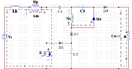
2. A HIGH GAIN DC/DC BOOST CONVERTER
© 2017, IRJET | Impact Factor value: 6.171 | ISO 9001:2008 Certified Journal | Page 1124 Fig -1: Proposed high gain converter
3. OPERATION PRINCIPLE OF PROPOSED CONVERTER
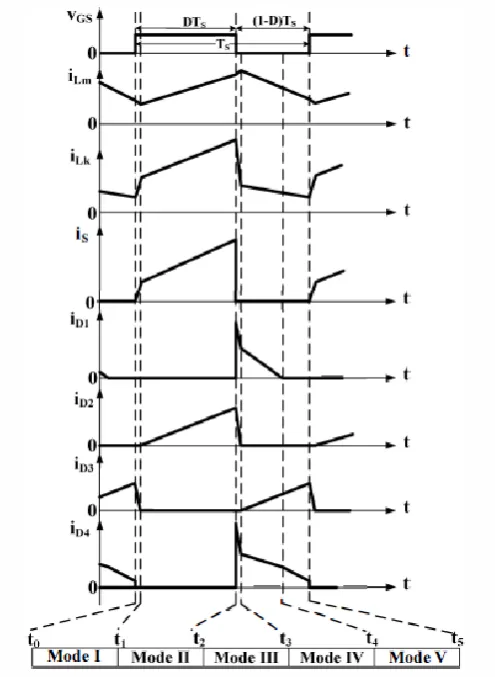
The proposed topology consists of a power switch, a coupled-inductor, 4 capacitors and 4 diodes. To simplify the analysis of the converter, the ripples of the capacitor voltages are neglected. In addition, all the components are ignored. In renewable power system applications, the input power sources should be operated in continuous conduction mode (CCM). For instance, in PV power systems, a main purpose is to minimize the current ripple in order to set their output power on reference value. Therefore, in this paper, steady state and dynamic behavior of the converter have been analyzed in CCM. The steady-state and dynamic analyses of the proposed converter are explained as follows. There are five operation modes in the CCM operation of the converter.
3.1 Mode I:
[image:2.595.315.559.83.228.2]In this time interval diode D3 and switch S are turned on as shown in Fig.2 . The magnetizing and leakage inductors are charged by the input source. Capacitor C3 is charged by the secondary side current of the coupled inductor. The output capacitor is discharged to the load. This mode ends when the inductor currents iLk and iLm become equal.
Fig -2: Mode I operation of converter
3.2 Mode II:
In this interval switch S and diode D2 are turned on. The magnetizing and leakage inductors are charged by the input sources. Capacitor C1 is charged by the secondary side current of the coupled inductor and the energy stored in
[image:2.595.315.557.477.603.2]capacitor C2. The output capacitor provides energy to the load. This mode ends by turning switch S off.
Fig -3: Mode II operation of converter
In the second operation modeas shown in Fig.3, the voltage on the magnetizing inductor is as follows:
VLm = VI (1)
In addition, the following equation can be written in mode II.
VC1 = VC2 + nVLm (2)
3.3 Mode III:
In this mode, switch S is turned off as shown in Fig.4. Diodes D1, D2, and D4 are turned on. The leakage inductor current is decreased linearly. Capacitor C1 is charged through diode D1 Capacitors C1 and C3 are discharged to the load through diode D4. This mode ends when the magnetizing and leakage inductor currents become equal.
Fig -4: Mode III operation of converter
3.4 Mode IV:
[image:2.595.47.264.551.664.2]© 2017, IRJET | Impact Factor value: 6.171 | ISO 9001:2008 Certified Journal | Page 1125
Fig -5: Mode IV operation of converter
The voltage on the magnetizing inductor is as below:
VLm = - VC3 = VI – VC2 (3) n
In mode IV, the following voltages can be expressed:
VO = VC1+ VC2 + VC3 (4)
3.5 Mode V:
[image:3.595.50.281.431.562.2]In this mode diodes D3 and D4 are turned on. The magnetizing and leakage inductor currents are decreased linearly. Capacitor C3 is discharged to the load. Capacitors C1 and C3 are discharged to capacitor the load. This mode ends by turning switch ‘S’ on again.
Fig -6: Mode V operation of converter
In mode V, the following equation, according to Fig. 6, can be derived:
Vo = VC1 + VI +VC3 – VLm (5)
By applying the voltage-second balance on the magnetizing inductor, the voltage of the capacitor C3 can be calculated:
VC3 = nDVI (6) 1-D
By substituting (6) into (3) and simplifying the equations, the voltage of the capacitor C2 can be expressed:
VC2 = VI (7) 1-D
According to (2) and (7), the voltage of the capacitor Cl will be written:
VC1 = (1=n-nD) VI (8) 1-D
VO = (n+2) VI (9) 1-D
‘n’ is the turns ratio of coupled inductor.
The typical waveforms of the proposed converter in steady state are depicted in Fig. 7.
Fig -7: Waveform of converter in Continuous Conduction Mode
4. SIMULATION RESULTS
© 2017, IRJET | Impact Factor value: 6.171 | ISO 9001:2008 Certified Journal | Page 1126 Table -1: Parameters used in simulation
Parameters Values
Input Voltage 20V
Output Voltage 240V Coupled Inductor n=3 Switching Frequency 50kHz
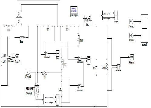
The closed loop simulation of proposed converter is shown in Fig.8.
[image:4.595.312.559.309.441.2]Fig -8: Simulation of converter (Closed Loop)
Fig -9: Closed loop feedback of Proposed Converter
Simulation outputs waveforms are shown Fig.10. The output voltage is 240 V, Input voltage is 20V.
Fig -10: Output waveform of Proposed Converter
Fig -11: Waveform of voltage and current across switch
The voltage and current cross the power switch and diodes are shown in Fig.11 and Fig.12.
[image:4.595.33.267.446.539.2]
Fig -12: Waveform of voltage and current across diode
5. CONCLUSION
In this paper, a high gain DC/DC boost converter has been proposed. The proposed converter has various advantages such as high voltage output gain and low voltage stress. The efficiency of the presented converter is high because the coupled-inductor leakage current is restored. The detailed analysis of the converter has been discussed. The closed loop simulation has been carried out by the MA TLAB/Simulink Software. The obtained results have shown that the presented converter has a proper, favorable and efficient.
REFERENCES
[1] Amir Farakhor and Hossein Ardi, “Analysis and Design
Procedure of A Novel High Voltage Gain DC/DC Boost Converter,” 8th Power Electronics, Drive Systems & Technologies Conference (PEDSTC 2017), 14-16 Feb. 2017.
[2] Jansen Kai, W., Varvar, A: 'The development of low cost
[image:4.595.35.286.613.725.2]© 2017, IRJET | Impact Factor value: 6.171 | ISO 9001:2008 Certified Journal | Page 1127
[3] Gao, 1., Dougal, R., Liu, S., Iotova, A: 'Parallel-connected
solar pv system to address partial and rapidly fluctuating shadow conditions'. IEEE Trans. Ind. Electron., 2009., 56, (2), pp. 1548-1556 .
[4] A Ajami, H. Ardi, and A Farakhor, "Design, analysis and
implementation of a buck-boost DC/DC converter,"lET Power Electron., vol. 7, no. 12, pp. 1755-4535, Dec. 2014.
[5] H. Ardi, A Ajami, F. Kardan, and S. N. Avilagh, "Analysis
and implementation of a non-isolated bidirectional DC/DC converter with high voltage gain," IEEE Trans. Ind. Electron., vol. 63, no. 8, pp. 4878 -4888, April 2016.
[6] A Ajami, H. Ardi, and A Farakhor, "A novel high step-up
DC/DC converter based on integrating coupled inductor and switched-capacitor techniques for renewable energy applications," IEEE Trans. Power Electron., vol. 30, no. 8, pp. 4255-4263, Aug. 2015.
[7] R. B. Mohammad, H. Ardi, R. Alizadeh, A. Farakhor, "Non
-isolated multi-input-single output DC/DC converter for photovoltaic power generation systems," lET Power Electron., vol. 7, no. II, pp. 2806-2816, Nov. 2014..
[8] S. M. Chen, T. 1. Liang, L. S. Yang, and 1. F. Chen, "A Boost
Converter with Capacitor Multiplier and Coupled Inductor for AC Module Applications," IEEE Trans. Ind. Electron., vol. 60, no. 4, pp.1503-1511, Apr. 2013.
[9] Tseng, S.Y., Ou, C.L. "Interleaved coupled-inductor boost
converter with boost type snubber for PV system" Energy Conversion Congress and Exposition, Tao Yuan, Taiwan, September 2009, pp. 1860-1867.
[10] S. K. Changchien, T. J. Liang, J. F. Chen, and L. S. Yang,
"Step-up DCDC converter by coupled inductor and voltage-lift technique," IET power. Electron., vol. 3, no. 3, pp. 369-378, May. 2010.
[11] Trishan, E., Patrick, L. "Comparison of photovoltaic array
maximum power". IEEE Trans. Energy Convers., 2007, 22, (2), pp. 439-449
[12] H. Ardi, R. Reza Ahrabi, and S. N. Ravandanagh,