Unit(~d States Patent
[19]Friend et aI.
[54] DIGITAL INFORMATION SWITCHING
SYSTEM
[75] Inventors: George E. Friend, Dallas; John D. Meyers, Plano; Steve Van Dyke, Dallas; James R. Carreker, San An-tonio, all of Tex.
[73] Assignee: Datapoint Corporation, San Antonio, Tex.
[21] Appl. No.: 248,821
[22J Filed: Mar. 3, 1981
[51J Int. Cl) ... G06F 11/20; G06F 3/04 [52J U.S. Cl ... 364/900; 370/58; 370/67; 371/9; 371/10 [58J Field of Search ... 364/200 MS File, 900 MS File; 370/58, 67; 371/9, 10
[56] References Cited
U.S. PATENT DOCUMENTS
4,145,734 3/1979 Bienvenu ... 364/200 4,322,843 3/1982 Beuscher et a!. ... 370/58
r
-12
RSU
[II]
[45]
Primary Examiner-Raulfe B. Zache
4,442,502
Apr. 10, 1984
Attorney, Agent, or Firm-Antonelli, Terry & Wands
[57] ABSTRACT
A digital information switching system features modu-lar design with dispersed processing in which data is switched locally in one of a plurality of remote switch-ing units for connection between local terminals, and data to be exchanged between terminals connected to different remote switching units is switched in a central switching unit, which is connected to the remote switching units by way of interswitch links. Both the central switching unit and the remote switching units are of the same general configuration being individually processor controlled. Reliability of each unit in the system is enhanced by diagnostic and maintenance fea-tures including provision of redundant devices in each unit, detection of device failures, automatic replacement of failed devices with redundant devices and communi-cation of the failure to a remote service center.
29 Claims, 17 Drawing Figures
- - - - 1 /
-II
1
('4
1 2I
i---~:-l
' , MI~~g.:iVE
I
C.O TRUNKS
',RADIO
,
12
RSU COAXIAL CABLE
UP TO 6 RSU'S PER
C~U
14
"
"OPTICAL
/' OATA
/' \ LINK
14
CSU
10
I
II
I
I
I
I
I
RSU
I
I
AND 12I
TIE LINES
---'-'----'-1
~ SWITCHING~ SUBSYSTEM
L __
---.J'-3L _ _ _ _ _ _ _ _ _ _
J
I
I
1
I
I
DATA 1L
MANAGEMENTJ
_ SUBSYSTE~ _
-r---=J
,-- ---
- - - - I
/~I
I
TERMINAL.
12r
I :
I
, RSU
('4
I
I
TERMINAL , DIGITAL 'II
I
'
',RADIO MICROWAVEI\r-TER-MINA--'L
I, :
i
I
r
'2
b-fI:
I
•
RSU COAXIAL CABLE CSU
II
'--
_TE_RM_'N_AL_II - II
•
•
14
10
I
I
I
I
RSU'S PER UP TO6
CSU•
, /
/OPTICAL / DATA
I,
TERMINALII :
, ,
I
I
j
•
,/ \ LINK 14I
I
I
I
C.O •TRUNKS
I
TIE LINES AND ~L
~3_ _
.---J
I -
I
I
12
SWITCHINGI
1
L
SUBSYSTEM_________ J
RSU
FIG I
I
DATAL
MANAGEMENTJ
SUBSYSTEM-C!
.
til
.
~
~
(1)
::s
f""t- )0-"0 !"'
-9
-
\0~
tI)
::r
(I) (I)
--
o
....,
-
IV,J::..
...
,J::..
,J::..
tv
...
U\
o
r
-I
I
I
I
I
I
I
I
I
~c,':)
SYSTEM PROCESSOR
Lso
/"c,,:>
SYSTEM
PROCESSOR RAM
;
CONTROLLER BUS
/":Ju :JU'\
RAM
;
~
1
TERMINAL
l..J4S
BUSINTERFACE
---. -. -l
Z BUS Z BUS __
3:5, •
-. f-r",
t
(3S'
MMI BUS MMI PROCESSOR CONTROLLER PROCESSOR
:
*
Sl
:
CONTROL
MODEM PANEL
t
"tv. I
BUS
CONTROLLER.
I
I
I
I ;
vJS
C.O.
I
I
I
I
) COl
IS/
L..:....:..
- - - -
~OLLER ~-/"65 TERMINAL BUS
~
TRUNK
-
-- --
- -
-,
ISL
V
70
INTERFACE&
•
'-66
(67
7 5
-§
PORT PWA8 PORTS / DEVICES
I
1
EXPANDER
XMT PCM BUS
RCV PCM BUS
@]
PORT PWA8 PORTS/ DEVICES
I
, (75
1
EXPANDER EXPANDER MATRIX
...
c
.
CZl
.
~
~
(D
a
~
:;
...
9
...
\0
00
~
en
::r
('II ('II--tv
o
"""l
...
tv
~
'"
~~
N
'"
til
16 ...
\
FIG. 3
- - - ' - -
-
-
-!cONTROLLER
-
- - - -
---,
/
•
I
SYSTEM•••
SYSTEMRAM RAM
MMI
(35
• L
35'
BUS MMI BUS
•
I
I
256
K•
••
I
PROCESSOR PROCESSORWORD
256
KCONTROLLER
WORD PROCESSOR PROCESSOR CONTROLLER
I
I
I
I
:
:
:
:
:
I
CONTROLLER BUSL50
I
I
(45
(60
,
) 5
48
I
DMS / TAPE/OJ
COAX
~
TERMINAL BUSH
0-0
r
CONTROL MODEMI
\
INTERFACE PANEL C.O4 CARTRIDGE TRUNK
L_r-- _________
~_ _
-':'APE _ _ _ _ _ _ _ _ _ _ _ _ _r
TERMINAL BUSL.65
XMT PCM BUS
OMS
l.66
RCV PCM BUS
(67
7 0 .
r
J
f
L2
r
/ CONFERENCE
ISL ISL CSU CSU
•••••
70--
INTERFACE INTERFACE BRIDGE MATRIX MATRIX1'85'
I .I I .I
..
•
, v---~/
4.096
MBITFULL DUPLEX ISL'S
j
I
I
I
I
~
~
.
en
.
;f
('D
::s
f""'to.
~
I--'
~O
I--'
\0
~
en
::r'
(1) (1)
-
VJo
P"O)I--'
N
~
...
~
~
N
...
U\
[image:4.798.56.727.88.508.2]-
-SUPV-
SUPVCLKt
~~
~ 1-18 ~ 1-18 18-
r---
18--..LOGIC LOGIC
C~-4
• • • • • • • • • • • • • •
LOGICCSb-4
~
X
~25
( ; '1"---25'"40
"--SW LSW XO-XI5)6
\SW-BCLK
/
-
""'\
RESET
/ PRSREQ
""'\
/
RDYI""'\
RDY2
"
t50
'-
PRIREQ - ,/"-
PRIGNT - ,/-'-
PHYS, /
ERR j
'-
. /SUPVCLK
FIG. 4A.
-SUPV1
I
X
X
X
r
X
X
/
START0
2 ; ; 4 CON ODD STOPBIT '- yo / PAR BIT CARD SLOT ADDRESS
~~---~'V
/
ACTlVE- LOW
FIG.
4.
t
~~
r-LOGIC
(\
I-I \SW
40'
c
.
en
•
~
a
("D=
...
~
-p
-\0
~
C".f.l
:r
('D ('D...
..j::..
o
...,
-tv
~
,..
~ ~
N
'"
U\
[image:5.797.79.738.86.548.2]~50
zaOOl, TIMING /CONTROL,
ADDRESS DECODE
A BUS ...L23
,
FIG.
5.
L
252
EPROM/RAM WITH
ERROR DETECTION/ CORRECTION
D BUS ~16
ERROR ADDRESS REGISTER
CONTROLLER BUS INTERFACE
AND
~
CONTROL
l256
l25a
L
254
MEMORY PROTECTION
*
INTERRUPT LOGIC
L
259
CONTROLLER BUS DRIVERS AND
BUS DISCONNECT
(--260
..
-SUPV SUPV CONTROLLER CLK BUS
*
Z-BUS INTERFACE
'---r--'\
255
Z-BUS
,
c
•
. tI'.l
.
~
a
o
a
~
-$=>
-\0
~
Vl
0-~ ~
...
U'I
[image:6.803.100.642.100.510.2]o
...,
...
tv
~
...
~ ~
tv
...
Ul
o
u.s.
Patent
Apr.
10,
1984
Sheet
6
of
12
4,442,502
>-~
0
~u
C\I
-w
LJ
a:
z
~u
.----W
..J
III
«
z
10
W1
~
10
='-T
a::
f----g
0
f----I
«
a:
~
'if.
-:!:
0
-U
C\I
f----C\I
~~~
If')
-~
--z-t7SJ
0
10
~
rt')
£SJ
a:
l
<[
--~
GSJ
~
T
-a:
Q..Q..
-0
ISJ
..J..J
IL.IL.
(/)
(lISJ
I\dnS
~
1
r
1
"V
~~3
./
~
....,
SAHd
""'-....,
IN~t~d
03~I~d
~
"V
./
GAO~
""'-S-::)
I"O~
~
/
~
"V
-03~S~d
~
13S3~
'-...
>llJ8
u.s.
Patent
Apr. 10, 1984
CONTROLLER BUS
RESET
BCLK
XO-XI5
PRSREQ
_ ROY I
RDY2
PRIREQ
PRIGNT
PHYS
_ ERR
FIG. 6.
-)6
,
T-BUS
.
INTERFACESheet 7 of 12
4,442,502
TSUPV
-TSUPVCLK
TCLK
TSTB
T-BUS TROY
TERR
_ ~ TAD0- 8 ~
-/9
PCMCLK (4.096 MHZ)
CS~-CS4 ~5 2XPCMCLK{8.19 2 MHZ)
,
SUPV PCMFSYNC
SUPVCLK
.
RECOVERED PC M CLK(4.096 MHZ)
-
t--45FIG. 9A.
61 62 63
I I
II
o
I 2 3 4"""'=""ISYNC"""-:-I MOw""-=-l
-r-=-I ""--:-1 -"--1 _-_ -___
~
= =
=
~ ~ ~ ~ ~ ~
~---
---
----.~.---DIGITIZED VOICE, PCM SAMPLES OR DATA
FIG 98.
[image:8.618.88.511.86.657.2]---u.s.
Patent
Apr. 10, 1984
- -
f><
z
u.
><
...J
<[
~
0~ ~
~
...J
U
l-I
J
LD
l-V)
'I
IX
J:
~
<[
0
~
IX
0
0
<[
IX
z
u.
Sheet 8 of 12
J~-
w
o
~O
ow
...JV) V) ZW
wO:
>0
- 0 0:<[
o
>-
jLD-0: 0:
W
l-I
4,442,502
0 0
ww
V)
I-V)u Ww
0: .... Ow 0 0 <[ >-0:
LDO
0: ~o:OW
...Ju.
~W
>U
~>
OW
FIG
8.
RG 10
ISL
CABLE
-TCLK
-TSTB
o
"
j '0r---~-TAD0 - 8
X
FNX
ADDx/ZZZZ07l:,?z!li
DATA HVZtY/I)/..
DATALX
FNX
ADDX
-TROY
zzLwIJ
I
I
J~~
tIm)
!
'---v---' ~
I
PRECHG
I
I
PRECHG
I
-TERR
7771117/IU
\
x:: x x:: x
VIIIII
'----v---" v '---y---./
RCV
..
..
~
XMIT
PRECHG DRIVEN LOW BY ADDRESSED PRECHG DEVICE IF ERROR DETECTED
701
702
RECEIVE XMTPCM BUS
/8
-
MOW/PCM 'PARALLEL PROCESSINGRCV DATA CCT
SIGNAL
/701
INTERFACE
.
TERMINAL BUSCCT
r
703
TRANSMIT
_ /8
MOW/PCMPARALLEL PROCESSING
XMT DATA CCT
-
RCVPCM BUSc
•
CIl
.
~
~
(D
a
~
!"1
-9
-\0
~
en
::r
(I) (I)
...
\0
o
....,
-N
,J::..
,.
,J::..
,J::..
tv
,.
Ul
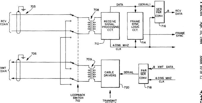
[image:10.799.75.738.86.533.2]FIG. II.
.
.
c:!
fJ)DATA (SERIAL) _
I
~
~
SER
~RCV
4""'t-CD
PAR DATA::s
CONV.4""'t-RCV
~
I I
r
~I
rl
RECEIVE FRAME~6
>
COAX I SIGNAL SYNC
PROCESSING LOGIC "t:S ;;
CCT. CCT.
-FRAME
P
SYNC·-
\0-714
I
00712---'
I
4.096 MHZ ~CLK
706
/
I I
en
709_
::r
CD CD
....
XMT
~
I I
I
L--o
~I~
~
I
,8 XMT DATA-
0COAX CABLE SERIAL
~~R~
0""'I)
DRIVERS
-CONV. 4.096 MHZ N
-CLK
,
h
720C;,8
1
.,J::;...LOOPBACK
,..
.,J::;...SWITCH .,J::;...
710 TRANSMIT
ENABLE
,..
N
U\
0
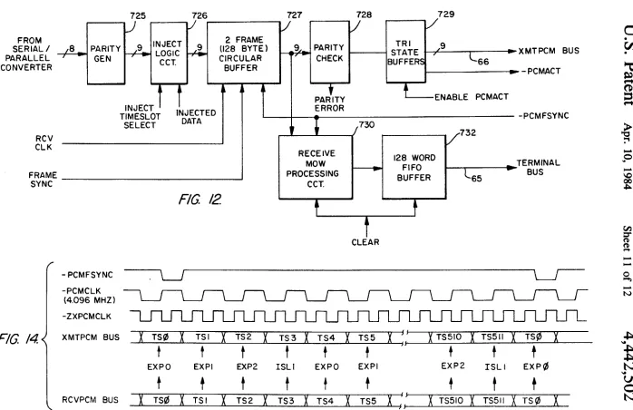
[image:11.798.61.743.146.494.2]FROM SERIAL/ PARALLEL CONVERTER
RCV CLK
FRAME SYNC
FIG. 14
725 726
727
LJ
tJ
1./-,8 PARITY
J9
INJECT2 FRAME
,
...
LOGIC~
(128 BYTE)GEN
'
[image:12.792.38.736.78.530.2]--9 ....
PARITY CCT. CIRCULAR...
CHECK BUFFER
INJECT
f
f
•
J
PAJTY
TlMESLOT INJECTED
ERROR
SELECT DATA
,
•
RECEIVE MOW PROCESSING
CCT.
J:I(;
I~EXPO EXPI EXP2 ISLI EXPO
t
t
t
t
t
RCVPCM BUS
X
TS0X
TSIX
TS2X
TS3X
TS4728 729
l/
V
TRI
STATE ,,9
BUFFERS L66
-. XMTPCM BUS
--
-PCMACTt
ENABLE PCMACT-PCMFSYNC 730
V
732
128 WORD
--
FIFOBUFFER L65
--TERMINAL BUS
t
-.-CLEAR
EXPI EXP2 ISLI EXP0
t
t
t
t
X
TS5X
I JX
TS510X
"~51IX
T s ¢ lc
.
c.n
.
~
~
f""t>
0
=
f""t>
€
:"'
...
P
...
\Q
00 ~
C/)
g-(1)....
...
...
o
...
...
N
~
--
~~
tv
--
U\
TO PARALLEL I
SERIAL CONVERTER
'G.
/3.
.OT T
r-'--M 0
/ N
- /8 T I
0
-740R
....
-MONITORED DATA
739
I
MOW MOW
DATA TRANSMIT
-PROCESSINGCCT.
f
CLJAR
(TS
Il
1
V
736COMBINE CCT.
j
(TS
0)
SYNC BYTEPCM DATA
(TS 2 -63)
738
/
128
WORD PARITY FIFO CHECKER BUFFER
1
,
PARITY ERROR
EVEN ODD PAR
t
RRrR
ERRPARITY CHECKER
•
GEN EVEN PARITY
...-735
737
-RCVPCM
:rERMINAL BUS
BUS
~
CI.l
•
~
~
f""'to-CD
=:s
f""'to-~
:-t
...
,.0
...
\0 00~
til
:::r
(I) (I)
-
...
N
~
...
N
~
,.
~ ~
N
,.
Ul
o
4,442,502
2
1
DIGITAL INFORMATION SWITCHING SYSTEM
BACKGROUND OF THE INVENTION
The present invention is directed in general to com- 5 munication systems, and more particularly, to a digital electronic communication management and informa-tion switching system which operates under dispersed microprocessor control to manage the interconnection, usage, record keeping and maintenance of various types 10 of conventional and specialized voice, data and facsim-ile terminals.
During the past decade, the emphasis in electronic system design has been on centralized control using computers of various size, degree of sophistication and 15 complexity. However, with the implementation and use of such systems over a period of time, concern has been expressed over various inherent disadvantages of the centralized processing system, including lack of flexibil-ity, obsolescence, and serious maintenance problems 20 which have literally rendered such systems totally unus-able in response to individual device failures within the system. On the one hand, complaints have been heard that a particular system was not capable of handling certain business office problems, having been designed 25 for general use in an effort to provide a universal prod-uct. On the other hand, even for those fortunate enough to obtain a system suitable for their specific needs, the problem of obsolescence presented itself only too quickly, especially in conjunction with systems that 30 could not be expanded. Finally, the problem of down-time in central processing systems presented the ulti-mate frustration since malfunction in the system gener-ally resulted in the entire system becoming disabled, therey rendering it totally useless until repairs could be 35 made. This interference with business was more than just an inconvenience to the businessman; it represented an unacceptable limitation on his ability to adequately serve his customers and clients and resulted in a serious
waste of manpower and other resources. 40
In an effort to overcome the above-mentioned disad-vantages in centralized processing systems, designers began to turn to modular concepts of system design, and with the significant advances in microprocessor devel-opment which brought a drastic reduction in the cost of 45 microprocessor manufacture, distributed processing within a system began to replace the centralized pro-cessing of prior years.
In additon, new types of systems began to be devel-oped. In the communication fields, the emphasis has 50 shifted toward digital systems. Thus, in the telephone industry, digital central office and private branch ex-change systems have been developed and made avail-able for use by the public. At the same time, new data communication systems involving the transmission of 55 all types of data and information in digital form have been developed. Systems have been developed for word processing as well as data processing and elec-tronic message functions in an effort to provide a more complete scope of services for the standard business 60 office or large corporation. These systems include not only electronic private branch exchanges, but also shared resource word processing and data processing systems; however, there has been a tendency to design such systems independently of one another, i.e., word 65 processing systems, data processing systems and tele-phone exchanges which are self-contained and designed specifically for those respective functions. Thus, the
business office typically may have a number of local networks and other computer resources providing data, text, and messages all flowing through or residing in respective systems in the form of a high volume of digitized information that must be accessed, sent, pro-cessed, managed and manipulated, as well as verbal information that needs to be communicated throughout the system. Such a situation calls for a communication hub or switching system into which the information can flow, be it data. text, voice or messages and be switched to its destination while simultaneously recording infor-mation on each transaction.
BRIEF DESCRIPTION OF THE INVENTION
A system is provided in accordance with the present invention in the form of a family of information switch-ing exchanges for effectswitch-ing the connections from person to person, from person to computer, and from computer to computer within the business office. In one aspect, the system of the present invention looks like an elec-tronic P ABX performing all of the voice functions normalIy associated with an electronic private auto-matic branch exchange. However, in another aspect this system integrates with terminals and with local net-works, bringing word processing, electronic message services and data processing into the office network as communities of interest. Thus, the system enhances existing dispersed data processing by using its power and speed to permit easy access to processing power through any compatible terminal and provides detailed reporting on alI information transactions, and ulti-mately, related costs, such as materials and labor, giving business organizations a degree of control and systems knowledge never previously available.
3
4,442,502
The data management system, which is connected to the central switching unit by a direct coaxial cable link, typically consists of a standard processor, printer and disc, which handles an assortment of administrative chores for the central switching unit including the col- 5 lecting of data on system usage as well as the assignment of class of service definitions to individual stations, rearrangement of extension numbers, or the implemen-tation of a customer least-cost routing table for the system, However, one of the major features of the data 10 management system insofar as its integra~ion with the telephone switching function of the system is concerned relates to the detailed reporting on costing, usage, and traffic provided thereby, Thus, the system provides a total integration of services relating to voice, data and 15 message services within a shared resource, processor dispersed system.
Because of its modular design and dispersed switch-ing architecture, the system of the present invention can easily handle growth and expandability. As a user's 20 requirements increase, each remote switching unit can be expanded in pace with that growth and additional remote switching units can be added where larger in-creases in system size are required. Telephone instru-ments can be added to the central switching unit 25 quickly since the data management system facilitates real-time, dynamic means of adding, changing, or mov-ing extension numbers, and the actual physical place-ment of terminals is transparent to the system, which allows them also to be changed or added as the user sees 30 fit. Features and functions are also easy to add and change, whether they are telephone instrument fea-tures, such as conference calling, or system feafea-tures, such as electronic message services. Both can be accom-plished by change to system table entries or the addition 35 of software modules with little or no change required in the system hardware.
In addition to the dispersed processing feature of the system of the present invention, unique maintenance features minimize risk of system failure. Self-diagnostic 40 maintenance procedures in each remote switching unit and central switching unit continually monitor the sys-tem, and if a problem occurs, the faulty circuit board is isolated, electrically disconnected and its spare is imme-diately enabled in an automatic manner within the sys- 45 tem without outside control. This occurs without inter-ruption to calls in progress, even if the failure is in a critical area, such as one of the computer microproces-sors, memories or switching matrix in the system. A diagnostic report is then automatically forwarded to a 50 central service center at which a message is printed out identifying the customer site, the type of product, which cabinet, which card cage, which card slot within that cage, what type of circuit board and the revision level of the board that failed. It is therefore possible to 55 dispatch a service representative in response to such an automatic communication with the correct replacement equipment to be installed while the system is in full operation.
It is a principal object of the present invention to 60 provide a digital information switching system which can fully integrate the functions of data processing, word processing, electronic message systems and voice, incorporating the principles of modular design, distrib-uted processing and automatic diagnostic and mainte- 65 nance features in a single digital information system.
It is another object of the present invention to pro-vide a digital information switching system which
uti-4
lizes dispersed architecture, dispersed data processing and local switching to permit system design for individ-ual user needs and the ability to expand in any aspect of the system in accordance with the user's future needs and requirements.
It is still another object of the present invention to provide a digital information switching system having a high degree of reliability through the use of self-diag-nostic features and the provision of individual redun-dant components, rather than redunredun-dant systems, to ensure continuous system operation without interrup-tion by component failures and automatic reporting of faults to ensure prompt maintenance and service of the system.
Another object of the present invention is to provide a digital information switching system that can inte-grate voice, data, facsimile, electronic and voice mes-sage services, graphics, word processing and coaxial-cable based local area data networks.
It is still a further object of the present invention to provide a digital information switching system having dispersed switching architecture which provides modu-lar, dynamic growth in terms of both system size and number and type of user functions and features.
These and other objects, features and advantages of the present invention will become more apparent from the following detailed description, when taken in con-junction with the accompanying drawings, in conjunc-tion with an exemplary embodiment of a digital infor-mation switching system.
BRIEF DESCRIPTION OF THE DRAWINGS FIG. 1 is a schematic block diagram of a digital infor-mation switching system in accordance with the present invention;
FIG. 2 is a schematic block diagram of a remote switching unit as embodied in the system of FIG. 1;
FIG. 3 is a schematic block diagram of the central switching unit as provided in the system of FIG. 1;
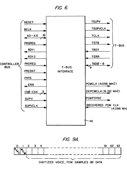
FIG. 4 is a schematic diagram of the controller bus arrangement as provided in both the remote switching unit and central switching unit in the system of FIG. 1;
FIG. 4A is a waveform diagram showing signals which appear in the control bus arrangement of FIG. 4; FIG. 5 is a schematic block diagram of a system or MMI processor of the type used in the central switching unit and remote switching unit;
FIG. SA is a schematic diagram of a typical control-ler bus device and its bus disconnect circuit;
FIG. 6 is a schematic diagram of the signal line con-nections to the terminal bus interface from the control-ler bus and the terminal bus;
FIGS. 7 and 8 are signal timing diagrams relating to write and read operations, respectively, on the terminal bus;
FIG. 9A is a diagram showing the data frame format on the interswitch link;
FIG. 9B is a diagram showing the message format on the multiplexed orderwire channel;
FIG. 10 is a general block diagram of the ISL inter-face;
FIG. 11 is a schematic diagram of the signal interface circuit in the ISL interface;
FIG. 12 is a schematic diagram of the receive MOW /PCM processing circuit in the ISL interface;
5
4,442,502
FIG. 14 is a timing signal diagram showing the man-ner of time slot allocation on the PCM buses.
6
and a selected time slot in an outgoing interswitch link 14. This is accomplished by a single-stage, strictly non-blocking time slot interchange network, which ensures that a path is always available through the switch. In a DETAILED DESCRIPTION OF A PREFERRED
EMBODIMENT
5 similar manner, switching is also provided in each of the remote switching units between terminal units or de-vices connected thereto, and this switching is again accomplished by a single-stage, strictly non-blocking The present invention provides an ;til-digital
switch-ing system which treats all signals to be switched as digital data. Signals, such as telephone conversations, which exist in the outside world in analog form are changed to digital quantities at the point of connection 10 to the system, and carried throughout as digital data. Signals from digital data terminals are brought into the system, switched and transmitted without conversion to analog form. Control information, from voice lines, data circuits and process control system connections, is also 15 brought directly into the system if originally digital in form, or converted to digital form at the system inter-face and processed in that form internally.
As shown in FIG. I, the system is divided into three basic parts: a switching subsystem I, a data management 20 subsystem 2 and a set of terminals 3. The switching subsystem 1 performs necessary format conversion of information signals exchanged between the terminals 3, senses and produces control signals, such as dial pulses for the terminals 3, and routes the information signals, 25 i.e., switches the call or connection. The data manage-ment subsystem 2, which is connected to the switching subsystem 1 via an interprocessor bus 4, stores data used to direct the switching subsystem 1 and stores records produced by operation of the system, such as call billing 30 information. Data required to configure the system to a particular customer's requirements is entered and up-dated using terminals and software provided in the data management subsystem 2. While in its broadest sense the present invention provides for the interconnection 35 of any known data management subsystem to the switching subsystem 1 via an interprocessor bus 4, one particularly-suitable system for this purpose is the At-tached Resource Computer (ARC) system, manufac-tured and sold by the assignee of the present invention. 40
The system illustrated in FIG. 1 controls and inter-connects a variety of traditional terminals 3, such as rotary or pushbutton telephones, as well as contempo-rary terminals, such as electronic telephone sets and directly-connected digital data terminals. The system 45 may also interact directly with the terminal or provide
time slot interchange network in the remote switching unit 12 itself. Sensing and control for the terminals 3 is performed over a separate digital internal control path common to all terminal units or devices and which extends to the central switching unit 10 over the inter-switch links 14.
Directory information including names and corre-sponding directory numbers, connection information including directory numbers versus physical port loca-tions, class of service data, and all data related to re-cord-keeping are supplied from the data management subsystem 2 and maintained in the central switching unit 10 of the switching subsystem 1. Each central switching unit 10 can connect to sixty remote switching unit connections, and, with each remote switching unit 12 being connected to the central switching unit 10 via one or more interswitch links 14 and each remote switching unit supporting up to 384 terminals, the over-all system as seen in FIG. 1 could serve as many as 23,800 terminals overall. On the other hand a system of as few as 200 terminals may also be provided. As will be described in greater detail herein, the concentration of the ports to the interswitch links 14 in accordance with the present invention is variable depending on the con-figuration of the remote switching units 12, making possible completely non-blocking switching to the cen-tral switching unit 10 under various switching configu-rations.
The terminals 3 which may be attached to the system are of two basic types: user terminals and system termi-nals. User terminals interact directly with the user and his equipment, such as data processing or facsimile ma-chines, while system terminals connect the system to public and private networks, or enable attendant and maintenance technician control of the system. The sys-tem supports various types of user terminals, including conventional single line station sets, conventional mul-tibutton key sets, electronic telephones and various standard data units which allow direct input of digital data and associated control information at rates of up to 56,000 bits per second. Terminals to connect the system a path between two or more compatible terminals using
addressing and connection information supplied by the terminals in accordance with customer's data base as stored in the data management subsystem 2.
Switching of voice andlor data information is pro-vided by the switching subsystem I, which is formed by
50 to all common central office and tie trunks are also provided.
As system terminals, there may be provided attendant consoles, a maintenance terminal and a remote diagnos-tic center. These terminals interface with the switching subsystem 1 in the same manner as the user terminals. The particular terminal which provides digital data to the system is transparent at the interface to the switch-ing subsystem I, the system receivswitch-ing data from any of these terminals 3 without regard to the type of terminal involved.
FIG. 2 is a more detailed block diagram of a typical remote switching unit 12 as provided in the system of FIG. 1. The remote switching unit 12 provides low level interface, processing and local switching for the a combination of distinct units including a central
switching unit 10 and one or more remote switching units 12. The central switching unit 10 provides inter- 55 connection among multiple remote switching units 12, controlling the set up and progress of all connections through the switching subsystem 1. The central switch-ing unit 10 is also the connection point for the data management subsystem 2 via the interprocessor bus 4. 60 Connections to the central switching unit 10 from each remote switching unit 12 are effected via one or more interswitch links (lSL) 14, which may take the form of coaxial cable, digital microwave radio link, optical data
link, or a standard Tl PCM span link, for example. 65 connected stations, trunks, electronic instruments, at-tendant consoles and common control electronics con-nected as terminals thereto. Conversion between analog voice signals and industry standard digital format and Switching in the central switching unit 10 of an
7
4,442,502
concentration of the devices in accordance with the time slots provided by the interswitch links 14 are also accomplished in the remote switching unit 12.
The heart of the remote switching unit 12 is formed by a controller 16 which comprises one or more system 5
processors 25, random access memory units 30, mainte-nance management interface (MMI) processors 35, bus controllers 40, terminal bus interfaces 45 and a bidirec-tional controller bus 50, which interconnects these ele-ments, providing for exchange of data, address and 10
control signals therebetween. The controller 16 addi-tionally includes a modem 55 connected to the bus con-trollers 40 for effecting automatic communication relat-ing to the detection of faults within the system to a remotely-located central service area via a central of- 15 fice trunk, and a control panel 60, which is also con-nected to the bus controllers 40, is provided to effect interface by maintenance personnel with the system.
The controller 16 communicates with a terminal bus 65 via the terminal bus interface 45 and it is over Z 20
terminal bus 65 which sensing and control data mes-sages to and from the system processors 25 and termi-nals 3 are carried. Connected to the terminal bus 65 are one or more ISL interfaces 70, expanders 75 and switch-ing matrices 85, the expanders 75 in turn each beswitch-ing 25
connected to a plurality of port interface circuits having outputs extending to a plurality of ports associated with the terminals 3. In addition to the terminal bus 65, a transmit PCM bus 66 and a receive PCM bus 67 inter-connect the matrix 85 with the expanders 75 and the 30 ISL interface 70.
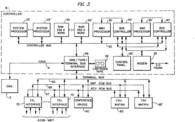
As seen in FIG. 3, the central switching unit 10 is virtually identical to the remote switching unit 12. One difference between these units resides in the fact no expanders 75 are provided in the central switching unit 35 10; instead, additional ISL interface circuits 70 (up to thirty) and a conference bridge 90 are connected to the buses 65, 66 and 67. In addition, the terminal bus inter-face 45 in the controller 16 provides for connection to the data management subsystem 2 via the interprocessor 40 bus 4, as well as to a cartridge tape unit 48, which pro-vides local non-volatile storage of the on-line program and data base for the central switching unit 10. Other-wise, the units 10 and 12 are the same. Thus, to facilitate the description of the present invention, only a detailed 45
description of a remote switching unit 12 will be pres-ented herein, it being understood that such description is also applicable to the components and function of the central switching unit 10.
The heart of the controller 16 as provided in any of 50 the switching units 10 and 12 is the multiconductor controller bus 50 which provides for interconnection of the various devices which make up the controller, such as the system processor 25, memory 3D, MMI processor 35 and the terminal bus interface 45 by which the con- 55 troller bus interfaces with the terminal bus 65. The operation of the controller bus 50 is based upon a con-cept of physical and logical identification, with each card edge connector position being provided with a unique 5 bit card slot address via etch patterns which 60 are unique to that position. The logical address of any device is a dynamic value assigned by the MMI proces-sor 35 at system initialization/configuration or as a re-sult of reconfiguration caused by failure of some device. This value is stored in a logical address register within 65 the device and is used by the device for all normal communication with other devices on the bus 50. How-ever, the physical addresses permit direct addressing of
8
the bus slot portions, facilitating the assigning of logical addresses and the selective replacement of active de-vices on the bus in response to failures.
Communication between devices connected to the controller bus 50 is on a request/grant basis, under supervision and control of the bus controller 40. Re-quests for bus access are arbitrated by the bus controller
40 and access is granted for a single bus operation to a processor 25 or other device which can request bus access for a data transfer to or from a common memory location, an interprocessor interrupt or other transfer of data, control or status information between devices on the bus 50. Operation of the bus 50 is synchronous at a 4 MHz rate, and all bus signals change only at bus clock cycle boundaries, providing a minimum timing element of 250 nanoseconds, which is referred to hereinafter as a "bus cycle".
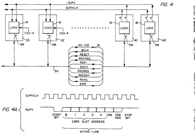
As seen in FIG. 4, the controller bus 50 is made up of the following signal lines:
On the line BCLK, a 4 MHz clock signal is applied by the bus controller 40 to synchronize all operations on the bus. All transitions of other bus signals are in syn-chronization with the positive edges of the BCLK sig-nal.
The lines XO through X15 represent sixteen bit bidi-rectional data, address and control bus lines. These lines are active-high except when they are used as bus re-quest lines, in which case they appear active-low.
The RESET line carries a reset signal generated by the bus controller 40 under control of the MMI proces-sor 35 to initialize the bus interface logic on all devices and to force all devices to the receive mode at that time. The PRSREQ line carries a "present request" signal generated by the bus controller 40. While the PRSREQ line is active (low), each device desiring access to the bus presents a low level on the single XO through XIS line to which it is connected. The number of the X line to which a device's bus request signal is connected corresponds to the physical address of that device on the controller bus 50.
Two ready lines RDYI and RDY2 are provided in the bus 50 to carry "ready" signals generated by the device accessed during a bus operation to indicate that it is presenting valid data (read) or has accepted pres-ented data (write). If the operation is of a type which requires indication of ready, the bus controller 40 moni-tors the RDY lines and terminates a bus operation if both have not been activated (low level) within a prede-termined time after the operation was initiated. Two ready lines are used so that two random access memo-ries 30 and 30' which have been assigned the same logi-cal address may operate in a "shadow write" mode where both memories store the same data during a write operation. The two ready Jines provide the basis for the two memory circuits to independently indicate the "ready" condition under those circumstances where they are operating on inherently-different internal cycle times or where one of these memory circuits may be refreshing when the write operation occurs thus requir-ing more time than the other memory circuit. In either case, the write operation cannot be terminated until both memory circuits have taken the data being pres-ented.
4,442,502
10
9
The PRIGNT line is a priority bus grant line carrying a signal generated by the bus controller 40 to the device requesting priority access. Use of the PRIREQ and PRIGNT lines allow bus access to immediately follow a bus operation in process without expending the bus 5 request/grant time following the current operation.
The PHYS line indicates a physical address being carried by the bus as opposed to a logical address. Only the bus controller 40 is capable of driving this line so that except for the MMI processor 35 operating via the 10
bus controller 40, no other processor device connected to the controller bus 50 can indicate use of physical addressing by taking this line to the active state (low level).
The ERR line in the controller bus SO indicates that 15
an uncorrectable read error in one of the random access memory circuits 30 has occurred during a given read operation. The memory circuit 30 forming the read operation during that operation should take this line low if the uncorrectable error is detected. The ERR line 20 is activated during the bus cycle in which the ROY lines are activated, and the bus operation terminates after the ready cycle in the normal fashion as though the error did not occur. It is the responsibility of the access-ing processor or device and the MMI processor 35 to 25 take action on this error.
The CSO through CS4 lines in the bus 50 provide the physical address to each of the devices connected to the bus. Some or all of these signals are grounded in a pat-tern unique to each card slot and thereby form a five bit 30
physical address. Each device compares this value with the card slot address information used in the physical address mode, a 0 being represented by a grounded pin and a 1 being represented by an open pin, for example.
As seen in FIG. 4, in addition to the lines of the con- 35
troller bus 50 interconnecting the various devices in the controller 16, a pair of special lines SUPV and SUPVCLK extend from each bus controller 40 to each of the devices connected to the controller bus 50. The line SUPV is a serial data line common to all card slots, 40 and carries both address and control information to the devices connected to the controller bus 50 for purposes of controlling connection of those devices or disconnec-tion thereof with respect to the lines of the controller bus 50. This communication line is used exclusively by 45 the MMI processor 35 to control the connect relays 137 which serve to connect to disconnect each of the de-vices to the controller bus SO. The data bits carried by the line SUPV are synchronous with positive transitions of the clock signal carried by the line SUPVCLK. As SO
seen in FIG. 4A, the character format of the serial data on the line SUPV includes one start bit, five card slot address bits, a connect/disconnect bit, one odd parity bit covering the address and connect bits and a stop bit. If the connect bit is a "1" (low level) a connect com- 55 mand is indicated; whereas, if the connect bit is a "0" a disconnect command is indicated.
While various known arbitration schemes are possible for providing access to the controller bus 50 by the various devices associated therewith, the following 60 contention arbitration scheme may be utilized in the system described herein by way of example. Sixteen of the card slots on the bus 50 in the controller 16 have a bus request edge connector pin connected to a unique X(n) line in the controller bus 50. For example, the bus 65 request pin on card slot 3 is connected to line X3, the bus request pin on card slot 4 is connected to line X4, and so forth. This connection is in addition to the
nor-mal bus connection of the X lines to the card slot for addressing purposes. Bus request lines are only con-nected to card slots whose address is 0-15.
The bus controller 40 solicits bus requests from de-vices on the bus 50 by taking the PRSREQ line low. During this bus request cycle, each device desiring access to the bus 50 takes its bus request line low, caus-ing a unique X(n) line to go low for each device request-ing access. Since a direct correspondence exists be-tween the physical card slot and the bit position in which the device in that card slot presents its bus. re-quest, the bus controller 40 is able to unambiguously identify which devices are presenting bus requests.
At the end of the request cycle, the bus requests are stored in respective latches by the bus controller 40, and the bus request which was received on the lowest num-ber X line is selected for service during the next bus operation. After that bus operation is complete, the request latch for that device which was serviced is cleared and the bus controller 40 then selects the next lowest numbered X line-remaining, without activating the PRSREQ again. All requests which were received during the first activation or PRSREQ will be serviced in this manner until all request latches have been cleared. The bus controller 40 will then activate PRSREQ again to initiate a new request cycle.
Physical addressing can only be invoked by the MMI processor 35/bus controller 40 and is used for bus con-trol and diagnostic purposes. This addesss mode is in-voked by the bus controller 40 by activating the PHYS line, subsequent to which all devices connected to the controller bus 50 are automatically placed in the receive mode and interpret address information contained on the XO-X15 lines as a physical (card slot) address.
The use of the PRIREQ/PRIG NT lines of the bus 50 provides even faster bus access for a device with urgent, nondeferable bus requirements. The priority device uses the PRIREQ line as its bus request line instead of one of the X lines as do other devices. If the PRIREQ line is activated during a normal bus request cycle, the bus controller 40 gives the device priority over other de-vices and returns PRIGNT during the next cycle and does not activate the PHYS line as it normally would do for a grant cycle. Since PHYS is inactive, other devices do not interpret the priority grant cycle as a normal grant cycle; instead, while the PRIGNT is low, the priority device places its function and address informa-tion on the bus 50. Thus, the normal arbitrated bus grant cycle is deleted from the priority device's bus access.
Since the controller bus 50 is not used for request/-grant by the priority device, it can request bus access during a bus operation in process by activating the PRIREQ line. The bus controller 40 returns PRIGNT in the first bus cycle following completion of the cur-rent bus operation and the priority device presents its function and address information upon receipt of PRIGNT. In this case, both the normal request and grant cycles have been eliminated.
11
4,442,502
as part of a standard diagnostic program and errors and other faults are also signalled from the individual de-vices to the MMI processor 35 via the ERR line of the controller bus 50. When failure of any device connected to the controller bus 50 occurs and is detected at the 5 MMI processor 35, a procedure is automatically initi-ated for disconnection of that failed device from the controller bus 50 and for connection of the redundant device to the controller bus 50 in the place of the failed unit. This is generally accomplished as seen in FIG. 4 10 using the SUPV and SUPVCLK lines which uniquely extend from the bus controllers 40 to the other devices of the controller 16, which devices are selectively con-nectable to the controller bus 50 by way of individual switches SW located between the bus 50 and the edge 15 connectors for the device circuit cards. Bus disconnect logic circuitry 18 associated with each of these devices responds to the physical address of the devices as indi-cated at the time the device card is plugged into the controller bus 50 via lines CSO-CS4 and the serial data 20 received from the controller 40 via the line SUPV in synchronism with the clock signals applied to the line SUPVCLK.
As an example, FIG. 4 shows a system processor 25
and a bus controller 40 connected by way of switches 25 SW to the controller bus 50. In addition, a redundant system processor 25' is also available for connection to the bus 50 via its switch SW. At any time a fault is detected in the system processor 25 by the MMI proces-sor 35, the bus controller 40 applies to the SUPV line 30 the physical address of the processor 25 along with a disconnect command as serial data in the format shown in FIG. 4A causing logic 18 in the processor 25 to re-lease the switch SW. Also, the physical address of the redundant processor 25' along with a connect command 35 is applied to line SUPV by the bus controller 40 to effect connection of the redundant processor 25' to the bus 50 in a similar way. This occurs automatically within the controller 16, resulting in fault correction without having to wait for outside maintenance. As 40 seen in FIG. 4, even a redundant bus controller 40' is provided in the controller 16 for connection to the bus 50 by the MMI processor when failure of the bus con-troller 40 occurs.
In this way, redundancy is accomplished by inclusion 45 in the controller 16 of one or more extra devices which can be dynamically switched into service when one of the active units malfunctions. Since all devices of a particular type are identical, it is not necessary to pro-vide redundancy on a one-for-one basis, thereby mini- 50 mizing the cost of provision of redundant elements within the system. In addition, when the spare device is switched into service, it is assigned the same logical address as the unit which failed, so that no program changes are required and the operation of the controller 55 resumes exactly as before the failure occurred.
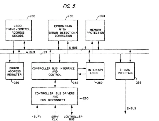
Depending on system size and feature content, one or more system processors 25 are included in the control-ler 16 of each remote switching unit 12. The system processor may take the form of a Zilog Z800 I single 60 chip 16 bit microcomputer. A general block diagram of the system processor 25 showing the basic elements thereof is seen in FIG. 5. The microprocessor 250 in-cludes, in addition to a Z8001 chip, a crystal oscillator which provides for operation of the processor system at 65 a 4 MHz rate. The processor chip 250 connects to the other elements of the processor via a 23 bit address (A) bus and a 16 bit bidirectional data (D) bus.
12
The local memory 252 associated with each system processor 25 includes both EPROM and dynamic RAM storage. Each word location of RAM and EPROM actually contains an additional 6 bit Hamming code for single or double bit error detection and single bit error correction, and the write byte operation is implemented via a word read-modify-write cycle so that the Ham-ming bits can reflect the proper code for the new word as a whole unit. In combination with this feature, the local memory 252 includes memory error detection and correction logic capable of providing single error cor-rection of 16 bit data from RAM and EPROM memory for all read operations. This logic generates the six Hamming bits prior to a write operation for loading into the 22 bit wide RAM. Each read access to the proces-sors local RAM memory is checked by the error detec-tion and correcdetec-tion logic, and if a correctable error occurs, the logic provides the processor chip 250 with corrected data and automatically writes the corrected data back to memory. Each time such error correction occurs, a local corrected read error latch is set, which latch can be observed by the MMI processor 35 using a diagnostic read operation and can be reset only by that processor during a diagnostic write operation. On the other hand, if an uncorrectable read error is detected, the address is saved in an error address register 256, a non-maskable interrupt is generated to the processor chip 250 and a processor fault latch is set which can be observed by the MMI processor 35 in a similar manner to correctable errors. The memory error detection and correction logic, which has not been described or illus-trated in detail herein, can take any known form of error detection circuitry depending upon the types of errors to be detected. For purposes of the present invention, it is sufficient to understand that error detection is pro-vided within each system processor and other elements of the controller 16, which errors can be monitored by the MMI processor 35 as part of the diagnostic and control features of the present invention.
The memory protection circuit 254 serves to protect the more common data stored in various areas of the local memory 252 from unauthorized use. In this re-gard, the circuit 254 is provided in the form of a high speed RAM which stores memory protection bits asso-ciated with blocks of words in the local memory 252.
During each memory access, the type of operation to be performed is compared against the protection bits pre-viously loaded for that area of memory, and if a viola-tion is detected, a non-maskable interrupt is generated to the processor chip 250 indicating the attempt at unau-thorized access to the data.
The controller bus interface and control circuit 258
provides the various registers and control logic for sending or receiving data to and from the various ele-ments of the system processor 25 to the controller bus
4,442,502
13
the switching in and out of redundant modules con-nected to the controller bus 50, the controller bus inter-face and control circuit 258 also provides the logic necessary to the physical-to-logical transformation of addresses as determined via the logical address loaded 5 by the MMI processor 35 by way of the controller bus SO.
An example of the controller bus drivers and receiv-ers and bus disconnect circuit 260 is seen in FIG. SB. At the time a device card is plugged into the controller bus 10 SO, the card slot address as provided on lines AO through A4 provide a physical address for the device which corresponds to the card slot position along the controller bus SO and is used by the MMI processor 35 for physical addressing of the devices on the controller 15 bus SO. At the time a bus connect disconnect command is to be forwarded to one of the devices, a signal is applied to the SUPV line from the bus controller 40, having a format such as shown in FIG. 4A. This serial data is applied in common to a data register 115 in each 20 device in synchronism with the clock signal received in line SUPVCLK. The parity bit, five bit address and the connect/disconnect command bit are applied from the data register 115 to a parity check circuit 120 to deter-mine that the serial data has been correctly received. 25 When parity is confirmed by the circuit 120, an enable signal is applied to a comparator 125 which receives the address bits stored in the data register 115 at one of its sets of inputs and the physical address of the device at its second set of inputs. Comparison between these two 30 addresses indicates that the serial data is designated for that particular device as indicated by an output from the comparator 125 to a pair of AND gates 130 and 131, the AND gate 130 also receiving the connect/disconnect command bit from register 115 and the AND gate 131 35 also receiving this same command bit via an inverting gate 132. If the command bit stored in the register 115 represents a connect command, the gate 130 will be enabled to set a connect flip-flop 135. On the other hand, if the command bit in the register 115 represents 40 a disconnect command, the gate 131 will be enabled to reset the flip-flop 135. Thus, depending upon the state of the connect flip-flop 135, the switch which connects the device at the edge connector to the conductors of the controller bus SO is either enabled or released. 45
14
ration and diagnostic functions. Via its dedicated con-nection through the Z bus to the bus controller 40, the processor 35 has unique access to controller bus status and control functions as well as interface to external maintenance and diagnostic features.
In addition to the bus arbitration logic and timing control functions, the bus controller 40 comprises a collection of I/O devices which can be locally accessed by the MMI processor 35 via the Z bus connection. These separate I/O devices are provided generally in the form of a number of Intel 8259 interrupt controller chips along with Intel 8253 programmable interval timer chip to effect timing operations and Intel 8251 programmable communications interface chips to pro-vide for transmission and reception of serial asynchro-nous data and control/status information.
The modem 55 is provided in the form of a full duplex 1200 bit per second modem and a FCC part-68 regis-tered interface to a central office trunk to provide ac-cess to a remote diagnostic center for reporting of sys-tem status and execution of remotely-provided diagnos-tics. Thus, when a failure is detected in anyone of the devices connected to the controller bus 50, in addition to the disconnection of the device from the bus SO and the connection of a redundant device in its place, the MMI processor 35 automatically initiates communica-tion to the remote diagnostic center via the modem 55 indicating the serial number, type of module, problem and location of the system. Thus, service personnel can immediately respond to the failure indication, effecting a replacement of the failed device at the earliest-possible time. However, it is of extreme importance to note that the system operation continues in spite of the failure of the device in the controller 16 in view of the automatic switching of a redundant device in place of the failed unit, so that no interruption to system operation occurs, nor does the system need to wait for service personnel to replace the failed unit before operation can continue. The control panel 60 provides a control and display capability for service personnel within the system. Con-trol is provided via a keypad and a group of unique function keys in combination with an alphanumeric display to indicate diagnostic results and system status. The interface from the control panel 60 to the MMI processor 35 is effected via the bus controller 40.
The second major portion of the remote switching unit 12 is the terminal portion which includes the ISL interfaces 70, the matrix 85 and the expanders 75, all of which are interconnected by the terminal bus 65 and the transmit and receive PCM buses 66 and 67. The matrix 85 which provides the data switching in the remote switching unit 12 may be a standard single stage non-blocking time slot interchange switch capable of 512 The random access memory 30 in the controller 16
provides for storage of the data base for the system processors 25 as well as temporary call processing data, and is designed to accommodate 16K, 32K, or 64K bit dynamic RAM chips. Like the other devices in the 50 controller 16, the RAM 30 also includes error detection and correction logic of the type described in conjunc-tion with the system processor 25 for detecting errors and identifying such errors and other malfunctions to
the MMI processor 35. 55 simultaneous connections, i.e., 512 inputs and 512 out-puts. In a preferred embodiment of the invention, 384 of the input/output links through the matrix 85 are used for connection to the ports via the expanders 75 and The bus controller 40 provides the timing, arbitration
and control logic necessary for operation of the control-ler bus SO. Requests for bus access from processors 25 and other devices connected to the bus 50 are solicited, arbitrated and granted by this device on a first-come, 60
first-served basis. Bus timing errors and device data errors are detected by the bus controller 40 and relayed to the MMI processor 35 via the interface 255 the Z bus connection in the processor (see FIG. 5), which repre-sents a direct noncontroller bus control/status/data 65 path to the MMI processor 35. MMI processor 35 is basically identical in every respect to the system proces-sor 25, but is dedicated to system initialization,
configu-port interface circuits 80. The remaining 128 links are available for connection to the interswitch links 14, providing for connection to terminals in other remote switching units 12 via the central switching unit 10.