2018 3rd International Conference on Information Technology and Industrial Automation (ICITIA 2018) ISBN: 978-1-60595-607-7
Modular Hardware Implementation of SOM
Neural Network Based on FPGA
Qing Shao, Lin Du and Lianming Wang
ABSTRACT
With the development of artificial intelligence technology, artificial neural networks have been widely used in many fields. And traditional artificial neural network implementation methods generally have the disadvantages of poor flexibility and low real-time performance. To solve these problems, this paper presents a modular hardware implementation method of SOM neural network based on FPGA. Firstly, based on the analysis of the model structure, operation process and learning algorithm of SOM neural network, combined with the conditions and limitations of FPGA hardware implementation, the network model is divided into five modules with relatively independent structure and function. Secondly, VHDL is used to describe the RTL of each module to build a common module library. Finally, in practical applications, the target hardware of the SOM neural network can be constructed by combining the modules according to requirements. When building a hardware network, flexible configuration of the arithmetic structure is achieved by setting and passing parameters. The performance test results show that compared with the software simulation method and the traditional hardware implementation method, this method has higher running speed and more flexible operation structure, and can meet the application requirements of high-speed and miniaturized intelligent information processing system.1
INTRODUCTION
At present, with the development of artificial intelligence technology, the application of artificial neural network is more and more extensive, and people have higher and higher requirements for computing power. The traditional artificial
1
neural network is mainly implemented by software simulation. Due to the limitation of the computing structure of the general-purpose computer, the advantages of parallel computing of the neural network cannot be fully utilized, resulting in poor real-time performance. Therefore, the hardware implementation of artificial neural networks has gradually become a research hotspot. Among the research results of many hardware implementations, the VLSI implementation method is considered to be the best way to realize the neural network because of its more mature technology, high precision and strong anti-noise ability[1-2].
The implementation method based on VLSI can be divided into analog implementation, digital implementation and digital-analog hybrid implementation. Compared with the other two methods, digital circuits are easier to achieve modularization, scalability, anti-interference ability, and many EDA tools support them [3]. As a semi-custom digital design carrier, FPGA has the characteristics of rich logic resources, flexible configuration, short development cycle and parallel computing. It is widely used in neural network hardware implementation research[4].
[image:2.612.165.464.444.655.2]At present, the research results of artificial neural network based on FPGA are mostly oriented to specific application scenarios, and the internal computing structure cannot be set according to requirements, and it is not universal [5-6]. Therefore, there is an urgent need for an artificial neural network hardware implementation method in which an internal computing structure can be configured on demand, capable of speed and resource optimization, and modularization. This paper intends to develop this method for SOM neural networks.
SOM NEURALNETWORK
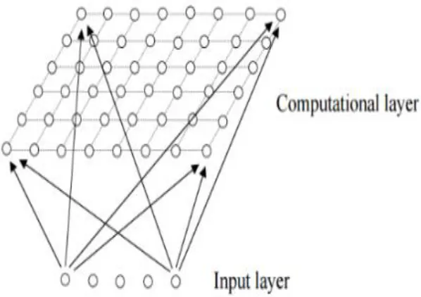
SOM neural network is a two-layer feed forward fully connected network composed of input layer and output layer. The role of the input layer is to pass external input to the output layer. The output layer is also called the competition layer, and the arrangement of the competition layer neurons has various forms, such as a one-dimensional line array, a two-dimensional plane array, and a three-dimensional grid array. As shown in Figure 1, two-three-dimensional planar array organization is the most typical organization of SOM networks. Each of the competing neurons is connected to all the neurons in the input layer, and the connection strength is large or small, which is represented by the network weight [7].
SOM neural network adopts unsupervised self-learning algorithm, and has no expected output signal to guide the learning of the network. The network only adjusts the weights of the network through its own structure and learning rules, so that each competing neuron can only excite specific input.
MODULEDIVISIONANDIMPLEMENTATION
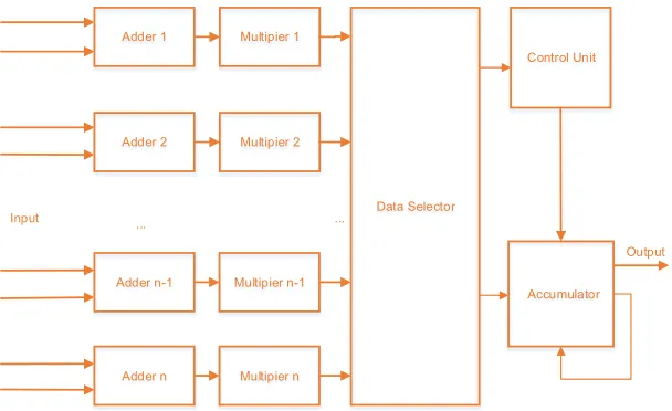
According to the above principle of the SOM neural network, the SOM neural network is divided into five modules, namely, a learning module, a data processing module, a distance calculation module, a winning neuron calculation module, and a display module, as shown in Figure 2. The hardware implementation of each module is performed separately, and then the five modules are properly combined to implement the target hardware SOM neural network. Since the distance calculation module is the most important part of the SOM network hardware implementation process, the following mainly introduces the implementation idea of this module.
The distance calculation module can adjust the degree of parallelism of the network operation structure according to the general parameters, and calculate the Euclidean distance between the input and each competing neuron.
Because the square root operation consumes a lot of logic resources when calculating the Euclidean distance, we are committed to doing these operations with as little logic resources and runtime as possible. Therefore, we simplify the original Euclidean distance formula, and omit the square operation in the Euclidean distance formula; at the same time, the subtraction of two numbers can be seen as the addition of the opposite number of one number and another number; and the square operation can be seen as the multiplication operation of two identical numbers. At this point, the distance calculation formula involves only addition, multiplication and accumulation operations. Finally, the Euclidean distance formula is simplified as formula (1).
2 2
1 1
,j [ ( ij )] [ n ( ijn)]
i x w x w
Learning Module Distance Calculation Module
Data Processing
Module Display Module
Winning Neuron Calculation Module
Input
[image:4.612.110.489.84.179.2]Output
Figure 2. Module division of SOM neural network hardware implementation.
Adder 1
Adder 2
Adder n-1
Adder n
Multipier 1
Multipier 2
Multipier n-1
Multipier n
Data Selector
Control Unit
Accumulator Output ...
... Input
Figure 3. The block diagram of the distance calculation module.
At the same time, we find that there is no necessary connection between the input and the process of summing the corresponding weights for the same input vector. Then, we can set this process to a variable-level parallel computing structure in the FPGA, and also set the degree of parallelism through common parameters.
[image:4.612.150.454.225.411.2]EXPERIMENTALRESULT
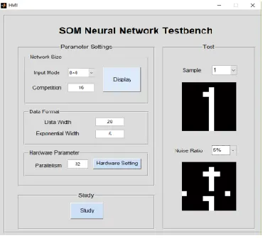
[image:5.612.199.397.272.440.2]To verify the functionality and performance of the designed hardware SOM neural network, the network was used for binary image recognition with a resolution of 8 * 8 containing noise from 0 to 9. The FPGA used in this article is the EP4CE115F29C7 of the Cyclone IV E series from Altera Corporation (Intel PSG) with a total of 114480 LEs of logic resources. Secondly, a graphical user interface is developed in the PC side by means of MATLAB 2012a 64-bit, and the parameter setting and learning process are completed through the graphical user interface. FPGA development board and PC terminal MATLAB graphical user interface are shown in Figure 4 and Figure 5 respectively.
Figure 4. FPGA development board.
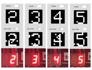
[image:5.612.206.391.489.657.2]As shown in Figure 6, the original binary images 2, 3, 4, and 5 are identified by adding a 5% noise ratio. The first line in Figure 5 is the original binary image, the second line is the binary image with noise added, and the third line is the recognition result of the SOM hardware network. From the recognition results of Figure 6, it can be seen that the SOM hardware network system can correctly realize the binary image recognition with noise, which proves the correctness of the modular design method in this paper.
The performance test is to test the network speed and area occupancy by configuring the hardware network into different computing structures, and at the same time, compare it with MATLAB software simulation. The hardware SOM network in FPGA has a clock frequency of 50MHz, and the software simulation environment is: Intel i5-6600 quad-core processor, 8GB DDR4 memory, Windows 10 Professional 64-bit, MATLAB 2012a 64-bit, etc.
Using 0-9 binary images with 8*8 resolution and 5% noise ratio as test samples, 64 neurons in the input layer and 16 neurons in the competitive layer were detected. The adders and multipliers in hardware SOM neural network are set to different numbers, and their logical resource occupation and network running time are observed. At the same time, it is time-consuming to test the MATLAB software simulation, and then compare with the former. The performance test results are shown in TABLEI.
[image:6.612.221.373.380.496.2]Figure 6. Identification results.
TABLE I. THE PERFORMANCE TEST RESULTS.
Speed and area for different computing structures
Adders 64 32 1
Multipliers 64 32 1
Area occupancy 53% 27% 2%
Latency(FPGA) 0.25ms 0.48ms 15.91ms
It can be seen from TABLEI that when the network scale is fixed, as the adder and multiplier in the distance computing structure increase, the hardware SOM network will run faster, but the logical resource occupancy will also increase. Therefore, in practical applications, it is necessary to balance the speed and area. When the number of adders and multipliers is 64, its speed is nearly 7 times faster than software simulation. At the same time, by properly increasing the number of adders and multipliers, the running speed of hardware network can also exceed that of software simulation.
CONCLUSIONS
This paper presents a modular hardware implementation method of SOM neural network based on FPGA. The test results show that this method can achieve optimal design of running speed and resource occupancy. Compared with the software implementation method and the traditional hardware implementation method, this method has faster running speed and more flexible operation structure, and can meet the application requirements of high-speed and miniaturized intelligent information processing system. This paper also has reference to the hardware implementation of other types of artificial neural networks.
REFERENCES
1. Graf, H. P., Jackel, L. D., & Hubbard, W. E. (1988). Vlsi Implementation of a Neural Network Model. Computer, 21(3), 41-49.
2. Ruping, S., Porrmann, M., & Ruckert, U. (1998). Som Accelerator System. Neuro Computing, 21(1–3), 31-50.
3. Mailachalam, B., & Srikanthan, T. (2002). Area–Time Issues in the Vlsi Implementation of Self Organizing Map Neural Networks. Microprocessors & Microsystems, 26(9), 399-406.
4. Granado, J. M. (2007). Using FPGAs to Implement Artificial Neural Networks. IEEE International Conference on Electronics. IEEE.
5. Kurdthongmee, W. (2008). A Novel Hardware-Oriented Kohonen Som Image Compression Algorithm and its Fpga Implementation. Journal of Systems Architecture, 54(10), 983-994. 6. Miguel, P., & Alastair, A. (2009). A Hybrid System for Embedded Machine Vision Using Fpgas
and Neural Networks. Machine Vision & Applications, 20(6), 379-394.