Analysis and Design of High Performance Ring Voltage
Controlled Oscillator
Ashraf Mohamed Ali Hassen
Department of Electronics and Communications
Modern Academy in Maadi
ABSTRACT
The voltage controlled oscillator (VCO) may be considered one of the most important building blocks in modern communication applications such as microprocessor clock generation, wired and wireless communications, system synchronization, and frequency synthesis. The search in the field of design for high performance VCOs has been increasingly more important and becomes an active research area. In the past decade, The Researches on VCOs have been based on the areas of higher frequency, lower phase noise, low power, low operating voltage, and increased tuning range. However many of these objectives can be only achieved at the expense of some other objectives. This thesis analyzes the design of high performance ring VCOs. The beginning of the thesis is reviewing the basic ring VCOs. The different designs are also introduced. Finally, the circuit techniques used in a proposed VCO based on the new technique is designed and simulated in 65nm CMOS SOI process. The results of proposed device are compared and confirmed the usability of the new ring VCO cell topology. Finally, a conclusion of the proposed design of high performance ring VCOs is explained.
General Terms
Voltage Controlled oscillator - Clock Generation - Wireless Communications.
Keywords
Phase noise, power, operating voltage, tuning range
1.
INTRODUCTION
A VCO is the most important basic building blocks in analog and digital circuits [1]. There are various implementations of VCOs. One of them is a ring oscillator based on VCO, which is commonly used in the clock generation subsystem. The main reason of using ring oscillator in different fields of communications system is a direct consequence of its easy integration. Due to their integrated nature, ring oscillators have become one of the most important building block in many digital and communication systems. The most applications of voltage controlled oscillators are recovery circuits for serial data communications [1,2] disk-drive read channels [3] on-chip clock distribution [4], and integrated frequency synthesizers [5,6].There are many tradeoffs in the design of a ring oscillator in terms of speed, power, area, and application domain [7]. The problem of designing a ring oscillator is the focus of interest in this paper. In the communication system, the voltage controlled oscillator is the important component, especially in the PLL circuit, clock recovery circuit and frequency integrated circuit, so it is the top priorities [8].
Over the last several decades, the rapid growth of commercial communication applications has led to a commensurate
demand for better and cheaper devices. While Moore’s law has continued its course mostly undisturbed for close to a half century, digital circuits have experienced continuing improvements due to a doubling of available transistors every two years [9,10]. Such rapid technology developments revolutionized digital electronics, there by fueling one of the fastest growing markets ever observed.
Analog circuits have also controlled from technology scaling, although at a slower pace due to the many challenges in adapting to degrading device characteristics. Because of the continuing reduction of voltage headroom and intrinsic device gain, high precision analog building blocks have had to adopt higher degrees of design complexity.
2.
THE DIFFERENTIAL AND
SINGLE-ENDED VCOs
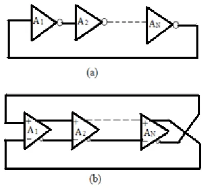
[image:1.595.341.540.539.725.2]A ring oscillator consists of a number of delay stages, with the output of the last stage fed back to the input of the first. To achieve oscillation, the ring must provide two conditions which are summarized as follow. A phase shift of 2π and a unity voltage gain at the oscillation frequency. Each delay stage must introduce a phase shift of π=N, where N is the number of delay stages. The remaining phase shift is introduced by a dc inversion [11]. This means that for an oscillator with single-ended delay stages, an odd number of stages are an important condition for the dc inversion. In case of using differential delay stages, the ring can have an even number of stages and that case is happened when the feedback lines are swapped [12]. The topology of the two circuits is shown in Figure 1.
Fig. 1: Ring oscillator types: (a) single-ended
one of the simplest way to control the charge and discharge time of an inverter is to control the flow of the current through the inverter, via a voltage controlled current source, as shown in Figure 2. This current source is driven by the control voltage, Vctrl, and the current will determine the charge up and discharge time of the inverter. This topology is called current-starved inverter, as the regular inverter is short of the current they are normally allowed to consume.
Fig. 2: The current-starved inverter
Differential VCO cells have better oscillation than the singled ended versions and noise performance, due to their current mode logic and native differential noise rejection. In theory, the minimum number of stages required for oscillation of differential cell design is two, as the outputs of the second cell can be crossed to get additional 90° phase shift. This circuit is shown in figure 3
Fig. 3: The Differential VCO with resistive load
3.
THE RING VCO
It should begin by giving a brief for the advantages of both differential and single-ended topologies. First, differential topology has fast oscillation frequency due to its current mode logic, on the other hand, the output of the differential topology drives only one gate, whiles the output in the singled-ended case, drives both the gates of an NFET and a PFET. This indicates that the output drives as less capacitance as possible to achieve maximum speed.
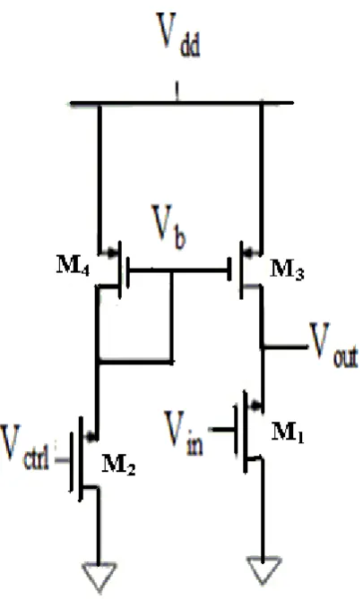
[image:2.595.336.539.307.642.2]Second, the current source in the differential design has no major effect on the tuning range, as long as there is a voltage controlled load device, which controls the gain, while the current source in the singled-ended design is important because it is considered the only tuning mechanism [13]. In case of removing the current source and having a voltage controlled load device, this helps in boosting the output swing while maintain the tuning range. This idea is shown through a VCO cell which is shown in figure 4
Fig. 4: The Ring VCO Cell Topology
[image:2.595.63.278.490.734.2]design which are as follow the DC offset problem and small swing at low control voltage problem.
4. THE MODIFIED RING VCO
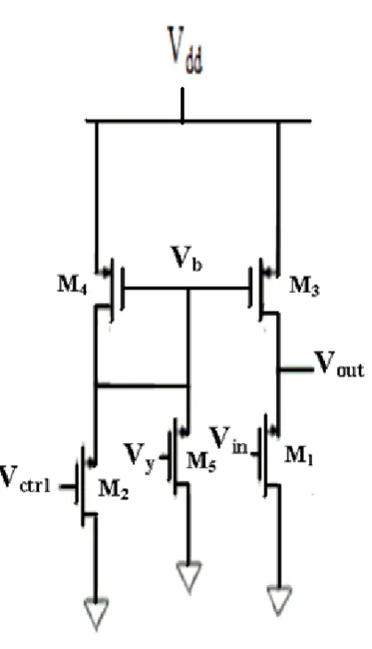
The VCO output swing is minimized as control voltage goes close to zero. This is due to the fact that as Vctrl goes near zero, the voltage at node Vb becomes close to VDD. This will put the PFET load into subthreshold region. Though this circuit will still oscillate, but the output swing will be extremely small and cannot drive any outputs. As a result, the VCO does not work at low control voltages. To let the VCO to oscillate at low control voltage, This can be achieved by adding an extra diode connected NFET to the bias circuit, as shown in Figure 5. This diode connected NFET serves as a feedback device that lets the current passes through it whenever the voltage at node Vb becomes too high. NFET device can be sized as much smaller compared to the main NFET so that it has little effect when the control voltage is high.
[image:3.595.332.540.150.361.2]Fig.5: The Modified Ring VCO
5.
The PROPOSED RING VCO
The proposed circuit shown in figure 6 is based on the benefits of the previous of the two circuits discussed in
[image:3.595.71.281.302.668.2]sections 3 and 4. In the proposed circuit, M3 and M4 is not connected directly to vdd as the pervious circuit. But it is connected to PMOS transistors (M6 and M7) instead. This connection helps us to obtain large tuning range as the two PMOS transistors decrease the voltage of Vdd before it connects to transistors M3 and M4. This connection also helps in obtaining acceptable phase noise.
Fig.6: The proposed circuit
6.
ANALYSIS OF
THE PROPOSED
CIRCUIT
The proposed circuit is analyzed through the complete circuit shown in figure 7
[image:3.595.321.540.469.733.2]With no gate resistance, the voltage on the capacitor Cin is equal to Vout (t). However, with the gate resistance, the voltage on Cin no longer equals Vout (t), and time that the voltage crosses the mid-swing point will shift slightly. This is important because it affects the limits of integration when integrating the current. Therefore, the time that the voltage at Cin crosses the mid-swing point, Vsw/2, must be determined. This is done by solving (1) for t 0.
𝑣
𝑜𝑢𝑡𝑡
0− 𝐼
𝐶𝑖𝑛𝑡
0𝑅
𝑔= 𝑣
𝐷𝐷−
𝑣
𝑠𝑤2
(1)
Where Icing(t) is found through KCL. To simplify the expressions, all the parasitic capacitances will be lumped into a term called Cpar . Making the substitutions into (1) gives (2).
sin(𝜋2𝑓𝑡𝑜𝑁 − 𝑁 − 1
𝑁 ) + 2𝜋𝑓𝑅𝑔𝐶𝑝𝑎𝑟cos(𝜋
2𝑓𝑡0𝑁 − 𝑁 − 1
𝑁 )
= 𝑂 (2)
Solving (2) for t0 gives (3).
𝑡0=
𝜋𝑁 + 𝜋 − 𝑎 tan 2𝜋𝑓. 𝑅𝑔𝐶𝑝𝑎𝑟 𝑁
2𝜋𝑓𝑁 (3)
The argument of atan( 2fRgCpar) is much less than 1. If is small, then tan() ≈ . Therefore (3) can be simplified to (4)
𝑡0=
𝜋𝑁 + 𝜋 − 2𝜋𝑓. 𝑅𝑔𝐶𝑝𝑎𝑟𝑁
2𝜋𝑓𝑁 (4)
Eq. (4) can be further reduced to (5), which gives the time that the voltage on Cin crosses the mid swing point. This is the time to be used as the lower limit on the integration of the current.
𝑡𝑜=𝑁 + 12𝑁𝑓 − 𝑅𝑔𝐶𝑝𝑎𝑟 (5)
The subsequent times to be used in the integration are still separated by a quarter period. Using the new integration limits. After substitution and integration, (6) is obtained.
1
2𝐶𝑖𝑛 =
𝜋 + 2 + 4𝜋𝑓1𝑅𝑃𝐶𝑝𝑎𝑟
8𝜋𝑓1𝑅𝑝
+ 4 − 8𝜋𝑓1𝑅𝑝𝐶𝑝𝑎𝑟 sin 𝜃 cos 𝜃
8𝜋𝑓1𝑅𝑝
− 4 + 8𝜋𝑓1𝑅𝑝𝐶𝑝𝑎𝑟 𝑐𝑜𝑠2(𝜃)
8𝜋𝑓1𝑅𝑝 (6)
where =fRgCpar and Rp is the equivalent resistance of the PMOS load. Since <<1, sin() is << 1, and these terms become negligible. Also, since <<1, cos() ≈ 1. Making these substitutions results in (7)
1
2𝐶𝑖𝑛=
𝜋 + 2 + 4𝜋𝑓1𝑅𝑝𝐶𝑝𝑎𝑟
8𝜋𝑓1𝑅𝑝
−(4 + 8𝜋𝑓1𝑅𝑝𝐶𝑝𝑎𝑟
8𝜋𝑓1𝑅𝑝 (7)
Solving (7) for f1 gives
𝑓1=
𝜋 − 2
4𝜋𝑅𝑝(𝐶𝑖𝑛+ 𝐶𝑝𝑎𝑟) (8)
The same steps can be repeated to determine f2. The result is given in (9).
𝑓2=
4𝜋𝐼𝑠𝑠𝑅𝑝+ 𝑁𝑉𝑠𝑤(2 − 𝜋)
4𝜋𝑁(𝑉𝑠𝑤 𝐶𝑖𝑛+ 𝐶𝑝𝑎𝑟 + 2𝐼𝑠𝑠𝑅𝑔𝐶𝑝𝑎𝑟)
(9)
Averaging f1 and f2 gives the overall frequency equation
𝑓 = 𝐼𝑠𝑠
2𝑁𝑉𝑠𝑤 𝐶𝑖𝑛+ 𝐶𝑝𝑎𝑟 ×
1 +𝐼𝑠𝑠𝑉𝑁𝑅𝑔
𝑠𝑤 .
𝐶𝑝𝑎𝑟
𝐶𝑖𝑛+ 𝐶𝑝𝑎𝑟(
1 2 −𝜋 )1
1 +2𝐼𝑉𝑠𝑠𝑅𝑔
𝑠𝑤 .
𝐶𝑝𝑎𝑟
𝐶𝑖𝑛+ 𝐶𝑝𝑎𝑟
(10)
Eq. (10) is of the form (1+a)/(1+b) where a,b << 1. Therefore (1+a)/(1+b) ≈ 1-(b-a). Using this simplification (10) reduces to (11)
𝑓 = 𝐼𝑠𝑠
2𝑁𝑉𝑠𝑤 𝐶𝑖𝑛+ 𝐶𝑝𝑎𝑟
×
1 − 𝐼𝑠𝑠𝑅𝑔𝐶𝑃𝑝𝑎𝑟
𝑉𝑠𝑤 𝐶𝑖𝑛+ 𝐶𝑝𝑎𝑟
2 − 𝑁 1
2−
1
𝜋 (11)
7. SIMULATION RESULTS
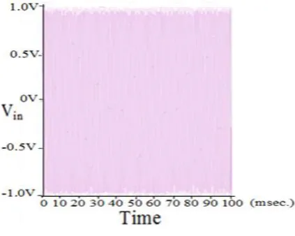
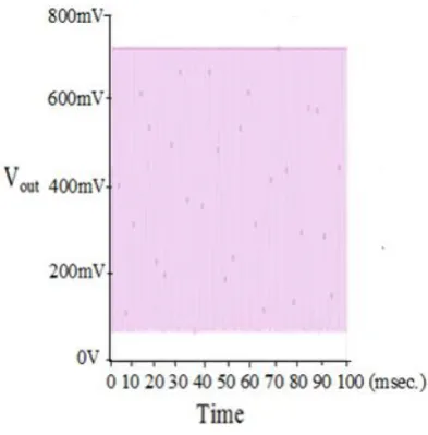
[image:4.595.327.539.559.728.2]The proposed ring vco is simulated via Pspice tool, figure 8 illustrates the input signal in the time domain.
Figure 9 shows the response of the circuit versus the variation of Vctrl
Fig. 9: The response of the circuit versus Vctrl
The conclusion from figure 9 is that Vout varies from .6v to 1v. This increases the tuning range as Vout Varies linearly with it. This is the good benefit obtained from the proposed circuit. Figure 10 study the oscillation of the proposed circuit in the time domain
Fig. 10: The response of the proposed circuit in time domain
8. COMPARISON OF THE RESULTS
Table 1 demonstrates the comparison of the different researches in ring vco approaches to illustrate the benefits of the proposed work.
Table 1. Comparison between different approaches
Technology Frequency Power supply
Phase noise This work 65nm SOI
CMOS
2.5~36.6 GHz
1v -95.5
dBc/Hz
Ring VCO
65nm SOI CMOS
3.2~26.3 GHz
1.5v -97
dBc/Hz
Modified Ring VCO
65nm SOI CMOS
2.8~28.5 GHz
1.5v -96.5
dBc/Hz
9.
CONCLUSIONS
VCO is the one of the most important building block in modern communication systems. This paper analyzed the design of high performance ring VCO. Through simulation, great results from the proposed design were obtained. The proposed design of ring VCO was concentrated from maximum oscillation frequency and tuning range perspective. Also the Proposed design achieved a large tuning range with acceptable phase noise and low operating voltage which are good results in the domain of search. This work had positive effect on the study and application of the voltage controlled oscillation in the wireless communication systems.
REFERENCES
[1] C. H. PARK, O. KIM, B. KIM 2001, "A 1.8-GHz self-calibrated phase locked loop with preciseI/Q matching", IEEE J. Solid-State Circuits, vol. 36, pp.777-783. [2] L. SUN AND T. A. KWASNIEWSKI 2011, "A 1.25-GHz
0.35- m monolithic CMOS PLL based on a multiphase ring oscillator", IEEE J. Solid-State Circuits, vol. 36, pp.910-916.
[3] J. SAVOJ AND B. RAZAVI 2001, "A 10-Gb/s CMOS clock and data recovery circuit with a half-rate linear phase detector", IEEE J. Solid-State Circuits, vol. 36, , pp.761-767.
[4] C. K. K. YANG, R. FARJAD-RAD, M. A. HOROWITZ, 2008, "A 0.5- m CMOS 4.0-Gbit/s seriallink transceiver with data recovery using oversampling" , IEEE J. Solid-State Circuits, vol. 33, , pp.713-722.
[5]M. ALIOTO, G. PALUMBO 2010, "Oscillation frequency in CML and ESCL ring oscillators", IEEE Trans. Circuits Syst. I, vol. 48, pp.210-214.
[6] B. RAZAVI 2007, "A 2-GHz 1.6-mW phase-locked loop", IEEE J. Solid-State Circuits, vol.32, pp.730-735. [7] G. JOVANOVI C, M. STOJ\CEV, Jun 2007, "A Method
for Improvement Stability of a CMOS Voltage Controlled Ring Oscillators", ICEST, vol. 2, pp. 715-718.
[8] Huang Shizhen , Lin Wei , Wang Yutong ,Zheng Li, March 18 – 20 2009, "Design Of A Voltage-controlled Ring Oscillator", pp.614-620.
[image:5.595.62.259.426.626.2][10] N. M. Nguyen and R. G. Meyer May 2002, "Start-up and Frequency Stability in High- Frequency Oscillators", IEEE Journal of Solid State Circuits, vol. 27, pp. 810-820.
[11] S. Docking, M. Sachdev 2003, "A Method to Derive an Equation for the Oscillation Frequency of a Ring Oscillator", IEEE Trans. on Circuits and Systems - I: Fundamental Theory and Applications, vol. 50, 2, pp.259-264.
[12] G. Jovanovic, M. Stojcev, Z. Stamenkovic, 2010 "A CMOS Voltage Controlled Ring Oscillator with Improved Frequency Stability",vol.2,1, pp.1-9.