Vdd
A Substrate Biased Full Adder Circuit
C. SaravanakumarAsst. Prof – ECE, Department of ECE, Valliammai Engineering College
Abstract— With the recent advances in the VLSI design and technology, the challenge in the design complexity of IC has grown. One of the major challenges is to design logic with power minimization. This is due to two reasons; one is the long battery backup for mobile and portable devices and second is due to increase in number of transistors packed in a single chip which will lead to reliability problems. As addition is one of the indispensible operations in digital system we selected the basic full adder and the substrate biased full adder. The design criterion of a full adder is usually multi – fold. In this paper we did a comparative study based on the number of transistor used. The circuits are simulated in a famous EDA tool ORCAD. The results show that there is a considerable reduction in transistor count with respect to substrate biasing. In future these adders can be developed into an enhanced ALU with added features.
Keywords— CMOS adder, ORCAD, Substrate biased adder, transistor count, XOR Gate.
I. INTRODUCTION
Low speed and high performance are the design trade off in the field of VLSI design. In recent days the performance of a chip can be considered as an analogy for speed. The extensive development in the field of portable systems and cellular networks has intensified the research efforts in low power microelectronics. The low-power design has become a major design consideration. The design criterion of a full adder cell is usually multi-fold. Transistor count is, of course, a primary concern which largely affects the design complexity of many function units such as multiplier and algorithmic logic unit (ALU). This paper makes an effort to design some basic digital circuits with an improved CMOS transistor model [1], supported by mathematical and logical equations. In this paper the basic analysis of CMOS model is described and then used this model to design Full adder circuit. Then it describes the substrate biased CMOS model and using this model the Full adder circuit is designed. Then it concludes the improvement in number of transistor used.
II. CMOSTRANSISTORMODEL
A. CMOS Transistor
A Complementary MOS transistor consists of both nMOS and pMOS devices. The gate terminal of an nMOS transistor controls the flow of current between the source and drain. When the gate is low, the nMOS transistor is OFF and almost zero current flows from source to drain. A pMOS transistor is just the opposite, being ON when the gate is low and OFF when the gate is high.
B. CMOS Inverter
A basic CMOS inverter is given in Fig.1 along with its truth table. It should be noted that the substrate is connected to source in conventional CMOS inverter.
Figure1. The circuit of a CMOS inverter with its truth table
C. Substrate Biased CMOS Inverter
The pMOS substrate is biased to the supply voltage Vdd, so that additional positive charge carriers are supplied to the n – type substrate. In this case unlike a conventional circuit, the source is not shorted to the substrate. Moreover this is not forward body
Substrate drain
drain gate
gate
Source
Source In
Out pMOS
nMOS
gnd
Substrate
This reverse biasing will help to make available positive charge carriers at the inversion region formed beneath the gate, at required gate voltage[2]. This will help the formation of the p – type channel, irrespective of the source potential and help in conduction as assumed by the model given in Fig. 2. So biasing the pMOS substrate to the supply voltage and nMOS substrate to the ground will help the given model to work as desired. The Boolean equation for this can be given as below
Out = (in1.(in2)’)+(in2.in3) (1)
III.SUBSTRATEBIASEDCMOS
A. Implementation Of Gates
The CMOS model developed in the previous section helps in defining a new and efficient concept of designing the logic circuits and devices. To design a AND gate with A and B as inputs and Out as output, the logic equation should be
Out = A .B (2) Hence from equation (1) to get the AND gate output, we should make in1 as zero.
Out = (0.(in2)’)+(in2.in3) (3) Out = (in2.in3) (4)
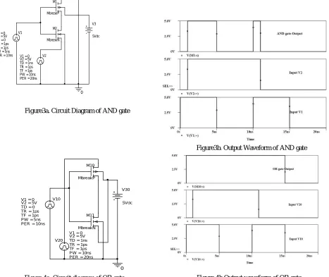
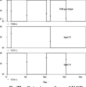
In conventional AND gates 3 CMOS gates are required, but now it uses only 1 CMOS. Thus the number of transistors is reduced as we expected. The simulation of 2 input substrate biased AND gate and its output waveform is shown in Fig. 3a and Fig. 3b respectively. Similarly to design a OR gate, in3 is made as high, which reduces the equation (1) as
Out = (in1.(in2)’)+(in2.1) (5) Out = in1+ in2 (6)
To design a XOR gate, in3 is made as equal to inversion of in1, which reduces the equation (1) as Out = (in1.(in2)’)+(in2.(in1)’) (7)
Out = in1 in2 (8)
In1
drain
drain
gate
gate
Source
Source
In2
Out
pMOS
nMOS
In3
0
V3
5Vdc V1
TD = 0
TF = 1ps PW = 5ns PER = 10ns V1 = 0
TR = 1ps V2 = 5V
V2
TD = 1ns
TF = 1ps PW = 10ns PER = 20ns V1 = 0
TR = 1ps V2 = 5V
M1
MbreakP
M2
MbreakN
Figure3a. Circuit Diagram of AND gate
Figure3b. Output Waveform of AND gate
V10
TD = 0
TF = 1ps PW = 5ns PER = 10ns V1 = 0
TR = 1ps V2 = 5V
M10
MbreakP
V20 TD = 1ns
TF = 1ps PW = 10ns PER = 20ns V1 = 0
TR = 1ps V2 = 5V
V30
5Vdc
M11
MbreakN
0
Figure 4a. Circuit diagram of OR gate Figure 4b Output waveform of OR gate
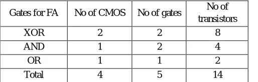
The simulation of 2 input substrate biased XOR gate and its output waveform is shown in Fig. 5a and 5b
V5 TD = 1ns
TF = 1ps PW = 10ns PER = 20ns V1 = 0
TR = 1ps V2 = 5V
M3 MbreakN M6 MbreakP V6 5Vdc 0 V4
TD = 0
TF = 1ps PW = 5ns PER = 10ns V1 = 0
TR = 1ps V2 = 5V
M4 MbreakN
M5
[image:4.612.81.548.86.479.2]MbreakP
[image:4.612.205.407.516.670.2]Figure 5b. The Output waveform of XOR gate
B. Design Of Full Adder
A combinational circuit consists of logic gates whose outputs at any time are determined directly from the present combination of input without regard to previous inputs. Arithmetic circuits fall under the category of combinational circuit. Adders form an basic component in applications like DSP architectures , microprocessor etc. The binary adders are used to add two binary numbers. Apart from basic addition the arithmetic operations that can be computed in electronic component are Shift/extension operation, equality and Magnitude comparison, increment/decrement, Complement, Sum, Multiplication, division, square root, trigonometric functions [3]. Hence we started out work with the basic adders. The full adder accepts three inputs – two input bits and the input carry, and generate sum output and carry output. The logic equations can be given as
Sum = A B C (9)
Carry = (A.B) + (B.C) + (C.A) (10) The logic diagram for the full adder is shown below in Figure 6.
A
1
2
3
Sum
Carry
U1A 1
2 3
C
1
2
3
1
2 3
1
2
3
[image:5.612.231.380.75.227.2]B
Figure 6. The Circuit diagram of Full adder
The Table 1 shows the truth table of a full adder which includes all the possible combinations of inputs.
Table1. Truth table of a Full Adder Inputs Outputs
A B C Sum Carry
0 0 0 0 0
0 0 1 1 0
0 1 0 1 0
0 1 1 0 1
1 0 0 1 0
1 0 1 0 1
1 1 0 0 1
1 1 1 1 1
gate. So to implement a full adder a sum of 10 CMOS devices are needed as summarized in Table2
Table 2 Details of CMOS required for Full Adder Gates for FA No of CMOS No of gates No of
transistors
XOR 4 2 16
AND 3 2 12
OR 3 1 6
Total 10 5 34
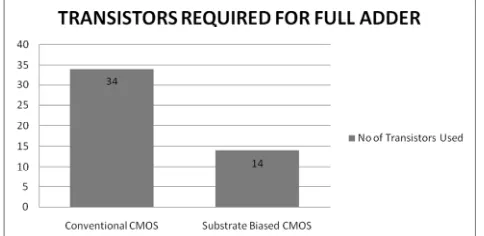
[image:6.612.182.439.262.344.2]But if substrate biased gates are used then it requires only 5 CMOS devices as summarized in Table3.
Table 3 Details of CMOS required for Substrate biased Full Adder
Gates for FA No of CMOS No of gates No of transistors
XOR 2 2 8
AND 1 2 4
OR 1 1 2
Total 4 5 14
Hence the substrate biased full adder is simulated with PSPICE schematic Entry. The number of transistors used is 14 instead of 34 as in the case of conventional CMOS Full adder.
0 M114 MbreakN M104MbreakP 0 V101 5Vdc M112 MbreakN VB
TD = 5ns TF = 1ps PW = 10ns PER = 20ns V1 = 0
TR = 1ps V2 = 5V
V100 5Vdc
M103
MbreakN
M108Mbreak P
M109Mbreak N
V104
5Vdc
0
M101MbreakN
VC TD = 0ns TF = 1ps PW = 20ns PER = 40ns V1 = 0
TR = 1ps V2 = 5V
V102 5Vdc 0 M113 MbreakP M110 MbreakN V105 5Vdc M107 MbreakP M105 MbreakP 0 M102 MbreakP VA
TD = 0 TF = 1ps PW = 5ns PER = 10ns V1 = 0
TR = 1ps V2 = 5V
M106 MbreakN V103 5Vdc M111 MbreakP
Figure7. Substrate biased Full adder circuit
Figure 8. Comparison of Substrate biased and Conventional CMOS devices
IV.CONCLUSIONS
From the results it can be observed that the number of transistors required to implement a Full adder is reduced considerably from 34 to 14. Thus we get the expected output. If this technique is implemented for other architectures the transistor count will be reduced. Even this full adder architecture can be enhanced by using multiplexer instead of gates which will further reduce the transistor count through which the power consumption is reduced.
REFERENCES
[1] Saroj Kumar, “Digital Circuit Design Using CMOS Transistor Model for Development in ASIC/SOC Technology,” Phil. Trans. Roy. Soc. London, vol. A247, pp. 529–551, April 1955.
[2] K. Navi, O. Kaehi, M. Rouholamini, A. Sahafi, S.Mehrabi, N. Dadkhahi, ―Low power and High performance 1-bit CMOS fill adder for nanometer design‖.
IEEE computer Society Annual Symposium VLSI (ISVLSI),
[3] John P. Uyemura, (2002) Introduction to VLSI Circuits and Systems, John Wiley & Sons.